中 文 摘 要 : 本研究使用的是利用高真空濺鍍法生成Ge薄膜搭配熱擴散製程結合 Si與Ge,生成SiGe合金,並透過化學蝕刻法製程去除殘存的Ge,成 功的製作出多晶Si/SiGe核殼無接面聚集型場效電晶體。其中Si內核 的高度為30奈米,SiGe殼層薄膜的厚度約為2nm。 在元件製作完成後,我們從不同的通道寬度與閘極長度切入,廣泛 地討論了單晶Si/SiGe殼層無接面聚集型場效電晶體的電性。本研究 製作SiGe薄膜的熱擴散製程條件有三種,並分別生成三種不同比例 的SiGe。其中,當退火條件為700度6小時的電性表現相較其他兩種 條件較不理想,我們推測是Ge因為過高的熱預算重新析出而無法生 成SiGe薄膜導致。我們選擇了無接面聚集型(junctionless accumulation mode)電晶體希望可以避免短通道效應,但在電性結 果的表現上,仍然可以從VTH的偏移現象與嚴重的DIBL表現觀察到短 通道效應。儘管如此,此新製程製作出的元件驅動電流與傳統平面 場效電晶體相比仍有很好的表現。 中 文 關 鍵 詞 : 矽鍺, 殼核結構,無接面聚集型電晶體
英 文 摘 要 : this study is through high vacuum sputter to producing Ge thin film and combine Si and Ge to match the SiGe alloy by thermal diffusion process. Furthermore, though chemical etching process to remove residual Ge achieve to product poly Si/SiGe core-shell Juctionless accumulation mode (JAM) FinFET. The height of Si core is 30 nm and the thickness of Si/SiGe core-shell is about 2 nm.
After finishing the fabrication of devices, we widely study the electrical characteristics of single Si/SiGe core-shell JAM FinFET transistors from a view of different Lg and Wch. The thermal diffusion process condition for this study are three and for fabricating three different content of Ge for each. We surmise that, among them, the annealing condition at 700C for 6 hours shows undesired electrical
characteristics against the others result from over thermal budget cause a plenty of Ge to precipitate against to form SiGe thin film. We choose JAM transistors to hope to
prevent short channel effect (SCE) but from the result of electric characteristics is still observed SCE with VTH offset phenomenon and severe Drain Induced Barrier Lowering (DIBL). Despite it, through this new process can still fabricate a comparable performance to classical planar FinFET in driving current.
I. Experiments
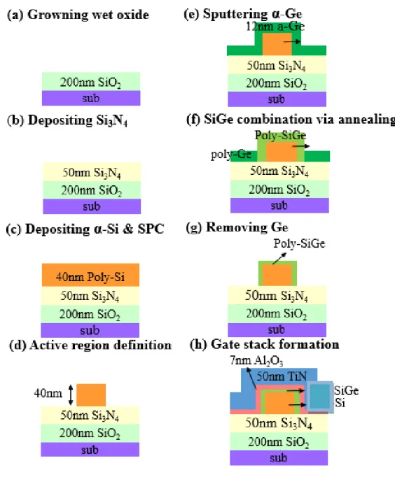
Main process flow is shown in fig.1-1. Device fabrication begin on a 6-inch Si
wafer grown with 200 nm wet oxide, after that, a 50-nm-thick Si3N4 layer is deposited
on it. Then the 40-nm-thick undoped amorphous Si (α-Si) layer is deposited via
low-pressure chemical vapor deposition (LPCVD) then α-Si is transform to poly-Si
through solid-phase crystallization (SPC) for 24 hrs at 600oC in N2 ambient.
The active region is defined by E-beam stepper and reactive-ion etching (RIE)
to form a single-Si fin-channel. Then the 12-nm-thick amorphous Ge (α-Ge) layer is
deposited by sputter and 20-nm-thick PESiO2 is deposited on amorphous Ge layer to
prevent Ge from oxidation in the thermal process. The combination of amorphous Ge
between single-Si is via the horizontal furnace tube in different annealing temperature
and time to form the different Ge content in SiGe channel. However, the Ge
completely covers whole wafer during sputtering. Because the etching selective ratio
between SiGe and Ge is different, we depend wet etching method to remove the
residual Ge on the Si3N4 layer. We choose the etching solution from a few papers and
choose the best choice is (HCl+H2O2) : H2O 0.5% at the room temperature. After
forward mention process, the single-Si core/single-SiGe shell structure channel.is
perfectly be fabricated. Next, the gate oxide in 7-nm-thick Al2O3 deposited by ALD
and the TiN is deposited immediately as gate metal. After the gate patterning, B11+
implantation (1 × 1015 cm-2 at 10 keV) was carried out to form p-type S/D and the
II. Results and discussions
2.1 Transmission Electron Microscopy
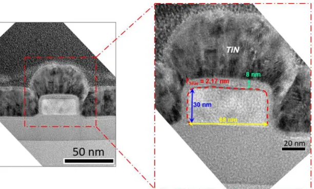
Figure 2-1 shows the cross-sectional transmission electron microscope (TEM)
image of single-Si/SiGe core-shell JAMFET. In fig. 2-1, a rectangular shape
core-shell structure is successfully fabricated with channel width (Wch) × channel
height (Hch) of 68 nm × 30 nm, and effective width (Weff) is 128 nm. We observe that
the white region is a 2.17 nm-thick thin SiGe layer cladding a 30 nm-thick single Si
layer after chemical solution etching. And a 5.16 nm-thick Al2O3 layer and a 63.25
nm-thick TiN surround the core-shell channel.
Figure 2-1 Cross-sectional TEM image of single-Si / SiGe core-shell
JAMFETs along the gate (b) The enlarged TEM image with H
ch= 30
nm, W
ch= 68 nm
2-2 X-ray photoelectron spectroscopy
We expect that the specific condition of annealing can combine Ge and Si at the
channel surface but rarely penetrate Ge into Si. There are three various SiGe
combination annealing condition that 1hr at 600oC、1hr at 700oC and 6hrs at 700oC in
SiO2 / substrate.
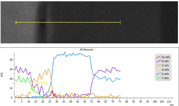
Figure 2-2 shows the depth profile of active region after the SiGe combination
annealing by the X-ray photoelectron spectroscopy. As shown in fig. 3-2, the SiGe
shell composition can be observed, the content of Ge at the channel surface are
20.8%、36.4% and 32.9% for different annealing condition that 1hr at 600oC、1hr at
700oC and 6hrs at 700oC respectively. In addition, no matter which annealing
condition is, the profile of Ge has higher content at the surface forming a SiGe alloy.
When etching depth reaches a deeper position, the Ge content decrease obviously
about below 5%.
It is noteworthy that when the combination annealing temperature is 700oC
more Ge penetrating into the Si layer than annealing temperature is 600oC. Hence, the
higher annealing temperature is, the severer Ge penetration is.
0
100
200
300
400
500
600
0
20
40
60
80
100
Atomic (%)
Etch time (s)
Si O Ge @ 600oC_1H Ge @ 700oC_1H Ge @ 700oC_6H2-3 Energy Dispersive Spectrometer
Finally, SiGe is detected on the shell of this structure through energy dispersive
spectrometer (EDS). In fig. 3-3 we can demonstrate that the element content on the
shell of silicon and germanium is 85.35% and 14.65%.
Figure 2-3 The element content distribution of single-Si / SiGe
core-shell JAMFETs by energy dispersive spectrometer
Element (nt) Atomic (%)
Si
Ge
III. Summary
In conclusions, we have demonstrated a single-Si /SiGe core-shell structure and
investigated the electrical characteristics of single-Si /SiGe core-shell JAMFETs.
The experimental results can be confirmed in the cross-sectional transmission
electron microscope (TEM) image and energy dispersive spectrometer (EDS). A
single-Si /SiGe core-shell gate stack is displayed in cross-sectional transmission
electron microscope (TEM) image. There is a very thin SiGe layer cladding the Si fin
forming a Si/SiGe core-shell structure.
In studying in the terms of the electrical performance of Ion and S.S., we can
imagine that SiGe combination in the condition of 1hr 600oC precisely transfer and
effectively enhance the electrical characteristics. Compare to above results, the Ion of
SiGe combination in the condition of 6hrs 700oC doesn’t show the behavior which SiGe can strengthen the drive current. Also, the value of DIBL of SiGe combination
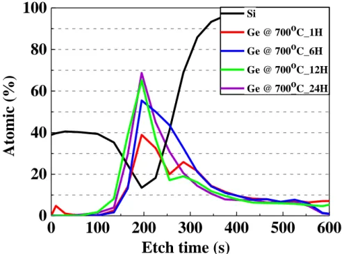
in the condition of 6hrs 700oC is two times higher than previous conditions. From fig.
2-19 we can recognize that Ge is precipitated due to over thermal budget treatment in
0
100
200
300
400
500
600
0
20
40
60
80
100
Atomic (%)
Etch time (s)
Si Ge @ 700oC_1H Ge @ 700oC_6H Ge @ 700oC_12H Ge @ 700oC_24H中英文摘要及關鍵詞 隨著半導體元件尺寸微縮之需求,矽基電晶體已達到其材料限制,故研究新 型可替代矽的新材料越顯重要。本報告中,將研究半導體高移動率新型材料─矽 鍺化合物半導體,以超高真空化學氣相沉積(UHVCVD)磊晶矽鍺薄膜後,使用離 子佈值(Ion Implant)技術並探討 P 型載子硼之活化情形,磊晶矽鍺薄膜中應力效 應可提升矽鍺化合物之移動率,進一步成為取代半導體矽通道材料之優勢,為了 維持磊晶矽鍺薄膜之應力且同時達到載子活化效果,本報告利用了新型退火方式 ─低熱預算之微波退火探討新材料的活化及應力維持之研究。 本報告中,將分成兩部份:不同載子離子佈值進不同鍺比例之磊晶矽鍺薄膜 與非晶化高溫離子佈值之研究。第一部分,以不同載子之離子佈值(硼,矽與硼) 摻雜進入不同鍺比例之矽鍺材料,接著使用低能量微波退火製程與傳統 RTA,並 以阻值、磊晶薄膜繞射分析、TEM、拉曼光譜、霍爾量測等分析方法做比較,發 現使用一階段微波退火能量 3P,能使硼離子佈值進 30% Ge 比例之矽鍺材料有 最低的阻值(170 ohm/sq)、最佳的磊晶薄膜品質、最小的佈值缺陷厚度(16nm)及 最好的殘留應力指數(1.48%),第二部分,發現非晶化離子佈值(矽與硼)且使用 150 度高溫離子佈值製程可有效降低非晶化離子佈值對於矽鍺材料所造成之晶格破 壞,且在微波退火能量 3.5P 時能使 40% Ge 比例之矽鍺材料有最佳的阻值與缺 陷厚度之表現,接著使用兩階段微波退火能量 3P+1P 持續時間 100 秒,能在不 發生應力鬆弛的情況下有效地提高摻雜硼離子活化程度(activation level),其片電 阻值低至 134.6 ohm/sq,霍爾量測之遷移率 302.7 cm2/Vs。
As the miniaturization of the size of semiconductor components, the silicon-based transistor has reached its material limitations, so that researching the new materials (silicon-germanium compound) to replace silicon is more important. The ion implantation technology is conducted to discuss the activation issue of p-type dopants, due to silicon-germanium epitaxial layer has the stress effect to enhance the carrier mobility, it is in a conflict of high-temperature annealing. In order to maintain the stress of the epitaxial silicon germanium layer and achieve the activation level of the carrier at the same time, this paper explores a new annealing method - microwave annealing (MWA) with the low thermal budget.
In this study, we have investigated that using one-step microwave annealing energy in 3P (1P = 600W), which can make boron implanted into 30% Ge content of silicon germanium layer has the lowest sheet resistance (170 ohm / sq), the best epitaxial layer quality and the better residual stress index (1.48%). However, using two-step microwave annealing energy in 3P+1P over 100s, it can further achieve higher activation level for Si0.7Ge0.3: B sample without stress relaxation. (Sheet resistance as
low as 134.6 ohm / sq, Hall measurement mobility of 302.7 cm2 / Vs.).
報告內容
1. Introduction
In scaling down the physical gate length of metal-oxide-semiconductor field effect transistors (MOSFETs) to 10/7 nm by 2017 to meet the roadmap of IMEC in 2015 [1], therefore, several challenges must be overcome. One of the main challenges is fabricating a front-end process for high-performance devices that is accurate control of the placement of the active doping regions. To keep the junction and contact resistance low, high temperature anneals have been extensively studied to electrically activate implanted dopants and repair lattice damage created after ion implantation to reduce junction leakage currents. Although these high temperature-annealing methods have demonstrated some successful applications to the source/drain anneal, they all still have a number of problems that make processing more complicated. Because the source/drain extension in the devices simultaneously requires shrinking junction depths and improved abruptness to increase device performance with high transistor drive current.
According to IMEC logic roadmap, Silicon-Germanium compound has been chosen to be the new promising materials and could replace silicon as channel materials in the future. Like Ge and III–V compound, SiGe has higher hole mobility due to its stress effect. Because of the different lattice constant between Si and Ge, SiGe will induce the stress on channel area to gain higher mobility.
The main challenge about SiGe is strain conservation, the interface layer will cause misfit dislocation and induce stress relaxation during the thermal process, as shown in Figure 1. The stress is the critical factor about the high mobility semiconductor channel material. The greatest challenge is to achieve very steep and highly doped regions of strained layers while conserving their elastic strain at the same time since strain is responsible for carrier mobility enhancement [2].
Fig. 1 Misfit dislocation on SiGe interface layer.
wavelength of 248nm to study doping activation of biaxially compressively strained Si1-xGex/Si heterostructures. High temperature rapid thermal annealing (RTA) is
employed, but this is in conflict with the low thermal budget, required to avoid strain relaxation and Ge inter-diffusion in SiGe heterostructures.
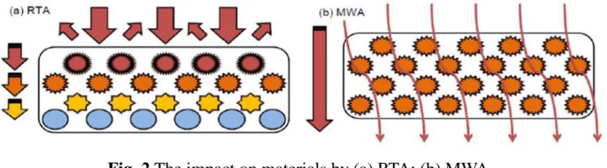
MWA is a potential solution for implanted Silicon or Germanium annealing on our previous work [6-11] because it takes place at a low temperature that restrains diffusion and results in good activation. The impact of annealing is only on the surface for conventional annealing methods. It needs the more high temperature to impact deeper position of materials, and the high temperature with the large thermal budget will lead to diffusion. However, the impact of microwave annealing on the material is able to be inside-out and get more uniform annealing effects as shown in Figure 2.
Fig. 2 The impact on materials by (a) RTA; (b) MWA.
In this paper, high current and low energy ion implantation and low-temperature microwave annealing were employed to achieve ultra-shallow junction and conserve the elastics train in the SiGe layer. In order to use the characteristic of microwave annealing more effectively, two-step microwave annealing was also employed. In the first step, a high power 1800W~2400W microwave was used to achieve solid phase epitaxial regrowth (SPER) and enhance microwave absorption. In the second step, unlike traditional thermal annealing which requires higher energy to activate the dopant, a 300W~600W microwave was used to achieve low sheet resistance.
2. Experimental Procedures
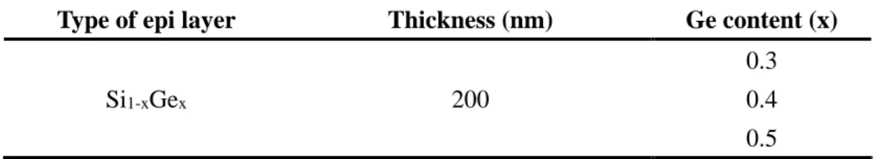
of Si and SiGe epitaxial films at the growth temperature. The structure and splittable are shown in Figure 3 and Table 1, respectively. Then all wafers were implanted with boron ion (10keV @5E15 atoms/cm2) at wafer chuck temperature 150°C and 7o tilt angle to avoid channeling effects. Annealing of the samples by using different tools like microwave annealing and rapid thermal annealing. Microwave magnetron power ranged between 1P (1P = 600W, about 250°C) and 5P (550°C) for 100 seconds, using an AXOM-300, which is a multimode chamber manufactured by DSG Technologies. Wafer temperatures during MWA were monitored by a pyrometer with a direct line of sight to the lower surface of a three-wafer stack in the chamber. The frequency of the microwave was 5.8 GHz. The MWA process time was defined as the duration for which the microwave magnetron was turned on. The temperature range of RTA was set at 450 °C~850 °C for 10 seconds. To investigate the characteristics of dopant activation, a four-point probe was used to measure the sheet resistance Rs. To investigate the lattice recovery and recrystallize, Raman spectrum was measured and compared. To investigate the characteristics of dopant deactivation, Hall measurement was carried out to determine resistivity, carrier concentration, and carrier mobility. Before Hall measurement, sputtering was used to deposit electrical poles on the samples for Hall measurement.
Fig. 3 Structure of the experiment sample. Table 1 Split table of Ge content.
Type of epi layer Thickness (nm) Ge content (x)
Si1-xGex 200
0.3 0.4 0.5
3. Results and discussion
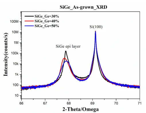
Therefore, higher Ge content of SiGe, the worst quality of the epitaxy layer.
Fig. 4 XRD measurement of SiGe as-grown samples with different Ge content.
Fig. 5 Raman spectrum of SiGe as-grown samples with different Ge content.
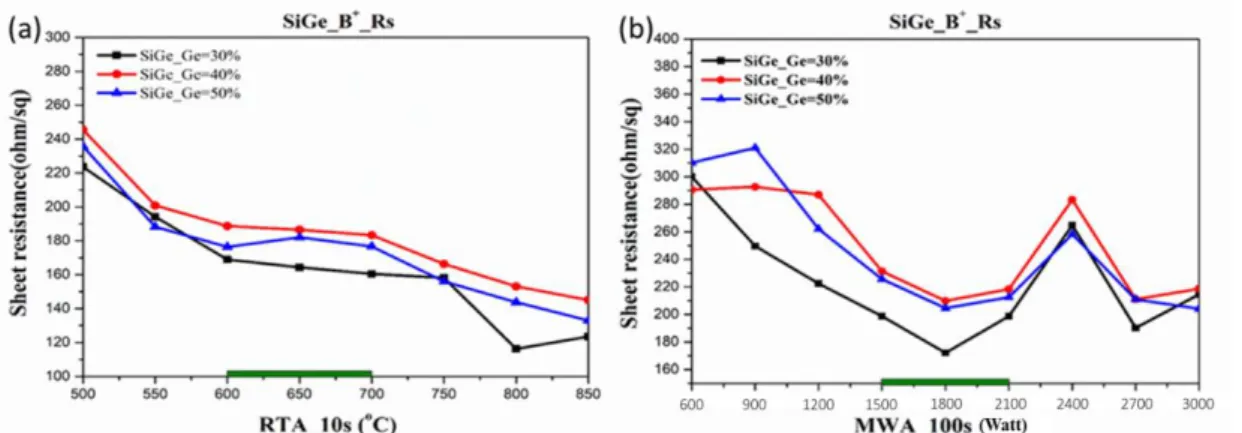
Figure 6 shows the sheet resistance of Si1-xGex: B at x in 0.3~0.5 samples after
RTA annealing at 500℃~850℃ for 10s and MWA annealing at 1P~5P for 100s, respectively. The minimum sheet resistance occurs around 170 ohm/sq by RTA at 600℃ and by MWA at 3P. RTA is the thermal process by heat transfer from the top to internal of the sample, so the deeper dopants may not absorb the equal thermal energy compare to the top of dopants. Due to the heat transfer efficiency is different by depth, the electrical characterization is not distinguishable from 600℃ to 700℃. However, all the samples annealed by MWA minimize the sheet resistance on 3P region but degraded on higher power which independent on Ge content. It can indicate that SiGe materials are very sensitive to temperature by an annealing process.
Fig. 6 The sheet resistance of the boron implanted samples annealed by (a) RTA, (b)
MWA with different Ge content.
the epitaxy layer quality. A shoulder appears at the left of the (004) peak after B+ implantation. That would mean that a more compressively strained thin layer is formed due to implantation. Pendellosung fringes may be superimposed on the shoulder, but they should be observed symmetrically around the main peak. There is perhaps too noise between the (004) reflections of substrate and layer for seeing them. It is interesting to observe that the shoulder disappears after RTA at 800℃ or MWA at 4P. That suggests that a thin layer enriched in Ge has been formed at the SiGe/Si interface by incorporation of recoil Ge atoms in substitutional sites. Annealing induces the diffusion of Ge atoms and/or relaxation of the whole layer and consequently, the Ge-rich interface layer would vanish. Figure 7 can observe that annealed by RTA at 600℃ and by MWA at 3P show more visible fringes than other temperature (power), it corresponds to the electrical characterization result for the annealing energy that makes the lowest sheet resistance.
Fig. 7 XRD curve of Si0.7Ge0.3: B annealed by (a)RTA, (b)MWA in different
temperature and power, respectively.
The end-of-range defect thickness measure by TEM as shown in Figure 8. For Si0.7Ge0.3: B samples whose amorphous layer thickness is around 46nm, then annealed
Fig. 8 TEM images of Si0.7Ge0.3: B samples w/o annealing by (a) RTA 600℃ to 800℃
for 10s and (b) MWA 2.5P to 3.5P for 100s.
To activate dopants effectively needs a higher temperature, but the higher temperature may be easy to cause stress relaxation in SiGe lattice. Figure 9 shows the Raman spectrum of Si0.7Ge0.3: B sample annealed by RTA and MWA. Base on the
position of the Si-Si vibration modes, the elastic strain in the SiGe layer can be calculated according to equation (1):
ɷSiGe=520.5-62*CSiGe-815*εSiGe (Eq.1) [2]
where ɷSiGe is the position of the Si-Si vibration mode within the SiGe layer, CGe
represents the Ge content, and εSiGe is the residual strain [12]. The large Raman shift
from Si-Si bonding around 510 cm-1 to 515 cm-1 indicate that the lower residual stress index, for Si0.7Ge0.3: B sample, which annealed by RTA in 800℃ and MWA in 3.5P to
4P. Both results show the maximum Raman shift value and have higher stress relaxation degree, it is an echo with epitaxy layer quality and TEM image.
different temperature and power, respectively.
Figure 10 shows the Hall effect measurement on Si0.7Ge0.3: B samples annealed by
RTA and MWA. The mobility in RTA and MWA are around 173 cm2 V-1s-1 at 600℃ and 270 cm2V-1s-1 at 3P, respectively. For higher RTA temperature samples, the mobility decreases severely, which caused by stress relaxation for high annealing temperature process. However, annealing by MWA is not the same track of RTA, it has the highest mobility, the lowest sheet resistance, better epitaxy layer quality and minimum end-of-range defect thickness at 3P. It can confirm that SiGe materials are very sensitive to annealing energy, the mobility will decrease as long as stress relaxation occurs. Our purpose is to highly activate dopants and avoid stress relaxation. Comparison of annealed by MWA at 3P and RTA at 600℃, those are the lower sheet resistance and better epitaxy layer samples, but the sample after MWA process has the higher mobility thus represents the higher activation level.
Fig. 10 The Hall Effect on Si0.7Ge0.3: B samples annealed by (a) RTA and (b) MWA in
different temperature and power, respectively.
In a previous study [7-8], two-step MWA process can effectively improve dopants activation level with second step low power MWA. Therefore, to further investigate, the low power MWA at 1P is after then high power at 3P to enhance the higher activation level without stress relaxation. In figure 11 shows the sheet resistance of Si0.7Ge0.3: B
samples annealed by two-step MWA in different annealing time. Obviously, two-step MWA (3P+1P) process can reduce the sheet resistance from around 170 ohm/sq to 135 ohm/sq, then changing the second-step annealing time didn’t influence the sheet resistance, it is assumed that the MWA energy is the main factor to lower the sheet resistance instead of MWA process time. Table 2 shows the Hall Effect measurement of Si0.7Ge0.3: B sample after two-step MWA, from first-step to second-step MWA,
was used to investigate. Based on electron relaxation process in the conduction band of the PL process, the stronger PL signals represent the better lattice arrangement and less damage in the internal SiGe lattice. In other words, if the annealing conditions have better lattice recovery and recrystallize status, the sample would have more obvious PL spectrum peak, as shown in figure 12. The two-step MWA (3P+1P) has the apparent peak compare to those one-step MWA (3P) and RTA (600℃), which corresponds to the result of two-step MWA can effectively improve SiGe lattice arrangement and make higher activation level for lower sheet resistance. For Si and Ge bulk materials, the apparent peak signal is around 1100 and 1500 nm, respectively. So SiGe materials have a reasonable apparent peak around 1300 nm, which PL apparent signals can calculate the material bandgap.
Fig. 11 The sheet resistance of Si0.7Ge0.3: B samples annealed by two-step MWA in
different annealing time.
Table 2 The Hall Effect of Si0.7Ge0.3: B samples annealed by two-step MWA in different
annealing time.
Remark Annealing Resistivity
Fig. 12 PL spectrum of Si0.7Ge0.3: B samples and annealed by the different condition of
annealing.
Figure 13 shows the Raman spectrum to confirm the stress relaxation after two-step MWA process. To observe the position of the Si-Si vibration modes, the elastic strain in the SiGe layer can be calculated, compare to one-step MWA (3P), two-step MWA (3P+1P) process does not have obviously Raman shift. It investigated that the second step low power MWA energy can effectively lower sheet resistance for higher activation level but also without stress relaxation. The residual strain after different annealing conditions and correspond to sheet resistance are a list in Table 3. It is confirmed that one-step MWA has the ability to avoid stress relaxation compare to RTA based on almost same activation level (Rs), and two-step MWA process is able to get higher activation level (lower Rs) but without stress relaxation at the meantime.
Table 3 The residual strain results of Si0.7Ge0.3: B samples and annealed by the different
Fig. 13 Raman spectrum of Si0.7Ge0.3: B samples and annealed in different annealing
time.
4. Conclusion
參考文獻
[1] D. Vogler, “The Roadmap to 5nm: Convergence of Many Solutions Needed”, SEMICON West, 2015.
[2] G. Luong et al., “Study of dopant activation in biaxially compressively strained SiGe layers using excimer laser annealing”, Journal of Applied Physics, vol. 113, pp. 204902, 2013.
[3] R. Minamisawa et al., “p-type ion implantation in tensile Si/compressive Si0.5Ge0.5/tensile strained Si heterostructures”, Journal of The Electrochemical
Society, vol. 159, pp. H44-H51, 2011.
[4] B. Holländer et al., “Strain relaxation of pseudomorphic Si1− xGex ⁄ Si (100)
heterostructures after Si+ ion implantation”, Journal of applied physics, vol. 96, pp. 1745-1747, 2004.
[5] D. Buca et al., “Si+ ion implantation for strain relaxation of pseudomorphic Si1− xGex ⁄ Si (100) heterostructures”, Journal of applied physics, vol. 105, pp. 114905,
2009.
[6] S.G. Sundaresan et al., “Comparison of solid-state microwave annealing with conventional furnace annealing of ion-implanted SiC”, Journal of electronic materials, vol. 36, pp. 324-331, 2007.
[7] T-L Shih and W-H Lee, “High Dopant Activation and Diffusion Suppression of Phosphorus in Ge Crystal with High-Temperature Implantation by Two-Step Microwave Annealing”, ECS Transactions, vol. 72, pp.219-225, 2016.
[8] T-L Shih, Y-H Su, and W-H Lee, “High dopant activation of phosphorus in Ge crystal with high-temperature implantation and two-step microwave annealing”, Appl. Phys. Lett., vol. 109, pp.122103, 2016.
[9] W-H Lee, M-H Tsai and W-H Liao, “Studies on ultra-shallow junction 20nm P-MOS with 250°C microwave annealing for activation of boron dopants in silicon”, IIT Conference 2014.
[10] T-L Shih and W-H Lee, “Studies on Activation of High-Mobility III-V Group Semiconductor Materials by Using Microwave Annealing”, International Journal of Materials Science and Applications, vol. 6, pp.148-153, 2017.
[11] Y-J Lee et al., “Dopant activation in single-crystalline germanium by low-temperature microwave annealing”, IEEE Electron Device Letters, vol. 32, pp. 194-196, 2011.
出席國際學術會議心得報告
計畫編號 A1081-0811 計畫名稱 108-2622-8-006-009-TM 出國人員姓名 服務機關及職稱 張書維/國立成功大學/兼任助理 會議時間地點 美國舊金山 12/7~12/11會議名稱 國際電子元件會議(International Electron Devices Meeting)
發表論文題目 First demonstration of CMOS inverter and 6T-SRAM based on GAA CFETs structure for 3D-IC applications.
一、 參加會議經過
12/7 下午報到並參加會議所舉辦之 tutorial,該場主題為” Oxide Semiconductors and Application”
12/8 早上及下午皆參加會議所舉辦之 short course,該場主題為” Technology
Scaling in the EUV Era and Beyond”
12/9 早上參與開場演講,下午聽主題為”Monolithic 3D Integration and BEOL Transistors”之會議廳,晚上參加晚宴
12/10 早上聽主題為”Gate-All-Around Device Technologies”之會議廳並於該場進行 口頭報告,下午聽主題為”Emerging Devices for Extending Moore’s Law”之會 議廳
12/11 早上聽主題為” High Mobility Ge-Based Channel Devices”之會議廳,下午聽主 題為” CMOS Platform Technologies”之會議廳
人數、時間以及問題深度也都讓人感覺,大家對於彼此的研究都頗有興趣。到了口頭報告會 議時間,聆聽業界所提供的研究報告及結果,不僅能審視自己的實驗完整性及邏輯, 也能學到業界一些新的檢測及驗證實驗的方法,也都是平時在學校或其他會議較難 接觸到的,雖然通常業界團隊的分工較完整也較多資源,但仍可從其中斯可自己能 過做到的部分來加強自己的實力。而當輪到我上台報告時,緊張程度也是與以往非 常不同,下面聽眾 200~300 人且不乏有業界、學界資深且專業的人,在準備時就擔 心自己學識不足或是講得不夠精確遭到質疑,但最後順利結束,也得到許多聽眾的 讚賞以及引薦機會,不僅感受到此會議的高關注度,也增加自己被世界認識的機會。 三、 發表論文摘要
12/9 Open & Plenary Session
12/10 口頭報告以及會後聽眾討論
108年度專題研究計畫成果彙整表
計畫主持人:李文熙 計畫編號:108-2622-8-006-009-TM 計畫名稱:300mm變頻微波退火應用閘極全環鰭式場效電晶體之研發(1/2) 成果項目 量化 單位 質化 (說明:各成果項目請附佐證資料或細 項說明,如期刊名稱、年份、卷期、起 訖頁數、證號...等) 國 內 學術性論文 期刊論文 0 篇 研討會論文 1Study of plasma UV/VUV irradiation damage in Neutral beam Etching and Inductively coupled plasma Etching through analysis of Silicon MOS capacitor characteristics, 2019 IEDMS 專書 0 本 專書論文 0 章 技術報告 0 篇 其他 0 篇 國 外 學術性論文 期刊論文 1 篇
Advanced Low Damage Manufacturing Processes to Fabricate SOI