Chapter 3
An Optical Multiplexer for Pulse Train Generation
As mentioned in Chapter 1, the development of integrated optical
devices and all light wave circuit applied to communication transmission
has become the future trend. We propose optical splitter based sol gel glass
waveguide for optical time division multiplexer system in this chapter. This
chapter is organized as follows: Section 3-1 introduces the technique of
optical time division multiplexing. And we describe the theory of the
generation of pulse train based on optical time division multiplexer in
Section 3-2. In Section 3-3, we design optical light wave circuit system
based on MMI sol gel glass waveguide. The characteristics of our designed
system are also presented in Section 3-3. In the final Section 3-4, we give
the summary of our designed optical all light wave circuit time division
multiplexer systems.
3-1 Introduction of the optical time division multiplexing
Development of ultra high bit-rate telecommunication is requisite for demand for expanded transmission capacity. In order to satisfy these demands, high-speed and wide-band electronics in photonic transmitters and receivers for multi gigabit-per-second pulse-code modulated (PCM) systems is indispensable. The bit rate of electrical time-division-multiplexing (ETDM) system is currently limited to 100 Gbit/s. System speed is mainly limited by the speed of the electronic circuits we used. Although individual chips have been developed at higher data rate, these are only used in laboratory presently and methods of packaging have yet to be solved. One method to overcome this electronic speed bottleneck is to extend the well-known techniques of electrical multiplexing into the optical domain.
Optical time division multiplexing (OTDM) was first demonstrated as
early as 1968 [50], primarily as means to increase the capacity of an optical
link. And Optical multiplexing technology is developed in recently years,
and it offers some advantages, such as: enabling simple multiplexing,
demultiplexing and removing the need to electronically process all traffic
entering a node. The research of optical time division multiplexing and demultiplexing for very high bit-rate PCM systems has been demonstrated for more than three decades [51-54]. Technical progress has continued, with the world’s first 40 Gbit/s experiments carried out using OTDM [55].
Several techniques were reported to produce optical pulse trains with high quality. Although most of them operated at 10 GHz to achieve the 40 GHz repetition rate, source based on soliton are particularly attractive for their simplicity and stability. Soliton pulses can arise in the anomalous dispersion regime due to nonlinear fiber propagation, and it can be described by the nonlinear Schrodinger equation (NLSE). Soliton sources at 40 GHz were already demonstrated [56]. For OTDM applications, this source would need pulse compression since 160 Gbit/s requires pulsewidth values lower than around 2 ps. Indeed, pulse compression might be adopted by another soliton-based technique.
3-2 Theory of the generation of pulse train based on optical time division multiplexer
Extremely high bit-rate signal transmission can be achieved by optical
time-division multiplexing (OTDM). Demultiplexing of such signals has been reported using the Kerr effect in the optical fibers in a nonlinear optical loop mirror [57], [58] or four-wave mixing in nonlinear mediums, such as fibers [59], or semiconductor amplifiers [60]. Lasers generating ultra-short pulses at a high repetition rate or optical multiplexing of pulses with lower repetition rate are needed for ultra-high bit-rate optical signals.
All-optical pulse multiplexing can be achieved with bulk optics [61-62] or fibers [63]. Another way is to generate a high-repetition-rate pulse train by using one laser and a planar lightwave circuit (PLC). Such an experiment has been carried out by using X16 PLC multiplexer based on integrated silica single mode waveguides [64]. We report here the generation of a 40 GHz, 60 GHz, 80 GHz and 100 GHz optical pulse train by using a light wave circuit built on sol gel glass waveguide.
3-2-1 Basic principle of pulse train generation based on lightwave circuit
The basic principle of optical time-division multiplexing and
demultiplexing is that each of the baseband data streams is
allocated a series of time slots on the multiplexed channel. A multiplexer (MUX) assembles the higher bit-rate bit stream from several baseband streams and a demultiplexer (DEMUX) reconstructs bit streams at the original lower bit rate by separating bits in the multiplexed stream. The techniques for this process are well established for electrical time-division multiplexing and demultiplexing but are only now emerging in optical systems.
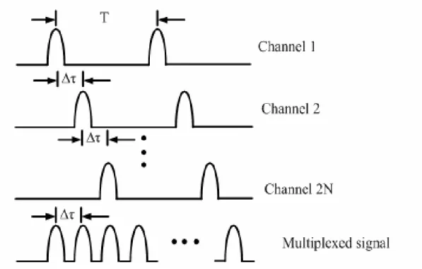
Fig.3-1. shows a schematic of 1x(2N+1) channel OTDM transmission system based on splitter we designed. A train of picosecond (ps) duration optical pulses from a suitable laser source is split 2N+1 ways by our designed power splitter. Each optical pulse train is individually modulated by an electrical data signal forming in N optical RZ format data channels.
Each branch is delayed by a fraction of the clock period and synchronized
to allow passive multiplexing to sum up an individual data stream. Here the
multiplexer we used is most simply implemented by using different length
fiber with appropriate optical delays between the channels. To avoid
crosstalk between these interleaved channels, the laser source must be able
to generate optical pulses of duration < 1/N of the clock period. We design
different length of fiber in each channel to delay the optical pulse trains. To
multiplex an optical signal with period T ps to channel 2N+1, the required time delay Δ τ
ifor each path is:
50( )
i
i T i ps
τ N
Δ = ⋅ = × , i =1,2,…, N-1 (3-1)
i i
L c
τ n
Δ = Δ , i =1,2,…, N-1 (3-2)
The timing scheme is shown on Fig.3-2. We can obtain the required difference of the fiber length Δ L
ito cause the corresponding time delay in each path. In (3-1) and (3-2), the symbol Δ L
iis the difference length for ith fiber. Δ τ
iis the time delay for ith path, c is the speed of light in the vacuum, n is the refractive index of fiber core. The difference of the difference of the fiber length Δ L
iand the time delay Δ τ
iis in terms of the first path. For example, for multiplexing the optical pulse train of 10Gbit/s to 40Gbit/s, the period T is 25 ps, so the time delay is 3.125 ps, and the difference of the fiber length is 0.2mm.
Optical amplifiers are used to maintain the correct signal power to keep
sufficient signal to noise ratio for acceptable bit-error rate. In such systems,
fiber dispersion can be managed in many ways. One method is to balance
the average group velocity dispersion in the whole system such that it is
zero referred to dispersion management and another is to use soliton
transmission techniques. Demultiplexing and clock recovery allows the input optical signal to be split into discrete channels.
3-3 Design and analysis of the generation of pulse train based on optical time division multiplexing
The demonstrated optical multiplexer generates, from a single pulse at the input, a train of 2N+1 pulses uniformly temporally spaced at the output.
The input light pulse is split into 2N+1 balanced parts by a multimode interference (MMI) splitter and each part is coupled to 2N+1 fiber of designed different lengths. The propagation time difference between two consecutive paths is Δτ ps. Then, a 2N by 1 combiner gathers these 2N+1 pulses toward a unique single mode output waveguide.
3-3-1 Generation of pulse train based on 1x3 MMI power splitter
With 18-μm-wide and 492.3-μm-length multimode waveguide of 1x3
power splitter, and connecting the designed fiber length are L, L+ΔL,
L+2ΔL, respectively. According (3-1) and (3-2), we can calculate that ΔL
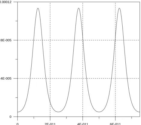
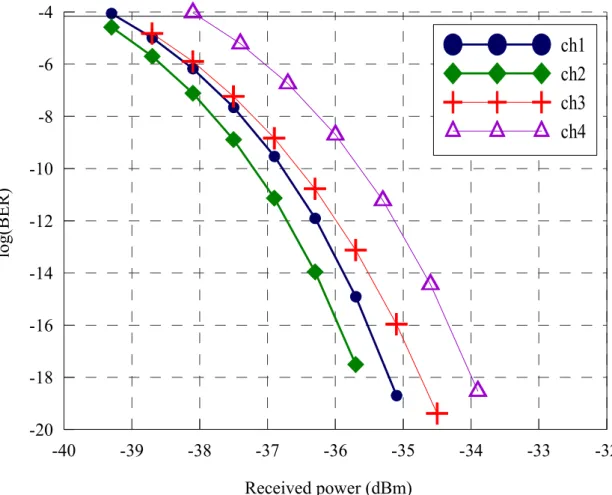
for the 40 GHz pulse train is 4557μm. And in other side, we use a 3x1 coupler to connect the different length fiber. After propagation in fiber, we notice that the light is perfectly split in three balanced parts. Fig.3-3 presents a BPM simulation of the 1x3 MMI power splitter. Following we input a continuous pulse train at repetition rate of 10 GHz to the optical time division multiplexer system as shown in Fig. 3-1. The signal is booted in an erbium doped amplifier (EDFA) before being split into three channels by a 1x3 power splitter. Each of the three 10 GHz repetition rate optical pulse trains is modulated individually. Before recombining the data streams by using a 3x1 power splitter, each path passes through a variable delay line interleave a single 40 Gbit/s RZ data stream with the correct delay. The receiver is consisted of an EDFA, an oscilloscopo. Fig. 3-4 shows the OTDM measurement trace. Fig. 3-5 shows the relation of bit-error rate and received power for each output ports. The receiver sensitivity for BER of 10
-9is -37dBm and -36.7dBm respectively for channel 1 and channel 2.
And one of three output ports is employed as a monitor.
3-3-2 Generation of pulse train based on 1x5 MMI power
splitter
With 30-μm-wide and 1203-μm-length multimode waveguide of 1x5 power splitter, and connecting the designed single mode waveguide length are L, L+ΔL, L+2ΔL, L+3ΔL, L+4ΔL respectively. According (3-1) and (4-2), we can calculate that ΔL for the 50 GHz pulse train is 3646μm. And in other side, we use a 5x1 coupler to connect the different length fiber.
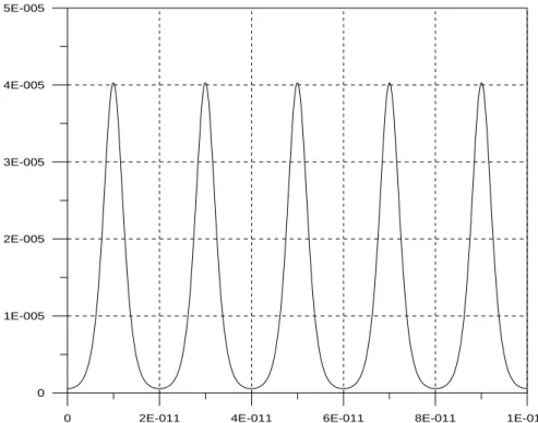
After propagation in fiber, we notice that the light is perfectly split in three balanced parts. Fig. 3-6 shows a BPM simulation of the 1x5 MMI power splitter. Following we input a continuous pulse train at repetition rate of 10 GHz to the optical time division multiplexer system as shown in Fig. 3-1.
The signal is booted in an erbium doped amplifier (EDFA) before being
split into three channels by a 1x5 power splitter. Each of the five 10 GHz
repetition rate optical pulse trains is modulated individually. Before
recombining the data streams by using a 5x1 power splitter, each path
passes through a variable delay line interleave a single 50 Gbit/s RZ data
stream with the correct delay. The receiver is consisted of an EDFA, an
oscilloscopo. Fig. 3-7 shows the OTDM measurement trace. Fig. 3-8 shows
the relation of bit-error rate and received power for each output ports. The
receiver sensitivity for BER of 10
-9is -37.1dBm, -37.5dBm, -36.8dBm, -36dBm respectively for channel 1, channel 2, channel 3, channel 4. And one of five output ports is employed as a monitor.
3-3-3 Generation of pulse train based on 1x7 MMI power splitter
With 42-μm-wide and 2763-μm-length multimode waveguide of 1x7 power splitter, and connecting the designed single mode waveguide length are L, L+ΔL, L+2ΔL, L+3ΔL, L+4ΔL, L+5ΔL, L+6ΔL respectively.
According (3-1) and (3-2), we can calculate that ΔL for the 80 GHz pulse
train is 2278μm. And we use a 7x1 coupler to connect the different length
fiber. After propagation in these single mode waveguides, we notice that
the light is perfectly split in three balanced parts. Fig. 3-9 shows a BPM
simulation of the 1x7 MMI power splitter. Following we input a continuous
pulse train at repetition rate of 10 GHz to the optical time division
multiplexer system as shown in Fig. 3-1. The signal is booted in an erbium
doped amplifier (EDFA) before being split into three channels by a 1x7
power splitter. Each of the three 10 GHz repetition rate optical pulse trains
is modulated individually. Before recombining the data streams by using a 7x1 power splitter, each path passes through a variable delay line interleave a single 80 Gbit/s RZ data stream with the correct delay. The receiver is consisted of an EDFA, an oscilloscopo. Fig. 3-10 shows the OTDM measurement trace. Fig. 3-11 shows the relation of bit-error rate and received power for each output ports. The receiver sensitivity for BER of 10
-9is -37dBm, -38dBm, -36.8dBm, -36.7dBm, -36.7dBm, -35.7dBm respectively for channel 1, channel 2, channel 3, channel 4, channel 5, channel 6. And one of seven output ports is employed as a monitor.
3-3-4 Generation of pulse train based on 1x9 MMI power splitter
With 54-μm-wide and 6000-μm-length multimode waveguide of 1x9
power splitter, and connecting the designed single mode waveguide length
are L, L+ΔL, L+2ΔL, L+3ΔL, L+4ΔL, L+5ΔL, L+6ΔL, L+7ΔL, L+8ΔL,
respectively. According (3-1) and (3-2), we can calculate that ΔL for the
100 GHz pulse train is 1823μm. And in other side, we use a 9x1 coupler to
connect the designed single mode waveguide. After propagation in these
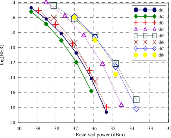
single mode waveguides, we notice that the light is perfectly split in three balanced parts. Fig. 3-12 presents a BPM simulation of the 1X9 MMI power splitter. Following we input a continuous pulse train at repetition rate of 10 GHz to the optical time division multiplexer system as shown in Fig. 3-1. The signal is booted in an erbium doped amplifier (EDFA) before being split into three channels by a 1x9 power splitter. Each of the three 10 GHz repetition rate optical pulse trains is modulated individually. Before recombining the data streams by using a 9x1 power splitter, each path passes through a variable delay line interleave a single 100 Gbit/s RZ data stream with the correct delay. The receiver is consisted of an EDFA, an oscilloscopo. Fig. 3-13 shows the OTDM measurement trace. Fig. 3-14 shows the relation of bit-error rate and received power for each output ports.
The receiver sensitivity for BER of 10
-9is -37.3dBm, -37.8dBm, -37.1dBm,
-36.3dBm, -35.7dBm, -37dBm, 35.7dBm, 35.9dBm respectively for
channel 1, channel 2, channel 3, channel 4, channel 5, channel 6, channel 7,
channel 8. And one of nine output ports is employed as a monitor.
3-4 Summary
Our designed optical multiplexer for pulse train generation based on
light wave circuit with 1x(2N+1) sol gel power splitter are successfully
demonstrated. This multiplexer is based on a MMI splitter, several fiber of
different length. And we successfully generate 40Gbit/s, 50Gbit/s, 80Gbit/s,
100Gbit/s optical pulse train by using an optical multiplexer based on
1x(2N+1) sol gel MMI splitters. In table 3-1, it shows that the value ofΔτ,
ΔL, we use and the generation of pulse frequency we get.
10 G H z pul se la ser 1x (2 N+1 ) splitter (2N+1)x1 co mb in er
AM AM AM AM
EDFA ED FA EA modul a to r Clock reco ver y
Pi n- PD low-pass fi lt er BER cou n ter
10 Gbit/s RZ, electri cal sig n a l monitor (a ) T ransmitter (b) Receiver
Figure. 3-1 (a) transmitter and (b) receiver of the OTDM systemFig. 3-3 BPM simulation of the 1x3 MMI splitter operation
Fig. 3-2 Timing scheme for multiplexing in an n-channel OTDM
0 2E-011 4E-011 6E-011 0
4E-005 8E-005 0.00012
Fig. 3-5 BER versus received power for applying 1x3 optical Fig. 3-4 Simulation of pulse train trace for using 1x3 power splitter
-39 -38.5 -38 -37.5 -37 -36.5 -36 -35.5 -35 -34.5 -34 -20
-16 -12 -8 -4
-18 -14 -10
-6 ch1
ch2
log(BER)
Received power (dBm)
0 2E-011 4E-011 6E-011 8E-011 1E-010 0
1E-005 2E-005 3E-005 4E-005 5E-005
Fig. 3-6 BPM simulation of the 1x5 MMI splitter operation
Fig. 3-7 Simulation of pulse train trace for using 1x5 power splitter
Fig. 3-8 BER versus received power for applying 1x5 optical splitter
Fig. 3-9 BPM simulation of the 1x7 MMI splitter operation
-40 -39 -38 -37 -36 -35 -34 -33 -32
-20 -16 -12 -8 -4
-18 -14 -10
-6
ch1
ch2 ch3 ch4
log(BER)
Received power (dBm)
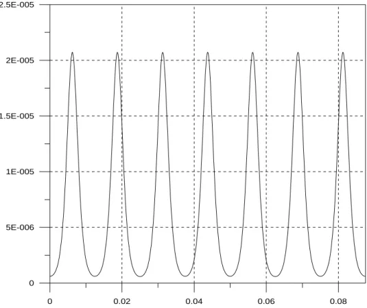
0 0.02 0.04 0.06 0.08 0
5E-006 1E-005 1.5E-005 2E-005 2.5E-005
Fig. 3-11 BER versus received power for applying 1x7 optical splitter
Fig. 3-10 Simulation of pulse train trace for using 1x7 power splitter
-42 -41 -40 -39 -38 -37 -36 -35 -34 -33 -32
-20 -16 -12 -8 -4
-18 -14 -10 -6
ch1 ch2 ch3 ch4 ch5 ch6
log(BER)
Received power
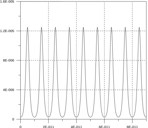
0 2E-011 4E-011 6E-011 8E-011 0
4E-006 8E-006 1.2E-005 1.6E-005
Fig. 3-12 BPM simulation of the 1x9 MMI splitter operation
Fig. 3-13 Simulation of pulse train trace for using 1x9 power
splitter
Splitter output ports
Δτ (ps) ΔL (μm) Input pulse frequency
(Gbit/s)
Output pulse frequency
(Gbit/s)
3 25 4557 10 40
5 20 3646 10 50
7 12.5 2278 10 80
9 10 1823 10 100
Table 3-1 The relation of splitters output posts for
Δτ, ΔL, and Output pulse frequency-40 -39 -38 -37 -36 -35 -34 -33 -32
-20 -16 -12 -8 -4
-18 -14 -10 -6
ch1 ch2 ch3 ch4 ch5 ch6 ch7 ch8
log(BER)
Received power (dBm)