Ultraviolet photodetectors based on selectively grown ZnO nanorod arrays
L. W. Ji,1,a兲S. M. Peng,2Y. K. Su,2S. J. Young,2C. Z. Wu,1and W. B. Cheng1 1Institute of Electro-Optical and Materials Science, National Formosa University, Yunlin 632, Taiwan 2Institute of Microelectronics and Department of Electrical Engineering, National Cheng Kung University, Tainan 701, Taiwan
共Received 20 January 2009; accepted 30 April 2009; published online 20 May 2009兲
Metal-semiconductor-metal共MSM兲 ultraviolet 共UV兲 photodetectors with ZnO nanorods 共NRs兲 have been fabricated and characterized in this investigation. The NR arrays were selectively grown on the gap of interdigitated electrodes by chemical solution method through a photolithography process. Compared to a traditional ZnO MSM photodetector with no NRs, the fabricated NR UV photodetector showed much higher photoresponsity. As a result, it can be attributed to high surface-to-volume ratio of ZnO NRs and such a high photoresponse could strongly depend on oxygen adsorption/desorption process in the presence of trap states at the NR surface. © 2009
American Institute of Physics. 关DOI:10.1063/1.3141447兴
ZnO-based semiconductors have been recognized as a very promising material for optoelectronic applications in the ultraviolet 共UV兲 region due to its large exciton binding en-ergy of 60 meV and wide bandgap enen-ergy of 3.37 eV at room temperature.1–4 In the past decade, one-dimensional ZnO nanostructures5,6 have been demonstrated a variety of func-tional device applications, such as light-emitting diodes,7 nanolasers,8 photodetectors 共PDs兲,9–11field-effect transistors 共FET兲,12,13
photovoltaic devices,14 nanogenerators,15 chemi-cal sensors,16etc.
In this work, we report the fabrication and characteriza-tion of a metal-semiconductor-metal 共MSM兲 UV PDs with ZnO nanorods共NRs兲. The NR arrays were selectively grown on the gap of interdigitated electrodes by chemical solution method through a photolithography process. We found the fabricated NR UV PDs demonstrated a higher photoresponse and UV-to-visible rejection ratio than the traditional ZnO MSM PDs.
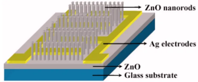
Before the device fabrication, 40-nm-thick ZnO seed layers were deposited onto glass substrates using radio fre-quency magnetron sputter deposition technique. Sequentially the as-grown ZnO films were annealed at 450 ° C for 30 min under oxygen ambience. 120-nm-thick Ag electrodes were subsequently deposited onto the ZnO film by electron beam evaporation to serve as Schottky contacts. The fingers of the Ag contact electrodes were 150 m long and 10 m wide with 10 m spacing. The active area of the whole device was 150⫻160 m2. Then we employed the photoresists in protecting the electrode patterns by lithography technique. The sample with photoresist-protected interdigitated elec-trodes was subsequently immersed in the Zn共NO3兲2/NH4OH aqueous solution for 4 h at 90 ° C. The fabricated MSM PDs were removed from the solution, rinsed with distilled water, and dried in air. Finally, we removed the photoresists from the interdigitated electrode surface of devices. The structure of ZnO NR MSM PD is shown in Fig.1. On the other hand, the traditional MSM PDs with 40-nm-thick ZnO film were fabricated for comparison, where no ZnO NRs can be found.
X-ray diffraction 共XRD兲, microphotoluminescence, and high-resolution transmission electron microscopy 共HRTEM兲 共JEOL JEM-3010兲 were then used to characterize the optical and crystallographic properties of the as-grown ZnO NRs. Surface morphologies of the NRs and NR PDs were charac-terized by a field-emission scanning electron microscope 共FESEM兲 共JEOL JSM-6700F兲. An HP-4156C semiconductor parameter analyzer was then used to measure current-voltage 共I-V兲 characteristics of the fabricated ZnO NR PDs. Spectral responsivity measurements were also performed by the TRAIX 180 system with a 300 W xenon arc lamp light source and a standard synchronous detection scheme.
Figure2共a兲shows the XRD and photoluminescence共PL兲 results共inset兲 of the as-grown ZnO NR arrays. It can be seen that the ZnO NRs with good crystal quality were preferred oriented in the 关002兴 c-axis direction and a strong UV emis-sion centered at 378 nm. In Fig.2共b兲, HRTEM and selective area electron diffraction 共SAED兲 pattern show the ZnO NRs is structurally uniform and contains no defects such as dis-locations and stacking with 0.52 nm d-spacing of共002兲 crys-tal planes.
A FESEM image with a 45° tilt angle of the ZnO NR PDs is as shown in Fig.3; the inset shows a cross-sectional photograph of the NR arrays. The average length and diam-eter of these ZnO NRs were around 2.2 m and 60–80 nm, respectively. It was found that high densities of well-aligned ZnO NR arrays were grown on the gap of interdigitated elec-trodes.
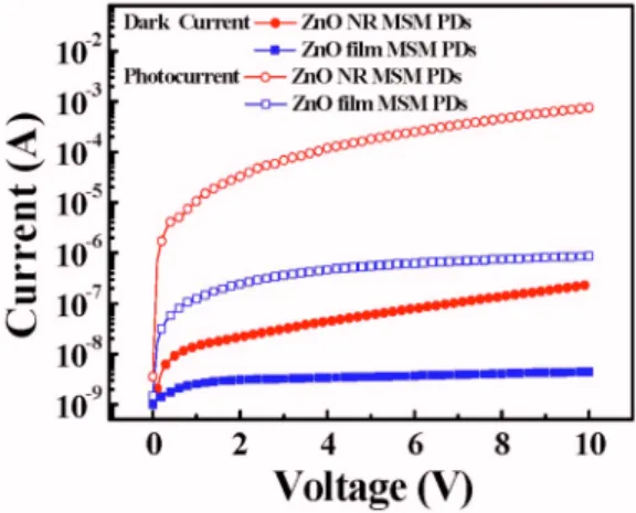
Figure 4 shows current-voltage 共I-V兲 characteristics of the fabricated traditional ZnO film and ZnO NR MSM PDs
a兲Author to whom correspondence should be addressed. Electronic
ad-dresses: lwji@seed.net.tw and lwji@nfu.edu.tw.
FIG. 1. 共Color online兲 Schematic for the fabricated UV MSM PDs with ZnO NR arrays.
APPLIED PHYSICS LETTERS 94, 203106共2009兲
0003-6951/2009/94共20兲/203106/3/$25.00 94, 203106-1 © 2009 American Institute of Physics
with the Ag interdigitated electrodes measured in dark and under 370 nm illumination. With 5 V applied bias, the pho-tocurrent to dark current contrast ratios of the ZnO and ZnO
NR PDs were 1.47⫻102 and 2.99⫻103, respectively. The photocurrents generated from NR MSM PDs are increased much more than the traditional film MSM PDs could be attributed to the NR arrays having larger surface area than film.
The spectral responsivities of the ZnO MSM PDs with 5 V applied bias were shown in Fig.5. It can be seen that the photoresponsivities were nearly constant in the UV region 共300–370 nm兲. UV-to-visible rejection ratio can be defined as the responsivity measured at 360 nm divided by the respon-sivity at 450 nm.4 Table I summarizes photo-/dark current, responsivities, UV-to-visible rejection ratios for ZnO NR, and ZnO film MSM PDs. The ZnO NR MSM PDs show much higher photoresponse than the traditional ZnO MSM PDs共41.22 A/W, 0.13 A/W兲 can be attributed to the defects of NR surfaces, which is the origin of the trap states, and the surrounding gas molecules completely affects energy band and produce photoconduction gain.10,11The responsivity of a detector, R, is defined as
R = Ip Pinc
=g共m兲
1.24 A/W,
where Ip, Pinc,, g, and are the photocurrent, the incident optical power, the quantum efficiency, the photoconductive gain, and the incident light wavelength, respectively.17While we apply 41.22 A/W and 370 nm to the expression, the gain can be estimated to be 1.38⫻102by assuming= 1 for sim-plicity. Such a result suggests that an internal gain exists in the NR device.10
FIG. 5. 共Color online兲 Measured spectral reponsivities of the ZnO MSM PDs at 5 V applied bias.
FIG. 2.共a兲 XRD result of ZnO NRs on ZnO/glass substrate. The inset shows the room temperature PL spectrum of ZnO NRs.共b兲 HRTEM image of an individual ZnO NR. The lattice spacing is 0.52 nm along the关002兴 direction. The inset is the corresponding SAED image.
FIG. 3. FESEM image with 45° tilt angle for the ZnO NR MSM PDs. The inset shows the cross-sectional image of the ZnO NR arrays.
FIG. 4.共Color online兲 I-V characteristics of the NR MSM PDs measured in dark and under 370 nm illumination.
203106-2 Ji et al. Appl. Phys. Lett. 94, 203106共2009兲
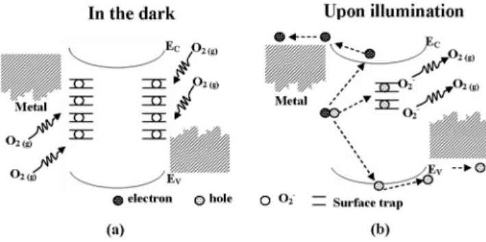
Figure6 shows a the energy band diagram in the pres-ence of a high density of hole-trap states at the NR surfaces. It is generally accepted that oxygen molecules are adsorbed onto the ZnO surfaces by capturing free electrons from the
n-type ZnO 关O2共g兲+e−→O2
−共ad兲兴, as shown in Fig. 6共a兲 , where a low-conductive depletion layer will be formed near the surface. The electron-hole pairs will be photogenerated 关h→e−+ h+兴 while the photon energy of illumination is more than the energy bandgap Eg关h⬎Eg, as shown in Fig.
6共b兲兴. The holes that migrate to the surface along the poten-tial gradient, produced by band bending, discharge the nega-tively charged adsorbed oxygen ions 关h++ O
2
−共ad兲→O 2共g兲兴; consequently, oxygen is desorbed from the surfaces, result-ing in an increase in the free carrier concentration and a decrease in the width of the depletion layer.9–11,18 In other words, the photoresponses of the NR MSM PDs are
en-hanced by the hole-trapping mechanism through oxygen ad-sorption and dead-sorption in ZnO NRs, which increases the density of trap states. Furthermore, this leads to an increase in carrier injection and transport, producing a persistent pho-tocurrent.
In summary, we investigated the UV MSM PDs with selectively grown ZnO NR arrays, which show higher pho-toresponse compared to the traditional ZnO MSM PD. As a result, it can be attributed to the very large surface-to-volume ratios of ZnO NR arrays easily promoting oxygen adsorption and desorption at the NR surfaces. Based on the trapping mechanism related to gas adsorption/desorption, it suggests that ZnO NRs are superior materials for UV detection.
This work was supported by the National Science Coun-cil of Taiwan under Contract No. NSC-95-2221-E-150-077-MY3.
1D. M. Bagnall, Y. F. Chen, Z. Zhu, T. Yao, S. Koyama, M. Y. Shen, and T.
Goto,Appl. Phys. Lett. 70, 2230共1997兲.
2D. C. Look, D. C. Reynolds, C. W. Litton, R. L. Jones, D. B. Eason, and
G. Cantwell,Appl. Phys. Lett. 81, 1830共2002兲.
3S. J. Young, L. W. Ji, S. J. Chang, and Y. K. Su,J. Cryst. Growth 293, 43
共2006兲.
4D. Y. Jiang, J. Y. Zhang, Y. M. Lu, K. W. Liu, D. X. Zhao, Z. Z. Zhang, D.
Z. Shen, and X. W. Fan,Solid-State Electron. 52, 679共2008兲.
5W. I. Park, D. H. Kim, S. W. Jung, and G. C. Yi,Appl. Phys. Lett. 80,
4232共2002兲.
6L. W. Ji, S. J. Young, T. H. Fang, and C. H. Liu,Appl. Phys. Lett. 90,
033109共2007兲.
7Y. Ryu, T. S. Lee, J. A. Lubguban, H. W. White, B. J. Kim, Y. S. Park, and
C. J. Youn,Appl. Phys. Lett. 88, 241108共2006兲.
8M. H. Huang, S. Mao, H. Feick, H. Q. Yan, Y. Y. Wu, H. Kind, E. Weber,
R. Russo, and P. D. Yang,Science 292, 1897共2001兲.
9H. Kind, H. Q. Yan, B. Messer, M. Law, and P. D. Yang, Adv. Mater. 共Weinheim, Ger.兲 14, 158共2002兲.
10C. Soci, A. Zhang, B. Xiang, S. A. Dayeh, D. P. R. Aplin, J. Park, X. Y.
Bao, Y. H. Lo, and D. Wang,Nano Lett. 7, 1003共2007兲.
11Y. Z. Jin, J. P. Wang, B. Q. Sun, J. C. Blakesley, and N. C. Greenham, Nano Lett. 8, 1649共2008兲.
12H. T. Ng, T. Yamada, P. Nguyen, Y. P. Chen, and M. Meyyappan,Nano Lett. 4, 1247共2004兲.
13K. Keem, D. Y. Jeong, S. Kim, M. S. Lee, I. S. Yeo, U. I. Chung, and J. T.
Moon,Nano Lett. 6, 1454共2006兲.
14J. B. Baxter and E. S. Aydil,Appl. Phys. Lett. 86, 053114共2005兲. 15X. D. Wang, J. H. Song, J. Liu, and Z. L. Wang,Science 316, 102共2007兲. 16Q. Wan, Q. H. Li, Y. J. Chen, T. H. Wang, X. L. He, J. P. Li, and C. L. Lin,
Appl. Phys. Lett. 84, 3654共2004兲.
17S. M. Sze, Physics of Semiconductor Devices共Wiley, New York, 1981兲. 18P. Sharma, K. Sreenivas, and K. V. Rao,J. Appl. Phys. 93, 3963共2003兲.
TABLE I. Photocurrent, dark current, photoresponsivity, and UV-to-visible rejection ratio of the ZnO MSM PDs measured at 5 V bias and 370 nm illumination. Photo-/dark current Responsivity 共A/W兲 UV-to-visible rejection ratio ZnO NRs 0.18 mA/60.3 nA 41.22 336.65
ZnO film 552 nA/3.55 nA 0.13 28.28
FIG. 6. Energy band illustration for photoconduction mechanism in this investigation:共a兲 In the dark case, oxygen molecules are adsorbed onto the ZnO surfaces by capturing free electrons关O2共g兲+e−→O2−共ad兲兴, which
cre-ates a low-conductivity depletion layer near the surface.共b兲 Under UV illu-mination at photon energy more than the bandgap共h⬎Eg兲, electron-hole
pairs are photogenerated. The holes migrate along the potential gradient and discharge the oxygen ions关h++ O
2 −共ad兲→O
2共g兲兴, consequently, oxygen is
photodesorbed from the surfaces.
203106-3 Ji et al. Appl. Phys. Lett. 94, 203106共2009兲