國立臺灣大學電機資訊學院電信工程學研究所 碩士論文
Graduate Institute of Communication Engineering College of Electrical Engineering and Computer Science
National Taiwan University Master Thesis
基於剪切模態體聲波激發之多鐵電性天線 之寬頻極化控制
Broadband Polarization Control of
Bulk Acoustic Wave-Mediated Multiferroic Antenna Based on Thickness Shear Modes
許瑞福 Rui-Fu Xu
指導教授:陳士元 博士 Advisor: Shih-Yuan Chen, Ph.D.
中華民國 108 年 7 月
July, 2019
誌謝
能完成這篇論文,真的非常不容易。首先我要特別感謝我的指導教授陳士元老
師,以及遠在UCLA 的 Rob Candler 老師。在偶然的機會之下,兩位教授引領我進
入學術的殿堂,非常有耐心地討論並給予意見,才能讓我有機會研究最前沿的知識 及題目,挑戰重大的科技問題。陳士元老師總是能給予有用且正向的回饋,激盪腦
力讓我的研究得以不斷地前進,是我學術上最好的典範及學習的對象。而 Rob
Candler 教授在台灣訪問的約一年間,總是不吝嗇地分享想法及提供建議,讓我有
機會探索知識的邊界。我也要感謝UCLA 的博士生 Sidhant Tiwari,在這三年間不
間斷地透過電子郵件討論並交換學術意見。雖然這個題目因為非常前沿,加上橫跨 許多領域,因此時常討論並無確切結論,但他還是盡力協助回答,並花了一整年的 時間將我的晶片實作出來。天線實驗室的廖修平學長、Robin 學長、聖偉學長、登 胤學長,也給予我在量測及模擬上許多的意見與協助,若沒有他們的協助很難完成 地這麼順利。也很感謝實驗室的同學們紫瑀、奕霖、金隆,大家時常提供給我不同 的想法及刺激,若這麼新的題目缺乏討論,實在是很在進行下去。也謝謝我研究所 期間兩年的陸生室友王達,讓我在苦悶的論文撰寫期間多了不少樂趣。也要感謝我 的父母,他們從小到大無條件愛我並讓我成長,才讓我有機會追求學術的夢想。最 後我希望感謝鄭明析牧師,他透過聖經的教導讓我深刻了解基督信仰,在對信仰的 追求及努力之下,也讓我決心走上追求挑戰及創新的學術之路,更有力量能堅持下 去不放棄。這個題目做得人很少也很新,與此同時研究所這三年我卻同時擔任了行 政院青年諮詢委員、台大研究生協會會長,每週開大大小小的會議,辦了數十場研 究生的活動,也到了英特爾實習,若沒有信仰的力量我無法做到這麼多事情,擁有 這麼精采的研究所生活。真心期盼未來能將學術的果實貢獻於台灣社會全體,幫助 改善人類的生活,充實台灣的國家實力能更加獨立且茁壯。
中文摘要
近年來在5G、物聯網、生醫電子、穿戴式裝置等應用的發展之下,天線微小
化已逐漸成為越來越重要的題材。天線微小化在過往有許多的嘗試,例如:使用高 磁導率或是介電係數的基材、不同的天線設計等等。但不論在低頻或高頻頻段,只
要天線相對於共振波長尺寸遠小於一時,輻射效率就會變得很差而不堪使用。2015
年首次提出了利用機械聲波,採用多鐵電性材料來實現天線微小化的可能性,基本 原理是機械聲波在相同的共振頻率下,波長相較電磁波小了千倍到萬倍左右,因此 若能在合適的共振頻段減少耗損,將有可能實現天線微小化並逼近理論極限。然而 在過往提出的設計概念中,主要是使用縱向波的共振來實現,在本研究中主要針對 了這類型新的天線,首次提出了藉由平面電極來激發剪切模態的概念。因為剪切模 態可以有對稱且相互垂直的兩個模態,因此若施加特定相位差將可進行極化控制。
除了極化控制之外,剪切模態可激發橫向的磁流,因此若放置於金屬平面上,可期
待得到更強而非相消的輻射。此類極化控制的設計概念,使用了COMSOL 數值模
擬及MATLAB 的後處理計算來驗證。根據模擬結果在理想的九十度相位差饋入之
下,此類圓極化模態擁有極寬頻的特性。相關設計由UCLA 的 Rob Candler 教授之
研究團隊製作晶片並在台大完成了量測,本論文亦將針對量測結果進行初步的探 討與分析。
ABSTRACT
Antenna miniaturization has been more and more important these days. Many applications like IOT, biomedical devices, wearable devices, and 5G demand higher performance with smaller feature size. Many works on antenna miniaturization have been done before, such as using substrate with high permittivity or permeability, diverse structure antenna design, etc. However, no matter in UHF or VLF band, as long as the electrical size of an antenna is much smaller than one, the radiation efficiency will be extremely low, making the antenna infeasible. In 2015, theoretical groundwork of using multiferroic material to achieve antenna miniaturization was firstly propose, named “bulk acoustic wave-mediated multiferroic antenna”. The core concept is that the wavelength of mechanical wave is five orders of magnitude smaller than electromagnetic wave under the same resonant frequency. As long as the loss can be further reduced, it owns great potential to approach Chu’s limit for electrically small antennas.
In the above mentioned works, the radiation is mainly generated based on longitudinal acoustic wave. In this thesis, thickness shear mode is used instead of longitudinal one. By using the shear mode, two sets of symmetrical but orthogonal resonant modes can be manipulate by applying 90 phase difference to generate circularly polarized (CP) wave. In addition, the shear wave can excite in-plane magnetic current, which will double the radiation instead of cancelling out each other when the device is placed above a metallic ground plane according to the image theory. Such concept can also be used for tunable polarization control. The design concept is preliminarily investigated through FEM-based multi-physics solver, COMSOL, and post processing by an in-house MATLAB code. It is shown that under the ideal input RF signal pair of equal magnitude and with 90° phase difference, the proposed design can achieve very
broadband CP with satisfactorily low in-band axial ratio. The design is fabricated by Dr.
Sidhant Tiwari from UCLA. The test pieces were tested, and the results thus obtained are presented and discussed through a couple of comparisons. This work envisions the possibility of broadband polarization control and/or tunability of electrically small antennas.
CONTENTS
口試委員審定書 ... ii
誌謝 ... iii
中文摘要 ... iv
ABSTRACT ... v
CONTENTS ... vii
LIST OF FIGURES ... ix
LIST OF TABLES ... xvi
Chapter 1 Introduction ... 1
1.1 Evolution of Mobile Standards from 1G to 5G ... 1
1.2 RF MEMS as a Potential Boosting Technology to RF System Improvement 8 1.3 Brief Review on Antenna Miniaturization Theory ... 14
1.4 Applications for Miniaturized Antenna ... 20
Chapter 2 Background and theory ... 28
2.1 Piezoelectric and Magnetic Material for Microwave Application ... 28
2.2 Dynamic Magnetization as a Radiation Source ... 37
2.3 Sources of Dynamic Magnetization... 40
2.4 Device Operation Principle... 46
Chapter 3 Circularly-polarized BAW Multiferroic Antenna ... 49
3.1 Circular Polarization Control of Bulk-Acoustic Wave Medieated Antenna Using Lateral Field Excitation ... 49
3.2 Numerical modelling ... 53
3.3 Results and Analysis ... 57
Chapter 4 Measurement results ... 70
4.1 Device fabrication and design ... 70
4.2 Setup and measurements... 79
4.3 Results and Discussions ... 84
Chapter 5 Conclusions ... 87
5.1 Summary ... 87
5.2 Future Works ... 88
References ... 89
LIST OF FIGURES
Fig. 1.1. First portable device for mobile radio communications [1] ... 1 Fig. 1.2. Trend in size reduction of mobile handsets [3]. ... 2 Fig. 1.3. Flywheel effect triggering more and more data demand from the end user side [7]. ... 4 Fig. 1.4. Comparison of maximum data rate capacity, in terms of Mbps [6]. ... 4 Fig. 1.5. Trend in the decrease of connection quality [8]. ... 6 Fig. 1.6. Performance bowl for the most significant specifications and characteristics expected from RF passives for 5G applications [9]... 6 Fig. 1.7. Plot of crossed-relationships among 5G challenges, facilitators and design trends [10]. ... 7 Fig. 1.8. Prediction of number of components per chip. Historical data from 1959 to 1965 and Moore’s extrapolation after 1965 [11]. ... 8 Fig. 1.9. Photos of some MEMS inertial sensors. (a)–(e): MEMS acceleration sensors, (a) first type of integrated acceleration sensor (1-axis); (b), (c) 2-axes; and (d), (e) 3-axes sensors. (f)–(h): MEMS gyros (f), (g): 1-axis, (h): 2-axes [16]. .. 10 Fig. 1.10. Typical hype curve behavior elaborated by Gartner Inc. [20]. ... 11 Fig. 1.11. Evolution of RF-MEMS market forecasts released in: (a) 2004; (b) 2006; (c) 2010; (d) 2012; (e) 2013 [21]. ... 13 Fig. 1.12. Antenna within a sphere of radius r, and its equivalent circuit model [25]. ... 14 Fig. 1.13. Measured product for 110 antenna designs published in the IEEE T-AP by the end of 2010 [26]... 17 Fig. 1.14. ME FBAR antenna demonstrated in [36]. The longitudinal mode is excited and the radiation at 2.5GHz is detected with comparison of FeGaB to Al material.
... 19
Fig. 1.15. Technology roadmap of Internet of Things (IOT) [44] ... 20
Fig. 1.16. The components of a RFID system ... 21
Fig. 1.17. Evolution of RFID tags compared in size to a penny from 12 bits to 1024 bits. The area of the circuitry of the tag has been reduced greatly except the area occupied by antenna [46]. ... 22
Fig. 1.18. Implant with antenna and circuitry [47] ... 24
Fig. 1.19. Dual band antenna [47] ... 24
Fig. 1.20. Photos of prototypes and nonwoven conductive fabrics (NWCFs) [53]. ... 25
Fig. 1.21. Underground communications [34] ... 26
Fig. 1.22. Underwater communications [34] ... 26
Fig. 1.23. Attenuation of EM wave passing through Sea Water [56] ... 27
Fig. 1.24. US Navy’s VLF antenna in Cutler, Maine [34] ... 27
Fig. 1.25. Spinning Magnet Array [34] ... 27
Fig. 2.1. Concept illustration of a piezoelectric disk generating a voltage when deformed. ... 28
Fig. 2.2. Comparison of a classical LC TV IF filter with an SAW TV IF filter [62] ... 31
Fig. 2.3. Application space regarding frequency spectrum or RF filters [63] ... 32
Fig. 2.4. (a) FBAR and (b) SMR structures. [65] ... 33
Fig. 2.5. Example BAW filters used in iPhone 6(EPFL online course MEMSx). ... 33
Fig. 2.6. Photograph of a disassembled ferrite junction circulator, showing the stripline conductor, the ferrite disks, and the bias magnet. [69] ... 35
Fig. 2.7. BAW-resonance-based antenna [36]. ... 36
illustrating different types of coupling present in materials [71]. ... 36 Fig. 2.9. Spin magnetic dipole moment and angular momentum vectors for a spinning Electron [69]. ... 40 Fig. 2.10. Magnetic moment of a ferrimagnetic material versus bias field 𝐻0 [69]. .... 42 Fig. 2.11. Dynamic permeability in the vicinity of FMR (a) Magnitude of permeability.
(b) Real and imaginary parts of the permeability [72]. ... 44 Fig. 2.12. SAWs are generated in a piezoelectric substrate by applying an AC ... 45 Fig. 2.13. (a) Plot of the absorption of SAW power by the magnetic element (in dB) as a function of applied x and y magnetic field at a SAW frequency of 1992 MHz (b) Line cut along the direction indicated by the black line in (a) at a number of different SAW frequencies (green, 857 MHz; red, 1424 MHz; and black, 1992 MHz). [74] ... 45 Fig. 2.14. FDTD modelling of proposed antenna structure by Zhi Yao et al. First column is the excited acoustic resonance mode. Middle column is the stress profile as a function of time. Last column is the radiated electric field [37]. ... 46 Fig. 2.15. BAW resonance based antenna. (a) Structure and physical coupling mechanism.
(b) Cross section of the antenna. Electric current excitation is applied to the electrodes to drive bottom piezoelectric layer, and the standing wave resonance further triggers the magnetostrictive layer as the equivalent magnetic current source of radiation [37]. ... 48 Fig. 3.1. (a) Left-hand circular polarization. (b) Right-hand circular polarization. (c) Polarization ellipse [77]. ... 51 Fig. 3.2. The sketch of the AlN-based solidly mounted resonator operated in thickness shear mode waves [79] ... 51 Fig. 3.3. Electric and magnetic sources and their images near electric (PEC) and ... 52
Fig. 3.4. The finite element simulation of the electric field generated by the simple ... 52 Fig. 3.5. Simulated structure of BAW-mediated multiferroic antenna. M represents magnetization inside magnetostrictive layer. ... 53 Fig. 3.6. Two sets of lateral electrodes are placed at the bottom of BAW-mediated multiferroic antenna. Each set of electrode includes a terminal connected to ground and a terminal connected to voltage source. The spacing between two terminals of one set of electrodes is 10 (μm). The thickness of electrodes is 0.1 (μm). External voltage sources with 90-degree phase differences are applied upon each set of electrodes and thus creates circular polarized electric field at the bottom. ... 54 Fig. 3.7. Flow chart of numerical modelling. ... 57 Fig. 3.8. Snapshots of displacement animation operated at 250 MHz (length units in μm).
(Left-top) t =T/4; (Right-top) t=T/2; (Left-bottom) t=3T/4; (Right-bottom) t=T. Counter-clockwise circular polarized (from top’s view) displacement can be observed clearly. ... 59 Fig. 3.9. Magnitude and phase distribution across z axis of stress tensor (a) Left: Txz and (b) Right: Tyz insides the device. ... 61 Fig. 3.10. (a) X-Z cut radiation pattern; (b) Y-Z cut radiation pattern. Radiation pattern of circular polarized BAW-mediated multiferroic antennas. This calculated radiation pattern is selected to be the frequency with lowest axial ratio within simulated frequency range. ... 62 Fig. 3.11. Broadside axial ratio versus frequency between 100MHz and 500MHz. ... 62 Fig. 3.12. Resonant mode 1 at 148MHz with axial ratio = 0.16. It is identified as weak
Fig. 3.14. resonant mode 2 at 249MHz with axial ratio = 0.12. ... 64 Fig. 3.15. Resonant mode 2 at 249MHz with axial ratio = 0.12. It is identified as main desired fundamental thickness shear modes. ... 64 Fig. 3.16. Resonant mode 3 at 387MHz with axial ratio = 8.9. ... 65 Fig. 3.17. Resonant mode 3 at 387MHz with axial ratio = 8.9. It is identified as the excitation of undesired mode. ... 65 Fig. 3.18. Resonant mode 4 at 472MHz with axial ratio = 0.31. ... 66 Fig. 3.19. Resonant mode 4 at 472MHz with axial ratio = 0.31. It is identified as the second order of thickness shear mode. ... 66 Fig. 3.20. Resonant mode 5 at 476MHz with axial ratio = 10.6. ... 67 Fig. 3.21. Resonant mode 5 at 476MHz with axial ratio = 10.6. It is identified as the excitation of undesired mode. ... 67 Fig. 3.22. The magnitude and phase distribution along z axis of radius of 1μm. The axial ratio of frequency responses is also shown... 68 Fig. 3.23. Simulated structure of thickness of 1.1μm and radius of 1μm. ... 68 Fig. 3.24. The magnitude and phase distribution along z axis of radius of 10μm. The axial ratio of frequency responses is also shown... 69 Fig. 3.25. Simulated structure of thickness of 1.1μm and radius of 10μm. ... 69 Fig. 4.1. Fabrication process of BAW antenna [72]. ... 70 Fig. 4.2. Layout of 200 μm CP BAW antenna. The green pads represent electrodes. The blue lines represent electric trace to provide shear excitation. The red disk represents the fabricated BAW antenna. ... 72 Fig. 4.3. Layout of 500 μm CP BAW antenna. The green pads represent electrodes. The blue lines represent electric trace to provide shear excitation. The red disk represents the fabricated BAW antenna. ... 73
Fig. 4.4. Layout of 1000 μm CP BAW antenna. The green pads represent electrodes. The blue lines represent electric trace to provide shear excitation. The red disk represents the fabricated BAW antenna. ... 73 Fig. 4.5. Four ports CPW-Slot-CPW wideband branch-line coupler ... 74 Fig. 4.6. Simulated S parameters of four ports CPW-Slot-CPW wideband branch-line coupler connected with SMA connectors. ... 75 Fig. 4.7. Photo of the finished four ports wideband CPW-Slot-CPW branch-line coupler... 75 Fig. 4.8. Finished CP BAW antenna soldered onto branch-line coupler. ... 76 Fig. 4.9. Feeding BAW antenna and connecting with later electrodes with port 2 and 376 Fig. 4.10. Photo of the fabricated BAW antenna of 500μm. ... 77 Fig. 4.11. Photo of the fabricated BAW antenna of 1000μm one under optical microscope.
The bond wires are used to connect with CPW signal and ground. The device is in the center of the chip. ... 77 Fig. 4.12. Photo of the fabricated BAW antenna of 200μm. ... 78 Fig. 4.13. Block diagram of measurement setup ... 80 Fig. 4.14. Measurement setup. Network analyzer at the right position is connected to horn antenna. A tunable permanent magnet is place the bottom to provide external biased magnetic field to saturate the device. ... 80 Fig. 4.15. he adjustable permanent magnet is meant to provide necessary out-of-plane magnetic field to saturate the device. One tesla is measured near the surface of the chip using a DC magnetic meter MG-3003SD. ... 81 Fig. 4.16. The photo of fabricated patch antenna. ... 81
Fig. 4.19. Measuring radiation from four ports coupler itself. The coupler is placed at the same direction with the col-pol of patch antenna. By rotating the coupler by 90 degrees relative to the center of the magnet(red cross in the figure), the orthogonal component which is the same as cross-pol of patch antenna can be measured. ... 83 Fig. 4.20. The measured S parameters of CP BAW antenna of Ni/NiFe with radius of 200μm. ... 85 Fig. 4.21. The measured S parameters of patch antenna/branch-line coupler/coupler connected with load. ... 85 Fig. 4.22. The measured S parameters of CP BAW antenna of Ni/NiFe with radius of 1000μm. ... 86 Fig. 4.23. The measured S parameters of CP BAW antenna of Ni/NiFe with radius of 500μm. ... 86
LIST OF TABLES
Table 1. Summary of mechanical antenna transmitter experiments [33]. ... 18
Table 2. Piezoelectricity, innovation fields, and important applications [61] ... 30
Table 3. Basic parameters of COMSOL simulation ... 58
Table 4. Fabrication process of BAW antenna for each layer and action. ... 71
Chapter 1 Introduction
1.1 Evolution of Mobile Standards from 1G to 5G
In 1885, the electromagnetic wave experiment conducted by German physicist Heinrich Hertz first unveiled the era of wireless communication. Since then, the demands on hardware capabilities of mobile systems have been gradually elevated. In Fig. 1.1, the first portable device for mobile radio communications (i.e., a radio signal strength testing system) in 1924 is shown. It was quite bulky and very different from the outlooks of modern handsets. It was not until 1979, the first commercial cellular network for voice transmission started, covering more than 20 million users of Tokyo. At then, so-called
“mobile” handset seemed still not so “mobile”. Power consumption is extremely high.
It’s even not an affordable option for a common household. In Fig. 1.2, the great advances
Fig. 1.1. First portable device for mobile radio communications [1]
of significant size reduction of mobile handset can be observed [1].
Right after the birth of wireless communication, the second mobile networks (2G) continued spreading the mobile services to larger numbers of people. Compared to 1G, 2G focused on dealing with digital signal processing. Bitrate can be reduced from 64 kb to 8 kb per second after encoding the voice signal. With the introduction of Global Systems for Mobile communications (GSM), the available channels are expanded greatly and the first non-voice data, by means of Short Message Service (SMS) and e-mail exchange was launched [2].
After many important breakthroughs accomplished, 2G was followed by 3G in 2000.
After the introduction of 2G service, users are becoming more eager for broadband usage and wider coverage of mobile services. These factors drove huge increase of the demand of mobile Internet. The trends of growing needs for higher data rates is shown in Fig. 1.3.
However, this means that not only RF systems and transmission data capabilities but also relative components integrated in device require a huge advancement, e.g., camera and
screens, etc.
4G Long Term Evolution (4G- LTE) is not an exception following the same trends of expanding system capacities 錯誤! 找不到參照來源。. More and more services are integrated with the 4G standards, which all demand faster and more efficient data transfer.
New techniques like Carrier Aggregation (CA) and Multiple Input Multiple Output (MIMO) were introduced for the sake of above-mentioned needs [4]. The relation between user demand and system performance is illustrated in Fig. 1.4.
From the above reviews, it’s quite natural to think that the 5th generation (5G) aims to provide more advanced system capacities, such as higher data transfer capacity and wider coverage, etc. In addition to that, it’s also expected to provide interconnected services for wireless connections. Hence the Internet of Things (IoT) paradigm is proposed, aiming to picture the futuristic digital world based on these concepts. The IoT is based on the following functionalities [5]:
• Self-awareness. Served as identification, localization and self-diagnosis of the object environment;
• Interaction with the surrounding environment. Emphasizing on data acquisition (sensing and metering) and actuation;
• Data elaboration. Interpreting or analyzing for both basic (primitive data aggregation) and advanced (statistics, forecasts).
There are several application areas mentioned frequently like Smart City/Environment, Smart Home, Smart Metering/Smart Grid, Smart Building, eHealth,
Fig. 1.4. Comparison of maximum data rate capacity, in terms of Mbps [6].
Fig. 1.3. Flywheel effect triggering more and more data demand from the end user side [7].
Everything (IoE), which includes much more applications, such as Virtual Reality (VR), Augmented Reality (AR), Machine to Machine (M2M) communication and the Tactile Internet. Hence, the transmission capacity in 5G is expected to be 1000 times faster than 4G-LTE, equivalent to 10 Gbps to each user. Some applications like Vehicle to Vehicle (V2V) communications will require extra features, such as extremely low latency. These challenges are named as EMBB (Enhanced Mobile Broadband), URLLC (Ultra-Reliable Low-Latency Communications) and MMTC (Massive Machine-Type Communications) as discussed in [5].
One of the important approach is the mmWave usage. Sub-6 GHz or well above 6 GHz (up to 60–70 GHz) spectrum usage are extensively discussed, combining massive MIMO solutions and advanced beamforming capabilities. However, as mobile devices become smaller and thinner, it has been a tough and challenging task to improve overall performances simply by integrating circuitry. In [8], it is estimated that the theoretical ratio of signal quality versus actual RF signal quality was decreasing with a pace of about 1 dB per year for over a decade. This is an inevitable problems for all RF engineers since performances of RF system and the services quality provided will be greatly undermined (see Fig. 1.5). RF MEMS is anticipated to be one of the potential saviors for these imminent challenges. The commonly mentioned problems faced by 5G system implementation are listed in Fig. 1.6. Theses 5G challenges of RF systems are summarized in Fig. 1.7.
Fig. 1.5. Trend in the decrease of connection quality [8].
Fig. 1.6. Performance bowl for the most significant specifications and characteristics expected from RF passives for 5G applications [9].
Fig. 1.7. Plot of crossed-relationships among 5G challenges, facilitators and design trends [10].
1.2 RF MEMS as a Potential Boosting Technology to RF System Improvement
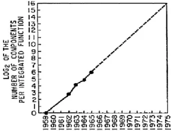
In 1965, an article entitled “Cramming more components onto integrated circuits”
marks an indelible moment in human history. It was this review that firstly investigate the progress in the semiconductor industry [11]. Moore observed that the number of components per chip was roughly doubling every year since the invention of the first commercial transistor in 1959. Based on this observation, he proposed a bold statement, predicting the exponential growth in circuit density. This trend of the growth of components per chip seems to be “a life without tradeoffs” with the benefits of continuous reduced cost per transistor [12]. With the tremendous efforts of countless engineers, these three factors of advancement completely revolutionized the whole integrated circuit (IC) industry and our daily life. For the past 40 years, the number of transistors on a semiconductor device has doubled approximately every 18–24 months. The cost reduced about 25-30% per year, giving birth to many complex, high performance, and low power products. If you spend $1 to buy a transistor in 1965, you can almost buy 10 million
Fig. 1.8. Prediction of number of components per chip. Historical data from 1959 to
transistors now [13].
With the prosperous success in IC industry, the manufacturing process continued to refine and become mature. In 1982, K. Peterson published a widely-cited paper, analyzing the potential of silicon as mechanical material [14]. There are four important traits of silicon to be used as electronic base material, which greatly facilitates commercial success:
(1) low price/abundance; (2) processing based on thin deposited film amenable to miniaturization; (3) production using photographic techniques capable of high precision and amenable to miniaturization and; (4) able to be fabricated in batch [14]. As a result, silicon processing successfully finds new areas of applications and leads to various useful MEMS commercial products.
The concept of Micro-electromechanical system (MEMS) technology can be traced back to 1954 with the paper by Smith [15]. After the paper by Smith, MEMS technology has been successful used in many sensing devices, such as accelerometers, strain gauges, microphones, air mass flow sensors, pressure sensors, gyroscopes and yaw-rate sensors [15]. In Fig. 1.9, there’re several typical MEMS inertial sensors listed.
Compared to conventional MEMS products, RF passive component with MEMS technology is new. The first one came out in the early 1990 when MEMS accelerometers were valuable commercial products already. Coplanar waveguide (CPW) and microstrip implementations of transmission lines were studies first. Gradually there were more and more RF components added to the list of RF-MEMS applications. MEMS provides the potential to miniaturize RF passive components, such as switches, voltage-tunable capacitors, high-Q inductors, film bulk acoustic resonators (FBARs), dielectric resonators, transmission line resonators and filters, and mechanical resonators and filters, which mostly outperform traditional RF components if the cost is not considered [17]. Hence, it’s likely for RF-MEMS to revolutionize the design of the transceiver systems and be expected to solve the serious challenges for the implementation of 5G systems.
There are quite a few components of RF-MEMS anticipated to empower the 5G potential application scenes, especially for the mmWave band listed in [18]: “(1) Very- Fig. 1.9. Photos of some MEMS inertial sensors. (a)–(e): MEMS acceleration sensors, (a) first type of integrated acceleration sensor (1-axis); (b), (c) 2-axes; and (d), (e) 3- axes sensors. (f)–(h): MEMS gyros (f), (g): 1-axis, (h): 2-axes [16].
OFF) and very-low adjacent channels cross-talk, working from 2–3 GHz up to 60–70 GHz; (2) Reconfigurable filters with very good stopband rejection characteristics and extremely low attenuation of the passed band; (3) Very-wideband multi-state impedance tuners; (4) Programmable step attenuators with multiple configurations and very flat characteristics over 60–70 GHz frequency spans; (5) Very-wideband multi-state/analogue phase shifters; (6) Hybrid devices with mixed phase shifting and programmable attenuation; (7) Miniaturized antennas and arrays of antennas, integrated monolithically with one or more of the devices.”
The potential market growth is also discussed in [19]. According to the hype curve behavior proposed by Gartner Inc., the trends of new technologies, including RF-MEMS, are depicted in Fig. 1.10, and the market expectation for RF MEMS market from 2004- 2013 is shown in Fig. 1.11. Despite several overestimations occurred before, RF-MEMS still finds its market position gradually. Qorvo made more than quadruple of its RF- MEMS sales from 145 $M to 585 $M from 2014 to 2017. Through integrating RF-MEMS switches within RF front ends to increase re-configurability over Wi-Fi, Bluetooth, and cellular bands belonging to 3G and 4G networks, tremendous commercial success is
Fig. 1.10. Typical hype curve behavior elaborated by Gartner Inc. [20].
achieved. However, antenna is one of the key components which is rarely investigated in the field of RF-MEMS previously. Combined with the trends of 5G development and various applications, which will be discussed later, it can be expected that antenna miniaturization will play more and more important role. Before going into practical applications and design examples, antenna miniaturization theory will be briefly reviewed in the upcoming part.
Fig. 1.11. Evolution of RF-MEMS market forecasts released in: (a) 2004; (b) 2006; (c) 2010; (d) 2012; (e) 2013 [21].
1.3 Brief Review on Antenna Miniaturization Theory
Regarding how the fundamental limits of electrically small antennas were achieved, many theoretical works have been done. The approach to analyze such an issue was firstly investigated in Chu’s pioneer paper published in 1948 and quickly followed by Harrington and Wheeler in [22], [23] and [24]. The limits on electrically small antennas are studied firstly by assuming that the entire antenna structure within a sphere of radius r as shown in Fig. 1.12(a), sometimes known as “Chu sphere.” Based on the concept of
Chu sphere, electrically small antennas (or ESAs) are often defined as an antenna that satisfies the condition kr < 1, where k is the wave number 2𝜋
𝜆. The space outside the sphere was replaced by a number of independent equivalent circuits as shown in Fig.
Fig. 1.12. Antenna within a sphere of radius r, and its equivalent circuit model [25].
1.12(b). For a lossless antenna, a single network section with a series C and a shunt L is identified as the equivalent circuit of each spherical mode [25]. Hence, the combined circuit can be seen as a ladder network of L − C sections (one for each mode) with a shunt resistive load, as shown in Fig. 1.12(c). The resistive load represents the normalized antenna radiation resistance, and the original antenna space problem can now be simplified as a circuit problem.
In addition to theoretical investigation, there are some works trying to examine the validity and existence of Chu limit. In the paper by Daniel F. Sievenpiper et al., the previous theoretical works are reviewed and measurement results are compared based on specific criteria [26]. To start, Q is defined as the ratio of stored energy W to radiated power P at a particular frequency ω for an otherwise lossless antenna,
Q = ω𝑊
𝑃 1.3.1
where W is defined as
W = 2Max(𝑊𝑚, 𝑊𝑒) 1.3.2
𝑊𝑚 and 𝑊𝑒 and are the time-average, non-propagating, stored magnetic and electric energy. Hansen [27] and later McLean [28] derived an expression for Q of the lowest order mode in terms of the electrical size of the antenna’s
Q = 1 + 2(𝑘𝑎)2
(𝑘𝑎)3[1 + (𝑘𝑎)2]≅ 1
(𝑘𝑎)3 𝑤𝑖𝑡ℎ 𝑘𝑎 ≪ 1 1.3.3 Collin and Rothschild [29] calculated the energy associated with radiation from the total energy to find expressions for Q of each mode. The value for the lowest order spherical mode is given by
Q = 1
𝑘𝑎+ 1
(𝑘𝑎)3 1.3.4
In Fante’s work [30], he investigated gain and Q optimization including numerical results
for maximum G/Q. Yaghjian and Best [31] derived the relationship between B and Q through the maximum allowable voltage standing wave ratio VSWR, or s
Bandwith ≈ 1
𝑄(𝑠 − 1
√𝑠 ) 1.3.5
s = 2, Q = 1
√2𝐵−10𝑑𝐵 1.3.6
Since the radiation efficiency is always smaller than 1 and combined with 1.3.3, we can obtain the theoretical upper bound of the bandwidth-efficiency product
𝜂 ∙ Bandwith−10𝑑𝐵 <(𝑘𝑎3)
√2 1.3.7
The bandwidth efficiency products versus the electrical size for various published designs were shown in Fig. 1.13 [26]. The curves represents the theoretical limit that is derived by applying 1.3.5 to 1.3.4 using a VSWR of s = 2 and including efficiency
B𝜂 = 1
√2( 1
𝑘𝑎+ 1
𝑛(𝑘𝑎)3)−1 1.3.8
where n = 1 for linearly polarized or single-mode antennas, and n = 2 for circularly polarized or dual-mode antennas. It was found that most of the works follow the Chu limit except the one done by Friedman in [32]. However, it was due to the extra matching circuit and the incomplete measurement data.
From the above discussion, we know that it’s inevitable to face theoretical limit and need to tradeoff between bandwidth and efficiency while trying to miniaturize the antenna.
What makes it worse is that traditional antennas adopted for miniaturized component, such as dipole, loop, or patch, struggle with image current effect as well as excessive storage of reactive energy between the radiating element and ground, not to mention ohmic losses. These effects will increase the radiation Q factor, make the antenna difficult to match and essentially kill the radiation efficiency. Hence, there are several works aiming at proposing innovative structure different from traditional one. They try to use mechanical resonance coupled with multiferroic material as the source of electromagnetic radiation. In 2019, the group of Draper Laboratory in Cambridge coined the name of
“mechanical” and “antenna” as “mechtenna” [33]. The basic concept is that mechanical Fig. 1.13. Measured product for 110 antenna designs published in the IEEE T-AP by the end of 2010 [26].
acoustic wave speed are typically several thousands (m/s). However, the speed of light in free space is in the order of 8 (m/s). Assuming that they’re both operating under the same resonant frequency, the mechanical resonant structure can be miniaturized by about the order of 5, which is fundamentally different from conventional one. Various kinds of
“mechtenna” are proposed based on different operational frequencies, integrating diverse antenna structures listed in Table 1. For example, an design for ULF band (300 Hz to 3000 Hz) was studied in [34] and that for UHF (300 MHz to 3 GHz) was discussed in [35], [36]. For UHF band, Zhi Yao proposed a theoretical framework based on FDTD Multiphysics numerical simulation and calculated theoretical lower bound of quality factor of such an antenna in 2015. It was found that this kind of antenna has the potential to approach the Chu limit even down to the size of ka ≪ 1 at the frequency of 1 GHz [35] - [43]. In [36], they firstly measure the RX/TX behavior based on nanoplate resonators (NPR) at around 60 MHz and circular resonating disk made of FeGaB at around 2.5 GHz with the device diameter of only 200 μm, as shown in Fig. 1.14. They Table 1. Summary of mechanical antenna transmitter experiments [33].
However, in Zhi Yao’s framework, ferromagnetic resonance is used to explain magnetoelectric coupling, which indeed requires an external biased magnetic field.
Related research is still relatively new and in need of further study. In [36], it lacks explicit theoretical framework despite of evidences of experiments. Hence, I will still mainly follow the theoretical framework by Zhi Yao in the next sub chapter. This thesis is essentailly based on Zhi Yao’s structure and firstly tries to achieve polarization control with an innovative structure [41]. Before illustrating the operating principle of such devices, let’s look at several potential applications for such an antenna.
Fig. 1.14. ME FBAR antenna demonstrated in [36]. The longitudinal mode is excited and the radiation at 2.5GHz is detected with comparison of FeGaB to Al material.
1.4 Applications for Miniaturized Antenna
As mentioned above, 5G services will continuously facilitate much more advanced interconnection based on upgraded communication system capabilities. The Internet of Things (IOT) paradigm was presented for the futuristic digital world based on various concepts combined (see Fig. 1.15). One of the key enabling technology for IOT is the Radio frequency identification system (RFID) [44]. Typically, the IOT system architecture is generally divided into three layers: the perception layer, the network layer, and the service layer (or application layer). Perception layer is where the information is collected. It is also the core layer of IOT, such as sensors, wireless sensors network (WSN), tag sand reader-writers, RFID system, camera, global position system (GPS), intelligent terminals, electronic data interface (EDI), objects, and so like. Network layer is called transport layer, including access network and core network, provides transparent data transmission capability. Service layer or application layer includes data management sub- layer and application service sub-layer [44]. When implementing IOT technology, RFID
is often mentioned. The reason is that when the RFID reader communicates with the RFID tag using radio waves, the readers can be used to identify, track and monitor the objects attached with tags globally, automatically, and in real time. As a result, RFID is often seen as a prerequisite for the IOT. If all objects of daily life were attached with radio tags, they could be traced by computers [45].
The RFID technology was first appeared in 1945, as an espionage tool for the Soviet Union, which retransmitted incident radio waves with audio information. The IFF (Identification Friend or Foe) transponder was also introduced in the United Kingdom, which used by the allies in World War II to identify aircraft as friend or foe [44]. A typical RFID system is consisted of tags (transmitters/ responders) and readers (transmitters/receivers) as shown in Fig. 1.16 [44]. The tag is a microchip connected with an antenna, which can be attached to an object as the identifier of the object. Radio frequencies typically range from 100 kHz to 10 GHz. The tags are made with many different shapes, sizes, and capabilities but all RFID tags essentially have the components in common: antenna, integrated circuit, printed circuit board (or substrate). The main responsibility of antenna of RFID tag is to transmit and receive radio waves for the purpose of communication. The antenna can also be utilized to collect energy to drive other components without a battery, which is called energy harvesting [44].
Fig. 1.16. The components of a RFID system
As for the functions of RFID system generally include three aspects: monitoring, tracking, and supervising [44]. Most successful applications include supply chain management, production process control, and objects tracking management. Now RFID are gradually used in many fields like: Logistics, Supply Manufacturing, Agriculture Fig. 1.17. Evolution of RFID tags compared in size to a penny from 12 bits to 1024 bits.
The area of the circuitry of the tag has been reduced greatly except the area occupied by antenna [46].
Transportation and Retailing, Warehousing and Distribution Systems etc. The application of RFID in diverse areas will gradually expand the spread more rapidly and widely. Due to benefits of Moore’s Law, the relative size of RFID circuitry has been greatly reduced with enhanced capabilities except one part-antenna(as shown in Fig. 1.17). With the growing needs of renewing RFID technology, the core technical challenge lies in antenna miniaturization [44]. The advancement regrading antenna miniaturization is especially needed to realize the IOT paradigm.
In addition to the application of RFID in IOT, there are also needs for miniaturized antenna in biomedical application like implantable and wearable antennas [47]. The purpose of using antennas in a Bio-Implant can be either for telecommunication or therapy.
Telecommunication means that targeted information is sent into or out of the host body.
Therapy is that he antennas are used to provide energy, as in hyperthermia for instance.
The first use of antennas inside a living body is quite early about 60 years ago [48] and many designs have been proposed from then, focusing on sensing and therapy [49], [50], [51]. However, in telemetry applications the system should send data for a certain distance so radiation efficiency and bandwidth are important in order to maintain high data rate.
In early days, most implantable communication relied on inductive coupling at low frequency with an external coil but the transmission range is too short. Later, ISM band at 2.45 GHz and the definition of the Medical Radio (or MedRadio) band which is defined between 401 and 406 MHz for medical telemetry are used [52].
Typically implants are required to be in the range of 1 to 10 mm in diameter for a length of 5 to 35 mm, while in the MedRadio band the free space wavelength is around 74 cm, and in the ISM band it is around 12 cm [47]. 𝜆0
30 and 𝜆0
5 for the MedRadio and ISM bands, respectively will likely be used. Hence, ESAs are strongly needed for such
an application. The other issue for the implantable antenna is that it will be directly surrounded by lossy biological tissues. Hence oftentimes the design problem becomes the amount of power the antenna is able to transmit out of the host body. The design example is shown in Fig. 1.18 and Fig. 1.19.
Fig. 1.19. Dual band antenna [47]
Fig. 1.18. Implant with antenna and circuitry [47]
As for wearable antennas, it’s often divided into textile and non-textile antennas.
different textile versus non-textile designs were reviewed in detail in [53]. Sometimes they are also called smart clothes. Wearable antennas are expected to facilitate the realization of IOT paradigm. However, different from the implantable antennas, the major challenge of designing wearable antennas is to make the technology invisible to the user [53]. Also, the robustness of the antenna performance to the operating scenario such as mechanical solicitations and operations such as washing and ironing is important [54], [55]. The immunity of EM waves to the proximity of human body should also be achieved.
As a result, a miniaturized antenna with acceptable performance under such a harsh EM environment is necessary [53].
In addition to higher frequency range, there are also needs in lower frequency range.
VLF band is often used for submarine communication since the signals are able to propagate through the ocean(Fig. 1.22 and Fig. 1.21). Likewise, low frequency (LF) electromagnetic antennas are used for trans-continental communication without the help of satellite [34]. The frequencies lying between 300 Hz to 3 KHz have been designated as Ultra Low Frequency (ULF) with corresponding wavelengths from 1000 Km to 100 Km. The frequency within this range can penetrate soil and water, as shown in Fig. 1.23.
However, construction of ULF communication systems is vastly expensive since the
Fig. 1.20. Photos of prototypes and nonwoven conductive fabrics (NWCFs) [53].
wavelength of operation at these frequencies are comparable to the distances between cities and states. For example, the navy’s VLF antenna in Cutler, Maine occupies 2000 acres on a peninsula and consists of 26 towers 850 to 1000ft high (Fig. 1.24). It consumes 18 MW of power from a dedicated power plant [57]. Hence, an alternative with the concept of miniaturized radiating source using Directly Modulated Spinning Magnet Arrays was proposed in Fig. 1.25 [34].
Fig. 1.22. Underwater communications [34]
Fig. 1.21. Underground communications [34]
Fig. 1.23. Attenuation of EM wave passing through Sea Water [56]
Fig. 1.24. US Navy’s VLF antenna in Cutler, Maine [34]
Fig. 1.25. Spinning Magnet Array [34]
Chapter 2 Background and theory
2.1 Piezoelectric and Magnetic Material for Microwave Application
Direct piezoelectric effect was firstly reported by Pierre and Jacque Curie in 1880 and converse one by Lippmann in 1881. The word “piezoelectricity” itself means electricity resulting from pressure and latent heat [58]. However, not until the discovery of PZT and BaTiO3 in the 1950s relative application began to emerge. In 1971, Jaffe et al. discovered piezoelectric ceramics and then use of piezoelectric materials in various applications. Nowadays there are estimated about 30% of the material available in the world exhibiting piezoelectricity [59]. Although a wide variety of materials show this property, only a few of them have found useful applications in science. The piezoelectric materials are classified in [60]: “ (1) Single crystals: Quartz, LiNbO3, Lithium Tantalate (LiTaO3) (2) Poly crystalline materials: BaTiO3, PbTiO3, Lead Zirconate(PbZrO3) (3) Relaxator Ferro electrics: Lead Magnesium Niobate-Lead Titanate (PMN-PT), Lead Zirconium Niobate-Lead Titanate (PZN-PT) (4) Polymers: PVDF, Poly (vinylidene
diflouride- trifluoro ethylene) P(VDF-TrFE), Polymer-Ceramic composites (5) Piezoelectric Paper.”
Equations 1.5.1 and 1.5.2 are commonly used to describe the relation between electromechanical properties of the piezoelectric material. Although at low stress it’s mainly linear, the produced stress will tend to be nonlinear as the “electrical stress”
increases. However, most of the piezoelectric materials in sensing applications will confine the application in the linear zone [58]:
𝑥𝑖 = 𝑆𝑖𝑗𝐷𝑐𝑜𝑛𝑠𝑡𝜎𝑗+ 𝑑𝑚𝑗𝐸𝑚 𝐷𝑚 = 𝑑𝑚𝑗𝐷𝑐𝑜𝑛𝑠𝑡𝜎𝑖 + 𝜖𝑖𝑘𝐸𝑘
1.5.1 1.5.2 where i, j = 1, 2,. . . , 6 and m, k = 1, 2, 3 refer to different directions within the
material coordinate system where
σ x E ϵ d S
is Stress Vector (N/m2), is Strain Vector (m/m),
is Applied Electrical field in (V/m), is permittivity in (F/m),
is piezoelectric constant (m/V),
is Matrix of compliance coefficients (m2/N),
D is Electrical displacement (C/m2),
Since the discovery of piezoelectricity, there are many applications based on this fundamental phenomenon. An overall collection of existing applications of piezoelectricity is shown in Table 2 [61]. The bold characters indicate where the number
of currently used piezoelectric samples have been estimated to exceed several billions.
Piezoelectric sensors, valves, and injectors are key elements for clean and fuel saving motor management. Hence for automotive applications are expected to adopt piezoelectric materials more widely.
As shown in the Table 2, surface acoustic wave devices have been heavily and widely applied in many areas. [62] First applications of SAW devices were in military systems, but these applications never reached high volume. Around 1975, Philips, Plessey, and Siemens started the fabrication of TV intermediate frequency (IF) filters in low volume. In Fig. 2.2, the size reduction can be observed compared to TV IF conventional filter. Based on the industrial experiences by SAW devices, there are also more and more potential products developed on bulk acoustic wave or BAW devices. This is also one of the key part of the proposed new antenna structure in [37]. The operation principle will also be explained in more details later.
Generally speaking, the main market segementation between SAW and BAW is the resonant frequency. SAW resonant frequency will be limited by the gap of interdigitated finger electrodes. However, BAW is typically more expensive and hard to fabricate. The
Fig. 2.2. Comparison of a classical LC TV IF filter with an SAW TV IF filter [62]
first BAW duplexers were employed in a cellular phone with a low shape factor around 2001 and were fabricated by Sanyo for the service provider Sprint. SAW filters are dominating the frequency range up to 1 GHz, and BAW and SAW filters are competing for their share in the frequency range above 1 GHz (Fig. 2.3). It is estimated that in 2015 the number of RF filter functions built into cellular phones exceeded 40 billion [63].
BAW filters mostly are fabricated in two types. These two technologies are the FBAR (also called free-standing membrane type) and SMR [64]. The one fundamental difference between SMRs and FBARs is the means by which the acoustic energy (or the BAW thickness mode) is trapped at the bottom electrode. For FBAR, an air cavity is formed between the bottom electrode and the carrier wafer in order to make sure that the main mode is trapped, as shown in Fig. 2.4(a). In the SMR, the Bragg reflector is placed underneath the bottom electrode to effectively trap this mode, as shown in Fig. 2.4(b).
The acoustic reflector is constructed using a stack of roughly λ/4 thin-film layers with alternating low and high acoustic impedance. Nowadays, BAW filter technologies are already widely used in smartphone components, such as duplexer and quadplxer. For example, in iPhone 6 there are already many band operation using BAW filter as shown
in Fig. 2.5.
In addition to piezoelectric materials used in RF component, there are also several magnetic properties applied in the antenna miniaturization. One of the miniaturization techniques is modifying the substrate magnetic or electric properties. Regarding using modified material properties to achieve antenna miniaturization, the preliminary attempt is focusing on enhancing permittivity substrate. However, because of the strong
Fig. 2.4. (a) FBAR and (b) SMR structures. [65]
capacitive coupling between the antenna and the antenna’s ground plane its performance is considerably degraded. To overcome this problem, instead of using a high dielectric material(only ε), one can use magneto-dielectric substrates (both ε and μ) [66]. This way by choosing moderate values of ε𝑟 and μ𝑟 the same miniaturization factor (n =
√ε𝑟μ𝑟) can be achieved while keep the coupling between the antenna and ground plane low. In other words, the capacitive property of the resonant antenna is decreased and by addition of some inductance is introduced that can further counteract the capacitive behavior [67]. This will improve both the efficiency and bandwidth of the antenna. It has been shown by Hansen and Burke [68], that the 0th order bandwidth for an antenna over a magneto-dielectric substrate with thickness can be approximated by
B𝑊 =
96√𝜇 𝜖
𝑡 𝜆0
√2[4 + 17√𝜇𝜖]
1.5.3
, where t is the dielectric thickness. Thus, for a given miniaturization factor (constant
√ε𝑟μ𝑟) the antenna bandwidth can be enhanced by increasing μ𝑟
ε𝑟(μ𝑟 > ε𝑟). Other RF components also use lossy properties of magnetic materials, like isolator, circulator, phase shifters(Fig. 2.6) [69]. Piezoelectric and magnetic material are both used for RF component fabrication for a long time, especially in antenna miniaturization areas. In SAW or BAW filter, since the device relies on mechanical wave (BAW) resonance instead of the typical electromagnetic resonance, the characteristic length scale of the device is reduced by a factor of 105. The similar concept can also be used for antenna design the source of EM radiation. In the following chapter, I will illustrate fundamental operation principle of so-called bulk acoustic wave-mediated multiferroic antenna or magneto-
composite and can be used as radiation source. Before the closing of this chapter, let’s examine some more basic definition of material properties. Actually, piezoelectric and magnetostrictive properties both belong to a more complex concept called “multiferroic”
material, which was coined by Schmid in 1994 [70]. Right after that, there are much more of researches studying this fascinating properties, though it’s not so common in the field of antenna study. Multiferroic materials are defined as the materials which show at least two, and sometimes all three, types of “ferroic” ordering in the same phase. The “ferroic”
could be the orderings of ferroelectric, ferromagnetic and ferro-elastic. Theses relations are further described by the genres of applied field and the properties to exhibit a corresponding spontaneously polarized state. Fig. 2.8 summarizes the meaning of multiferroics [71].
Fig. 2.6. Photograph of a disassembled ferrite junction circulator, showing the stripline conductor, the ferrite disks, and the bias magnet. [69]
Fig. 2.7. BAW-resonance-based antenna [36].
Fig. 2.8. (a) Relationship between multiferroic and magnetoelectric materials.
Illustrates the requirements to achieve both in a material. (b) Schematic illustrating different types of coupling present in materials [71].
2.2 Dynamic Magnetization as a Radiation Source
As discussed in the previous chapter, traditional antennas are limited in their efficiency and performance due to the use of conductive currents as the radiation source.
Quality factor is limited by the stored energy between ground and antenna. Also, radiation efficiency will be further decreased by image current. As a result, a new mechanism for the generation of the radiation is required to overcome these challenges. Although the work in Nat. Comm. by Nan et al. they propose the experimental evidences for the magneto-electric transducers [36], there’s not much theoretical explanation for the mechanism in their work. Especially they emphasize on the merit of zero external magnetic bias field needed, which contradicts existing theory by Zhi Yao et al. [37] Hence for the theoretical description in this chapter, I mainly follow the theory by Zhi Yao and Sidhant’s work [72]. To start, we know that Faraday’s Law and Ampere’s Law:
𝛻⃗ × 𝐸⃗ = −𝜕𝐵⃗
𝜕𝑡 2.1.1
𝛻⃗ × 𝐻⃗⃗ = 𝜕𝐷⃗⃗
𝜕𝑡 + 𝜎𝐸⃗ 2.1.2
Here 𝐽 = 𝜎𝐸⃗ is the extrinsic conduction current density. If we want to avoid the effect of conduction current, we need this term to be set to be 0. Hence, we can only control electrical or magnetic flux densities to generate radiation. The next question to is how to generates dynamic flux density. The constitutive laws for the electric and magnetic flux densities in a material are given below:
𝐷⃗⃗ = 𝜖0𝐸⃗ + 𝑃⃗ 2.1.3
𝐵⃗ = 𝜇0(𝐻⃗⃗ + 𝑀⃗⃗ ) 2.1.4
To generate an electric flux density, 𝐷⃗⃗ , it either comes from electric field or a polarization (electric dipole moment per unit volume). Similarly to generate a magnetic flux density, 𝐵⃗ , it either comes from a magnetic field or a magnetization (magnetic dipole moment per unit volume). However, for the operation of electric or magnetic field often require waveguides which are quite bulky. As a result, we need to control the polarization and the magnetization to generate the dynamic flux density.
Typically, we often illustrate antenna radiation mechanism from an infinitesimal dipole source. In the case of the dipole, the radiation is created by a periodical sinusoidal charge movement. Physically, this is identical to an electrical dipole moment which can be seen as the same operation concept for polarization control. From equivalence theorem [25] we know that the loop antenna acts as a magnetic dipole moment with a periodically varying amplitude. Hence, effective magnetic current density can be used to describe a dynamic magnetization:
𝛻⃗ × 𝐻⃗⃗ =𝜕𝐷⃗⃗
𝜕𝑡 = 𝜕
𝜕𝑡(𝜖0𝐸⃗ + 𝑃⃗ )
= 𝜖0𝜕𝐸⃗
𝜕𝑡 +𝜕𝑃⃗
𝜕𝑡
= 𝜖0𝜕𝐸⃗
𝜕𝑡 + 𝐽 𝑃,𝑒𝑓𝑓
2.1.5
𝛻⃗ × 𝐸⃗ = −𝜕𝐵⃗
𝜕𝑡 = − 𝜕
𝜕𝑡(𝜇0(𝐻⃗⃗ + 𝑀⃗⃗ ))
= −𝜇0𝜕𝐻⃗⃗
𝜕𝑡 −𝜇0𝜕𝑀⃗⃗
𝜕𝑡
= −𝜇0𝜕𝐻⃗⃗
𝜕𝑡 + 𝐽 𝑀,𝑒𝑓𝑓
2.1.6
𝐽 𝑃,𝑒𝑓𝑓 is the effective electrical current density due to a dynamic polarization, while 𝐽 𝑀,𝑒𝑓𝑓 is the effective magnetic current density due to a dynamic magnetization.
Magnetic current density is a fictitious concept but useful for the analysis. Like the dynamic electric polarization, this fictitious magnetic current density can also act as a radiation source.
2.3 Sources of Dynamic Magnetization
A magnetic moment can be seen as a microscopic current loop. For example, an electron orbits about a nucleus or quantum mechanical spin (Fig. 2.9). The magnetization in a material is due to the sum of angular momenta of electrons from orbital motion about a nucleus and spin about their own center of mass, quite similar to the Earth spinning about its own axis while simultaneously orbiting the sun. To analyze the response of a magnetic moment to a torque, the analysis in Pozar is used here [69]. The relation between magnetic moment 𝑝 𝑚and electron of its angular momentum 𝑠 can be defined as
𝑝 𝑚 = −𝛾𝑠 2.2.1
where 𝛾 = 1.759 × 10¹¹ (𝐶𝑜𝑢𝑙𝑜𝑚𝑏/𝑘𝑔) is called the gyromagnetic ratio. For a
Fig. 2.9. Spin magnetic dipole moment and angular momentum vectors for a spinning
magnetic moment in free space, the torque on the moment due to the external field, 𝐵⃗ 0 is
𝑇⃗ = 𝑝 𝑚× 𝐵⃗ 0 = 𝜇0𝑝 𝑚× 𝐻⃗⃗ 0
= −𝜇0𝛾𝑠 × 𝐻⃗⃗ 0
2.2.2
Here 𝑇⃗ is the net torque. Since torque is the time derivative of the angular momentum, with 2.2.1 and 2.2.2 together we have
𝑑𝑠 𝑑𝑡 =−1
𝛾 𝑑𝑝 𝑚
𝑑𝑡 = 𝑇 = 𝜇0𝑝 𝑚× 𝐻⃗⃗ 0 2.2.3 𝑑𝑝 𝑚
𝑑𝑡 = −𝜇0𝛾𝑝 𝑚× 𝐻⃗⃗ 0 2.2.4
Neglecting domain wall motion, 2.2.4 can be used to describe the magnetization 𝑚⃗⃗ of the material.
𝑑𝑚⃗⃗
𝑑𝑡 = −𝜇0𝛾𝑚⃗⃗ × 𝐻⃗⃗ 0 2.2.5
Ideally in the presence of a steady field, solutions of this equation show that the magnetization will keep precessing in a circular motion about the applied magnetic field (Fig. 2.9). Assuming that there are N unbalanced electron spins (magnetic dipoles) per unit volume, so that the total magnetization 𝑀⃗⃗ = 𝑁𝑚⃗⃗ . Solve equation 2.2.5 by assuming there are only z component for 𝐻⃗⃗ 0 we have
𝑚𝑥= 𝐴 cos 𝜔0𝑡 2.2.6
𝑚𝑦 = 𝐴 sin 𝜔0𝑡 2.2.7
Where
𝜔0 = 𝜇0𝛾𝐻⃗⃗ 0 2.2.8
is called the Larmor, or precession, frequency.
As the strength of the bias field 𝐻⃗⃗ 0 is increased, more magnetic dipole moments will align with 𝐻⃗⃗ 0 until all are aligned, and 𝐻⃗⃗ reaches an upper limit, as shown in Fig.
2.10. When magnetic moments stop to increase, 𝑀⃗⃗ 𝑠 is denoted as the saturation magnetization. 𝑀⃗⃗ 𝑠 is a physical property of the ferrite material, and it typically ranges from 4π𝑀⃗⃗ 𝑠 = 300–5000 G [69]. Below saturation, ferrite materials can be very lossy so it typically operates at saturation state. Consider the interaction of a small AC (microwave) magnetic field with a magnetically saturated ferrite material. It will force the precession of the dipole moments around 𝐻⃗⃗ 0,𝑧. If 𝐻⃗⃗ is the applied AC field, the total applied is
𝐻⃗⃗ 𝑡 = 𝐻0𝑧̂ + 𝐻⃗⃗ 2.2.8
where we assume that |𝐻⃗⃗ | ≪ 𝐻0. This field produces a total magnetization in the ferrite material given by
where 𝑀𝑠 is the (DC) saturation magnetization and 𝑀⃗⃗ is the additional (AC) magnetization (in the xy plane) caused by 𝐻⃗⃗ . Substituting (2.2.9) and (2.2.8) into (2.2.5)
𝑀⃗⃗ 𝑡 = 𝑀𝑠𝑧̂ + 𝑀⃗⃗ 2.2.9
Fig. 2.10. Magnetic moment of a ferrimagnetic material versus bias field 𝐻⃗⃗ 0 [69].
have
𝑑2𝑀𝑥
𝑑𝑡2 + 𝜔02𝑀𝑥 = 𝜔𝑚𝑑𝐻𝑦
𝑑𝑡 + 𝜔0𝜔𝑚𝐻𝑥 2.2.10
𝑑2𝑀𝑦
𝑑𝑡2 + 𝜔02𝑀𝑦 = −𝜔𝑚𝑑𝐻𝑥
𝑑𝑡 + 𝜔0𝜔𝑚𝐻𝑦 2.2.11
where 𝜔0 = 𝜇0𝛾𝐻0 and 𝜔𝑚 = 𝜇0𝛾𝑀𝑠. If the AC 𝐻⃗⃗ field has an 𝑒𝑗𝜔𝑡 time-harmonic dependence, the AC steady-state form of the equation 2.2.10 and 2.2.11 reduces to the following phasor equations:
(𝜔02− 𝜔2)𝑀𝑥= 𝜔0𝜔𝑚𝐻𝑥+ 𝑗𝜔𝜔𝑚𝐻𝑦 2.2.12 (𝜔02− 𝜔2)𝑀𝑦 = −𝑗𝜔𝜔𝑚𝐻𝑦 + 𝜔0𝜔𝑚𝐻𝑦 2.2.13 2.2.12 and 2.2.13 can be combined together and write in tensor susceptibility [χ] to relate 𝐻⃗⃗ and 𝑀⃗⃗
𝑀⃗⃗ = [χ]𝐻⃗⃗ = [
χ𝑥𝑥 χ𝑥𝑦 0 χ𝑦𝑥 χ𝑦𝑦 0
0 0 0
] 𝐻⃗⃗ 2.2.14
where elements of [χ] are defined as
χ𝑥𝑥 = χ𝑦𝑦 = 𝜔0𝜔𝑚
𝜔02− 𝜔2 2.2.15
χ𝑥𝑦= −χ𝑦𝑥 = 𝑗𝜔𝜔𝑚
𝜔02− 𝜔2 2.2.16
Similarly, tensor permeability can be defined by the relation between 𝐵⃗ = [μ]𝐻⃗⃗ . In reality, it has been found that magnetization will always eventually fade out and gradually align with the applied magnetic field. The reason is that the precessional motion is with damping effect. As a result, another term should be added to Equation 2.2.5.
𝑑𝑀⃗⃗
𝑑𝑡 = −𝜇0𝛾𝑀⃗⃗ × 𝐻⃗⃗ 0+ 𝛼
|𝑀⃗⃗ |𝑀⃗⃗ ×𝑑𝑀⃗⃗
𝑑𝑡 2.2.17
and 𝜔0 is replaced by 𝜔0+ 𝑗𝛼𝜔 to obtain susceptibility tensor. Here is 𝛼 the Gilbert damping coefficient. This is known as the Landau-Lifshitz-Gilbert (LLG) Equation and it completely describes the dynamics of a saturated magnetization in the presence of an external torque. At GHz frequencies, domain wall motion cannot follow fast enough to the applied torque [72]. As a result, the change in magnetization is mainly due to the external excitation. When the frequency of precession is close to the excitation frequency, the amplitude of the magnetization will greatly increase. This frequency is called the ferromagnetic resonance (FMR) frequency and is controlled by the external DC bias (Fig.
2.11).
For how to control magnetization through elasticity, there’re more and more emerging works investigating magneto-elastic coupling and FMR absorption. For example, the experiment through SAW device to [73], [74] and [75] (Fig. 2.12) was conducted. It reveals that angle between the magnetization and the applied strain is a large factor in the magneto-elastic coupling, and shows that maximal coupling happens at an angle of 40⁰ relative to the propagation direction (Fig. 2.13). In Fig. 2.13, it basically
Fig. 2.11. Dynamic permeability in the vicinity of FMR (a) Magnitude of permeability. (b) Real and imaginary parts of the permeability [72].
![Fig. 1.4. Comparison of maximum data rate capacity, in terms of Mbps [6].](https://thumb-ap.123doks.com/thumbv2/9libinfo/9603575.629910/20.892.173.783.119.424/fig-comparison-maximum-data-rate-capacity-terms-mbps.webp)
![Fig. 1.6. Performance bowl for the most significant specifications and characteristics expected from RF passives for 5G applications [9]](https://thumb-ap.123doks.com/thumbv2/9libinfo/9603575.629910/22.892.215.645.608.860/fig-performance-significant-specifications-characteristics-expected-passives-applications.webp)
![Fig. 1.7. Plot of crossed-relationships among 5G challenges, facilitators and design trends [10]](https://thumb-ap.123doks.com/thumbv2/9libinfo/9603575.629910/23.892.205.786.112.942/fig-plot-crossed-relationships-challenges-facilitators-design-trends.webp)
![Fig. 1.12. Antenna within a sphere of radius r, and its equivalent circuit model [25]](https://thumb-ap.123doks.com/thumbv2/9libinfo/9603575.629910/30.892.195.711.601.1037/fig-antenna-sphere-radius-r-equivalent-circuit-model.webp)
![Fig. 1.14. ME FBAR antenna demonstrated in [36]. The longitudinal mode is excited and the radiation at 2.5GHz is detected with comparison of FeGaB to Al material](https://thumb-ap.123doks.com/thumbv2/9libinfo/9603575.629910/35.892.140.783.119.439/antenna-demonstrated-longitudinal-excited-radiation-detected-comparison-material.webp)
![Fig. 2.12. SAWs are generated in a piezoelectric substrate by applying an AC voltage to the Input IDT [74]](https://thumb-ap.123doks.com/thumbv2/9libinfo/9603575.629910/61.892.154.705.315.515/fig-saws-generated-piezoelectric-substrate-applying-voltage-input.webp)
![Fig. 3.2. The sketch of the AlN-based solidly mounted resonator operated in thickness shear mode waves [79]](https://thumb-ap.123doks.com/thumbv2/9libinfo/9603575.629910/67.892.339.593.169.550/sketch-based-solidly-mounted-resonator-operated-thickness-shear.webp)
![Fig. 3.4. The finite element simulation of the electric field generated by the simple electrode geometries with the gaps of (a) 1 and (b) 10 µm [79]](https://thumb-ap.123doks.com/thumbv2/9libinfo/9603575.629910/68.892.237.784.114.538/finite-element-simulation-electric-generated-simple-electrode-geometries.webp)
