國立臺灣大學電機資訊學院電子工程學研究所 碩士論文
Graduate Institute of Electronics Engineering College of Electrical Engineering and Computer Science
National Taiwan University Master Thesis
應用於電力線通訊之寬頻傳輸端放大器設計
A Wideband Transmitter Amplifier Design for Power Line Communication Application
劉昶毅 Chang-Yi Liu
指導教授:陳中平 博士
Advisor: Charlie Chung-Ping Chen, Ph.D 中華民國 104 年 8 月
Aug, 2015
致謝
能完成這篇論文,我要特別感謝我的指導教授陳中平老師以及學長們給了我 明確的研究方向以及給予我研究上的指導,尤其要特別感謝旻翰學長以及邦楷學 長,從你們那邊學習到電路設計方法及系統考量,與你們的討論使得自己對研究 更為深入。也感謝曹恆偉教授、黃俊朗教授對我研究論述的指點及改正,使得本 論文更為完整。最後感謝劉深淵教授、謝長霖學長、洪兆慶學長、陳亮仁學長、
高世源學長、李宜庭學長、逸傑和宇明,在碩士過程中對我的教導與討論,領導 我進入 PLL 和 CDR 電路的根本,非常感謝你們。
另外要感謝實驗室的學長、同學及學弟們,感謝旻翰、冠儀、碩宏、灝暉、
東鴻、晟淵、偉浩、韋盛、偲堯、崇銘、泰宇、家賢、煜翔、宇軒、奕廷以及賓 四,跟你們在實驗室相處真的相當快樂,
最後要感謝我的家人,尤其要感謝我的爸爸、媽媽及兩位弟弟。你們對我的 關懷、耐心和包容是我完成碩士學位的動力及能與你們分享所學是最大的快樂,
真的相當感謝。
中文摘要
為了家庭數位化的願景,具有高速傳輸速率的家庭網路將會不可或缺。為了達 到這個目標,利用電力線作為傳輸媒介的電力線通訊是一解決方法。此種通訊的 最大好處是可以直接利用串連起電器的電線作傳輸,可以省卻再拉線的成本。為 了達到高傳輸量,再傳輸協定上把原本通訊頻寬從 2-28MHz 拓展到 2-86MHz。
但電力線的特徵阻值變化極大且與頻率並無相關,這會使得在設計電力線驅動 器上會造成問題發生,故在此設計上會以平均阻值作為設計考量。由於使用 CMOS
90 奈米製程,由於無高電壓供使用,在此利用一升壓變壓器當作介面來把訊號載 到電力線上,但卻會使得驅動器的負載更小,這亦會增加困難。
在驅動器穩定性考量上,在多級驅動電路中會以巢狀式米勒補償來穩定並會以 阻尼因子控制網絡來抑制開迴路頻率響應產生的高頻凸起,並在電阻性負載改變
時候的高頻凸起亦能被抑制。另外在中間電路中會再加入一前饋路徑來改善因輸 出級尺寸大而有較大的寄生電容所造成的頻寬不足。
在系統量測上,數位類比轉換電路和傳輸器類比前端包含濾波器和驅動電路的 輸出線性度量測上分別在 HomePlug AV 和 HomePlug AV2 中有達到大於 40dB 和 36dB 的結果。
關鍵字: 電力線通訊,傳輸器類比前端,線驅動器,阻尼因子控制網絡,巢狀式米
勒補償
ABSTRACT
The high speed communication network in home is indispensable to achieve the vision of digital home. In order to achieve the goal, transmitting data through power line is adopted since it saves the cost of extra cable setting. Moreover, to improve the data rate, the signal bandwidth is increased from the 2-28MHz for Home Plug AV specification to the 2-86MHz for Home Plug AV2 specification in this topic.
The characteristic of power line is different everywhere in the world. Moreover, the output loading existing in the line driver output is in huge variation due to the channel response. An average value of equivalent resistance for power line is considered in design. For line driver linearity issue, three stage amplifier and feed-forward compensation are used to achieve high loop gain. Damping factor control network and nested Miller compensation technique are used to suppress the open-loop frequency peak and improve stability. As a result, the peaking is suppressed even when the output resistive loading changes.
The transmitter amplifier of transmitter analog front end in power line communication is realized in TSMC 90nm CMOS process. Moreover, the supply voltage is 2.5V for I/O usage. Multi-tone power ratio (MTPR) is one of targets in linearity testing. The MTPR measurement result of the output for transmitter is higher than 40 dBc in HomePlug AV and 36dBc for HomePlug AV2. The recovered QAM in
HomePlug AV is 256 QAM and 64 QAM for HomePlug AV2 application.
Keywords: power line communication, transmitter analog front end, line driver,
damping factor control network, nested Miller compensation.
CONTENTS
口試委員會審定書 ...i
致謝………... ii
中文摘要………..iii
Abstract……….…iv
LIST OF FIGURES ...ix
LIST OF TABLES ... xii
Chapter 1 Introduction ... 1
1.1 Motivation ... 1
1.2 Thesis Organization ... 2
Chapter 2 Power Line Communication ... 4
2.1 Broadband Power Line Communication ... 5
2.2 HomePlug ... 5
2.2.1 Usage ... 6
2.2.2 Version of HomePlug Standard ... 7
2.3 Analog Front end of PLC System ... 9
2.3.1 In-House Applications ... 9
2.3.2 The Challenge of Power Line Communications ... 11
2.4 Design Consideration ... 12
2.4.1 Power Line Channel Response ... 12
2.4.2 EMC Characteristic and Signal Spectrum ... 11
2.4.3 Line Driver Design Consideration ... 15
Chapter 3 Analog Front End of Transmitter in PLC System ... 17
3.1 Introduction ... 17
3.2 Sallen-Key Low Pass Filter ... 17
3.3 PLC Line Driver ... 21
3.3.1 Closed-Loop Line Driver ... 21
3.3.2 Half Circuit of Proposed Pseudo-Differential Operational Amplifier 22 3.3.3 Damping Factor Control Network ... 25
3.3.4 Distortion Consideration in NMC Amplifier ... 28
3.3.5 Open-Loop AC Simulation ... 31
3.3.6 Closed-Loop AC Simulation ... 32
3.3.7 Transient Simulation Result of Closed-Loop Line Driver ... 34
3.4 Transmitter Simulation ... 37
Chapter 4 Transmitter Measurement ... 38
4.1 PLC Chip Photo and Transmitter Amplifier Layout ... 38
4.2 Measurement Environment Setting ... 39
4.3 MTPR and Recovered QAM Measurement ... 41
4.3.1 HomePlug AVSpecification Measurement ... 41
4.3.2 HomePlug AV2Specification Measurement ... 43
4.3.3 Performance Summary ... 45
Chapter 5 Conclusion ... 46
References ……….47
LIST OF FIGURES
Chapter 1
Fig. 1.1 Analog Front End of PLC. ... 1
Chapter 2
Fig. 2.1 PLC In-House System ... 9Fig. 2.2 Power Line ... 12
Fig. 2.3 Power Line with Adapter... 12
Fig. 2.4 Power Line Channel Response ... 13
Fig. 2.5 Equivalent RPower Line ... 13
Fig. 2.6 HomePlug AV PSD Mask... 14
Fig. 2.7 HomePlug AV2 EMC Consideration ... 15
Chapter 3
Fig. 3.1 Transmitter Analog Front End ... 17Fig. 3.2 Half Circuit of Sallen-Key LPF ... 19
Fig. 3.3 Low Pass Filter in Active Devices ... 19
Fig. 3.4 Low Pass Filter with 100MHz Cut Off Frequency ... 20
Fig. 3.5 Low Pass Filter with 50MHz Cut Off Frequency ... 20
Fig. 3.6 Closed-Loop Line Driver ... 22
Fig. 3.7 Half Circuit of Pseudo-Differential Amplifier ... 22
Fig. 3.8 Bias Circuit of Class-AB Control Stage ... 24
Fig. 3.9 Multi-Stage Amplifier Model with DFC ... 26
Fig. 3.10 Peaking Effects with Load Variation ... 27
Fig. 3.11 Peaking Reduction with DFC ... 27
Fig. 3.12 Nonlinear Diagram of Three-Stage NMC Amplifier. ... 28
Fig. 3.13 Inverting Closed-Loop Configuration ... 29
Fig. 3.14 Third Harmonic of Different Amplifier ... 30
Fig. 3.15 Third Harmonic about Output Stage in Different Amplifier ... 30
Fig. 3.16 Open-Loop Transfer Function at SS/100°𝐶 ... 31
Fig. 3.17 Open-Loop Transfer Function at TT/40°𝐶 ... 32
Fig. 3.18 Closed-Loop Transfer Function at SS/100°𝐶 ... 33
Fig. 3.19 Closed-Loop Transfer Function at TT/40°𝐶 ... 33
Fig. 3.20 FFT Result for 30MHz Input at SS/100°𝐶 ... 34
Fig. 3.21 FFT Result for 80MHz Input at SS/100°𝐶 ... 35
Fig. 3.22 FFT Result for 30MHz Input at TT/40°𝐶 ... 35
Fig. 3.23 FFT Result for 80MHz Input at TT/40°𝐶 ... 36
Fig. 3.24 SNR of Transmitter Output ... 37
Chapter 4
Fig. 4.1 PLC chip photo ... 38Fig. 4.2 Line Driver layout ... 39
Fig. 4.3 Measurement Environment Setting ... 40
Fig. 4.4 Coupler ... 40
Fig. 4.5 Power Line in Measurement ... 40
Fig. 4.6 Transmitter Output MTPR for HomePlug AV ... 41
Fig. 4.7 Loopback MTPR for HomePlug AV ... 42
Fig. 4.8 Recovered QAM for HomePlug AV ... 42
Fig. 4.9 Transmitter Output MTPR for HomePlug AV2 ... 43
Fig. 4.10 Loopback MTPR for HomePlug AV2 ... 44
Fig. 4.11 Recovered QAM for HomePlug AV2 ... 44
LIST OF TABLES
Table 3-1 Line Driver Design Specification ... 16 Table 4-1 Transceiver Measurement Summary ... 45
Chapter 1 Introduction
1.1 Motivation
A high speed communication network in house is indispensable to achieve the vision of digital home. Power line communication (PLC) is a application to realize a wideband network for high data rate transmission. TV at home automatically connects to the cable box, the DVD player, the digital video recorder, the Home Theater System, and also to the Internet by the existing line [1]. In order to achieve the goal, transmitting data through power line is a solution since it saves the cost of extra cable setups.
D A C
A D C
P L L
H P F
L P F
L i n e
D r i v e r
P G A
C P o o u w p e l r e r L i n e
T r a n s m i t t e r A m p l i f i e r
Fig 1.1 Analog Front End of PLC
A PLC analog front end (AFE) is shown in Fig. 1.1. The transmitter is consists of a DAC, a low pass filter (LPF). and a line driver. The receiver is consists of a programmable gain amplifier (PGA), a high pass filter (HPF), and an ADC. The clock signal is from on-chip PLL. The transmitter amplifier included the low pass filter and
line driver studied in this topic is able to deliver large power onto power line with an off chip step-up transformer as the coupler. In order to integrated line driver in PLC system by CMOS process, high turn ratio transformer is usually used since low voltage supply.
However, the transmitting data rate increases by broadening the signal bandwidth and it makes amplifier design more difficult.
Due to the orthogonal frequency-division multiplexing (OFDM) [2] modulation is used in PLC system, the multi-tone power ratio (MTPR) of the line driver output signal is an important testing for linearity [3]. Moreover, the line driver loading is various by the power line channel response. As a result, the PLC line driver with strong driving ability and good linearity over a wide bandwidth is a challenge.
The frequency peak since small damping factor at the high frequency band is happened in the open-loop frequency response of multi-stage amplifier [4], [5], [6].
However, the output resistance loading variation makes the peaking over the 0dB value.
A peaking reduction topology is adopted in this study.
1.2 Thesis Organization
This thesis consists of five chapters. An introduction and motivation of the topic are described in Chapter 1. Different types of specification for Power Line Communication are introduced in Chapter 2 with the channel response of power line
and power spectral density of transmitting signal onto the line.
Chapter 3 aims to disclose transmitter analog front end architecture in power line communication. First, we show a low pass filter design and simulation. Then, we show the design consideration of transmitter amplifier in closed-loop and open-loop types.
Besides, the characteristics in open-loop transfer function of line driver are described.
The proposed architecture is simulated and fabricated in TSMC 90nm CMOS process in supply voltage 2.5 volt with I/O device. The AC and transient simulation results of line driver will be involved at last and together with a total transmitter simulation included DAC and line driver.
Chapter 4 describes measurement environment and consideration including the input signal for DAC and linearity testing about output signal for line driver. What’s more, we present the testing strategy of the transceiver for recovered QAM. After that, the experimental results will be presented and discussed. The performance will be included in summary table.
Chapter 5 contains the conclusion and future work about how to acquire better performance transmitter amplifier design.
Chapter 2 Power Line Communication
The application of Power Line Communication (PLC) system is growing up recently. The PLC system can transmit the data and information by using existing power line. The system can connect electronic equipment to the Internet. Therefore, we can reach the goal of digital home without large penalties
The operation of power line communication system is impressed a modulated carrier signal wiring system. Different types of power line communications use different frequency bands, different signal transmission characteristics of the power supply wiring. As the power distribution system was originally used in the transmission frequency of about 50 or 60 Hz AC signal, so the power distribution system capacity will be limited in the higher frequency transmission. The propagation problem is a limiting factor for each type of power line communications.
Data transfer rates and limitation of distance vary widely over each power line communication standard. Low-frequency (about 100-200 kHz) carriers impressed on high-voltage transmission lines may carry one or two analog voice circuits, or telemetry and control circuits with an equivalent data rate of a few hundred bits per second;
however, these circuits may be many miles long. Higher data rates generally imply shorter ranges; a local area network operating at millions of bits per second may only cover one floor of an office building, but eliminates installation of dedicated network
cabling.
2.1 Broadband Power Line Communication
It’s described in some documents [7], [8], [9]. Broadband power line communications systems, also known as power line telecommunications (PLT) systems or broadband power line (BPL) systems, will be a new type of power line communications (PLC) system, which can be provided significantly higher data rates than previous PLC system. They have the potential to provide simplified in-house interconnection of computers and peripherals, and cost effective last-mile delivery of broadband data services.
PLC system consists of terminal devices that are connected or attached to the electrical power supply network, and allows good data transmitted over the network to other terminal devices plugged into or attached to the network. The use of the existing electrical power supply network wiring reduces costs and provides convenient access to broadband interconnection between devices.
2.2 HomePlug
HomePlug is the family name of various power line communication specifications, which support networking over existing home electrical wiring. Several different, non-interoperable specifications exist under the HomePlug moniker, with each offering unique performance capabilities and variable compatibility with other HomePlug
specifications.
Some HomePlug specifications target applications in broadband such as in-house distribution of low data rate IPTV, gaming, and internet content, while other focus on low power, low throughout, and extended operating temperature for applications such as smart power meters and in-house communication between electrical devices and appliances. All of the HomePlug specifications were developed by the HomePlug Power line Alliance, which also owns the HomePlug trademark.
2.2.1 Usage
In reference [10] description, subordinates of the most extensive power line network equipment "adapter" is a separate module, which can be independently into the wall outlet (or power strip or extension cord), and provide one or more Ethernet interfaces. In a simple home network, Internet gateway router through Ethernet line connected to the power line adapter, which plugs into a nearby outlet. The second adapter, plugs into any power outlet at home, can connect via Ethernet cable to any Ethernet-enabled devices (such as computers, printers, IP phones, or game station). Data communication between routers and Ethernet devices can use existing home power lines.
More complex networks with multiple adapters can be implemented by plugging in additional adapters as needed. A power line adapter may also be plugged into a hub or switch so that it supports multiple Ethernet devices residing in a common room.
Increasingly, the functionality found in standalone adapters is being built into end devices such as power control centers, digital media adapters, and Internet security cameras. It is anticipated that power line networking functionality will be embedded in TVs, set-top boxes, DVRs, and other consumer electronics, especially with the emergence of global power line networking standards such as the IEEE 1901 standard, ratified in September 2010.
2.2.2 Version of HomePlug Standard
In the following description, there are three common types appeared at home include HomePlug AV, HomePlug AV2, and HomePlug GreenPhy [10]. The home existing power line in any room is used as the connecting of each transceiver. Different data rate and frequency band are the most difference.
(1) HomePlug 1.0
HomePlug 1.0 is the first HomePlug specification. It provides a peak PHY rate of 14Mbit/s. HomePlug 1.0 was first introduced in June 2001, and has been subsequently replaced by HomePlug AV. In May 2008, Telecommunications Industry Association (TIA) incorporated the HomePlug 1.0 power line technology into the first publication of the TIA - 1113 international standards. TIA - 1113 definition of modems operate on power supply wires in the building tenants. The new standard is the world's first multi-megabit power line communications standard approved by an American National
Standards Institute (ANSI)-accredited organization.
HomePlug AV
In august 2005, HomePlug AV specification was introduced. It provides adequate frequency band for applications, such as HDTV and VoIP. HomePlug AV provides a peak data rate of 200Mbit/s at the PHY, and about 80Mbit/s at the MAC layer.
HomePlug AV devices are required to coexist, and optionally to interoperate, with HomePlug 1.0 devices. Further, the reliance of HomePlug AV on CSMA technology, versus TDMA where specific data connections or flows are allocated specific timeslots on the wire, is problematic for anything but "best effort" internet traffic. The use of HD IPTV in HomePlug AV is very rare due to this reliance on CSMA and HomePlug AV's less than robust noise mitigation techniques.
(2) HomePlug AV2
In November 2009, HomePlug AV2 market requirements document has been published. HomePlug AV2 currently under development is the next generation HomePlug specifications. The current estimate should reach 600Mbit/s transmission capacity. Once, the specification is completed. HomePlug AV2 offers Gigabit speed at the physical layer and 600Mbs at the MAC layer if MIMO technique is used in HomePlug AV2.
(3) HomePlug GreenPhy
HomePlug GreenPhy is a new specification, which is available to the smart grid
market specifically. HomePlug GreenPhy has peak rate of 10Mbit/s and is designed into the smart meter and small appliances such as air conditioning, automatic regulator, household appliances or plug-in electric hybrid vehicles, which allows for sharing
network at home listening area (HAN) and back to the utility. For these applications, there isn’t so require wide bandwidth, the most important demand is low power
consumption, robust and reliable coverage throughout the home, smaller size and less costly Bill of Materials. HomePlug Green PHY-based products will be fully interoperable with products based on HomePlug AV, IEEE 1901 or the upcoming HomePlug AV2 specification.
2.3 Analog Front end of PLC System
2.3.1 In-House Applications
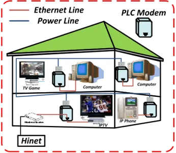
Computer Computer
Power Line
Ethernet Line PLC Modem
TV Game
IP Phone IPTV
Hinet
Fig. 2.1 PLC In-House System
In-house applications are described in a background brief [8]. The application
process occurs with both ends of the communication link in the same building. The building might be a house, an apartment block or an office building. This type of data transmission path in the same building is usually relatively short and usually less than 100 meters between the devices.
Broadband power line communication systems are considered as an attractive means of retrofitting of data services to existing buildings, because it does not require additional wire. For home use and small office systems that it will be very attractive, mainly due to the networking of computers, printers and other telecom services can simply plug into the existing AC power wiring (In principle, the terminal devices used in these systems could potentially be used to link adjacent buildings as well.).
Systems have been successfully developed within short distance applications and can meet the existing electromagnetic compatibility (EMC) requirements of digital information technology (computer) equipment. This is possible due to the relatively short distance within the building (cable) and the required power level is low.
The development of technology for computer networking in-house applications is quite advanced, with industry standard for terminal devices already in place. Interoperable products from different manufacturers also reached (ex. HomePlug). These devices are relatively low cost and easier to use.
Other applications include the use of these systems for sound and video distribution,
and appliance switching and control, within the home. To date, these opportunities have not been developed, or taken up by consumers, to the same degree.
2.3.2 The Challenge of Power Line Communications
Developing an effective implementation of the PLC is not without challenges [11].
There is a lot of noise in power line; you need a reliable infrastructure to maintain the reliability of its data transmission. In addition, each application and operating environment is different, and requires developers to optimize the design and accommodate a variety of factors.
PLC implementations that are too fixed in function can only be applied in a limited number of applications and represent a risky design strategy as standards continue to evolve. Developers need a flexible platform that enables them to optimize designs to the particular requirements of each application and that will allow designs to adapt to new standards and market opportunities as they arise. In this way, intellectual property can be reused across multiple applications to accelerate development and speed time to market while expanding market opportunities.
A key part to achieving flexibility is a modular architecture in terms of hardware and software. Breaking down complex PLC systems into a number of independent subsystems allows developers to change one aspect of a design - such as the modulation
scheme or protocol used - without having to completely redesign the entire system.
2.4 Design Consideration
2.4.1 Power Line Channel Response
The power line shown in Fig. 2.2 is the transmission medium of the power line communication system. There are three common power lines:
Live line: The common colors of the live lines are red and black.
Neutral line: The common color of the neutral line is white.
Ground line: The common color of the ground line is green. But not every building has
the ground lines.
The outlets for the common electrical appliances are using live line and neutral line only. Therefore, the transmission line of the power line communication system in this study is composed of live line and neutral line.
Fig. 2.2 Power Line Fig. 2.3 Power Line with Adapter To measure the channel response, the power line is connected to the SMA adapter
in Fig. 2.3. Moreover, the live line is for signal and the neutral line is for ground. As a result, the 5 meter power line channel response is shown in Fig. 2.4. Furthermore, the equivalent resistance Rpowerline of 5 meter power line with 50 ohm termination in S-parameter measurement is shown in Fig. 2.5. In considering that, the magnitude is changed from tens ohm to hundreds ohm in transmittig frequency band.
Fig. 2.4 Power Line Channel Response
Fig. 2.5 Equivalent RPower Line
2.4.2 EMC Characteristic and Signal Spectrum
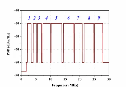
The power spectral density (PSD) mask of the HomePlug AV system divides the 1.8MHz to 28MHz signal bandwidth into 9 sub-bands [12] and the frequency spacing which is used in the MTPR testing of this study is 24.415kHz [13]. The frequency spacing specification of the HomePlug AV is 24.414 kHz.
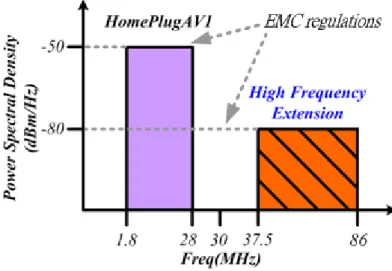
To increase the transmitted data rate of the power line communication system, the bandwidth above 28MHz is used. Moreover, another sub-band from 37.5MHz to 86MHz is defined in HomePlug AV2 specification. However, the output signal PSD of the frequency band which is higher than 28MHz is restricted by electromagnetic compatibility (EMC) consideration [14],[15]. Therefore, the PSD of the high frequency extension band is lower. Moreover, the PSD limitation is shown in Fig. 2.7.
Fig. 2.6 HomePlug AV PSD Mask
Fig. 2.7 HomePlug AV2 EMC Consideration
2.4.3 Line Driver Design Consideration
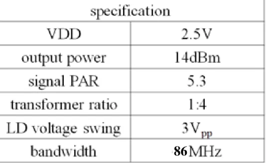
According to the issue described above, it affects line driver design consideration. For the variation of RPower Line, we choose an average value of resistance 50 ohm as the power line model in simulation. It takes lots of power in line driver transmitting signal to a really low equivalent loading on driver output..
On the other hand, power spectral density restriction with two signal bandwidth up to 86MHz and signal peak-to-average power ratio (PAR) are the reasons for the transmitter output power which is needed to deliver 14dBm output power to 50 ohm loading.
As a result, the peak value of voltage onto power line is in 12 to 15 volt range.
Since the chip is fabricated in 90nm process with I/O supply voltage in 2.5 volt, we choose a off-chip step-up transformer with turn ratio 4 and a diffirential amplifier with peak-to-peak output swing 3Vpp to be combined to achive high driving ability. The design specification is shown in Table 2.1.
Table 2-1 Line Driver Design Specification
86
Chapter 3 Analog Front End of Transmitter in PLC system
3.1 Introduction
The analog front end of PLC transmitter is shown in Fig. 3.1, and it consists of a 10-bit current steering digital-to-analog converter (DAC), a low pass filter (LPF) and a line driver. The transmitter output is combined with an off-chip step-up transformer with turns ratio 4 to deliver high output power onto power line in low chip supply voltage and still have good signal linearity. A Sallen-Key filter is used as the low pass filter and to be an interface between DAC and line driver. The Line driver consists a three stage amplifier with a class-AB output stage to drive low output resistance loading.
& LPF
Fig. 3.1 Transmitter Analog Front End
3.2 Sallen-Key Low Pass Filter
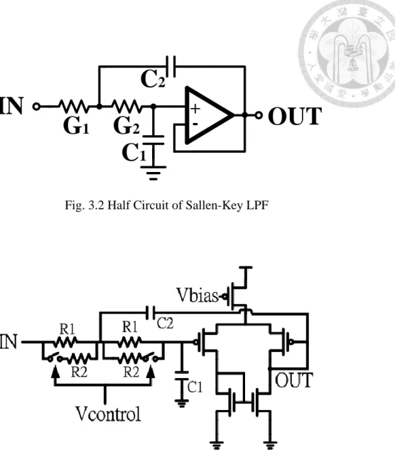
In the integrated PLC transmitter analog front end, the low pass filter is used to reconstruct DAC output signal and filter out unwanted tones in spectrum. In our design, a single stage Sallen-Key low pass filter is chosen and the half circuit is in Fig. 3.2 [16],
[31]. The Sallen-Key low pass filter have been widely used due to their intrinsic design simplicity, wide bandwidth, low noise and very high input impedance. Two conductance 𝐺1, 𝐺2 and two capacitors 𝐶1, 𝐶2 are used to design the parameter of low pass filter
included 𝜔0, Q. The 𝑂𝑈𝑇 𝐼𝑁⁄ transfer function of Sallen-Key low pass filter T(s) is in (3.1)
T(s) =OUT
IN =
𝐺1𝐺2 𝐶2 𝑆2+𝑠[𝐺1+𝐺2]𝐶 +𝐺1𝐺2
𝐶2
= 𝜔02
𝑆2+𝑠𝜔0𝑄 +𝜔02 (3.1) 𝜔0 = √𝐺1𝐺2
𝐶 (3.2) Q = √𝐺1𝐺2
𝐺1+𝐺2 (3.3)
We choose 𝐶1 = 𝐶2 = 𝐶 and 𝐺1 = 𝐺2, then quality factor Q is equal to 1/2. In (3.1) description, we ignore the output resistance ROUT of the unity-feedback amplifier, but it will cause two zeros with 𝜔0𝑍2 = 𝐺2
𝐶1𝐶2𝑅𝑂𝑈𝑇 , and determine high frequency gain.
Furthermore, the stopband rejection will be degraded.
A single stage differential to single end amplifier is used as an unity-feedback buffer shown in Fig. 3.3.
+ -
IN G 1 G 2 OUT C 1
C 2
Fig. 3.2 Half Circuit of Sallen-Key LPF
Fig. 3.3 Low Pass Filter in Active Devices
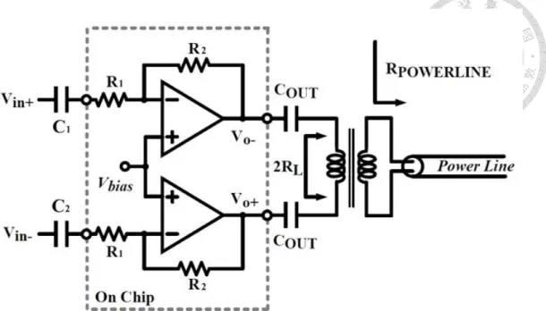
In considering HomePlug AV and AV2 measurements, we design two cut off frequency 100MHz and 50MHz for different bandwidth application. Vcontrol is used for switching resistors to control cut off frequency. The simulation results are shown in Fig. 3.4 and Fig. 3.5.
Fig. 3.4 Low Pass Filter with 100MHz Cut Off Frequency
Fig. 3.5 Low Pass Filter with 50MHz Cut Off Frequency
3.3 PLC Line Driver
The proposed PLC line driver has to drive small resistive output loading.
Furthermore, the loading variation which is caused by the power line channel response makes the PLC line driver design more challenge. The line driver needs to operate up to 86MHz. The details of the proposed line driver are introduced in this chapter.
3.3.1 Closed-Loop Line Driver
The PLC line driver is constructed in pseudo-differential closed-loop amplifier [17], [18] with inverting type resister feedback network in Fig. 3.6. The closed-loop gain is determined by the magnitude ratio of two resisters, R2/R1. Since the high input common mode voltage of line driver, capacitor C1 and C2 are used to isolate output dc voltage from the front stage. Also, Cout is used as output ac coupled capacitor. Input and output common mode voltage are defined by Vbias on non-inverting input. In considering the loading of line driver, the equivalent differential output resistance 2RL from transformer primary side is equal to RPowerLine divided by turn ratio square, 3.125 ohm.
Fig. 3.6 Closed-Loop Line Driver
3.3.2 Half Circuit of Proposed Pseudo-Differential Operational Amplifier
The half circuit of the proposed pseudo-differential operational amplifier is a three-stage amplifier shown in Fig. 3.7.
V
in+V
in-Vb2
V
outC1
Cp Rp
Cn Rn
MF
C2
R1
Vb3
Vb4
Vb1
Vb5 Vb6
MN1
MP1
MN2
Vcp
Vcn MN3 MP2
MOUTP
MOUTN
MAP1 MAP2
Fig. 3.7 Half Circuit of Pseudo-Differential Amplifier
(a) The First and Second Stage
The first stage is a folded cascode differential to single-ended amplifier with PMOS MAP1 and MAP2 to be the input differential pair.
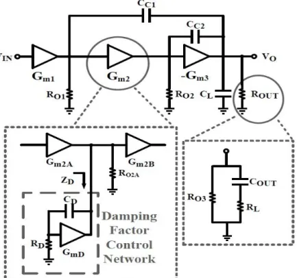
The second stage is a wide band intermediated stage. It is composed of a cascade common source amplifier MP1 and MN2 to deliver high gain and combined with a feed-forward path MF [19] to compensate high frequency band because of the large parasitic capacitance from the output stage in large size. In addition, a damping factor control network [20], MN, R1 and C2, is included to reduce the high frequency peaking.
(b) The Third Stage
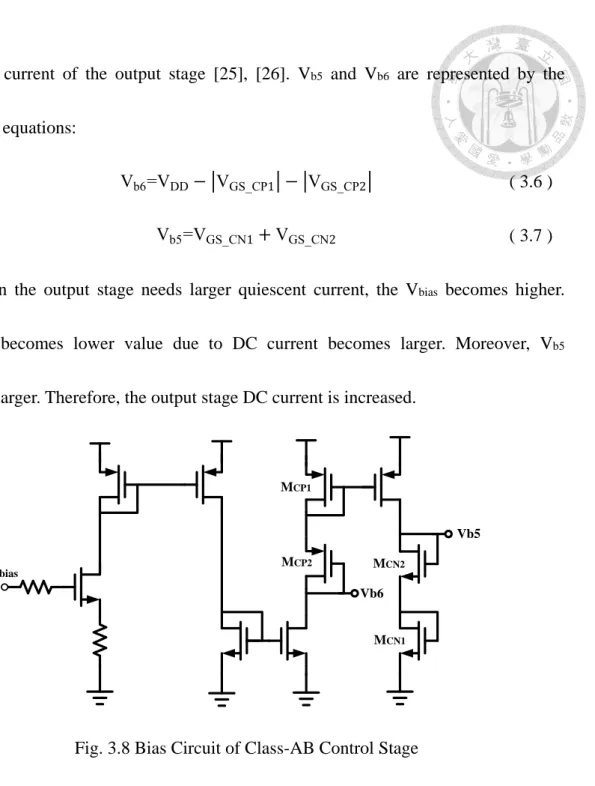
The third stage is a class-AB output stage with proper efficiency and linearity with class AB control circuit [20], [21], [22], [23], [24]. It is used to bias the output stage in class AB operation. Moreover, MN3 and MP2 are the DC voltage level shift. The VCP and
VCN are represented by the following equations:
VCP=Vb6+VSG_P2 ( 3.4 )
VCN=Vb5-VGS_N3 ( 3.5 )
The gate voltage of MOUTP and MOUTN are determined by the Vb5 and Vb6. As a result, the quiescent current of the output stage is controlled by Vb6 and Vb5, too.
The bias circuit for Vb5 and Vb6 of the class AB control stage [21] is shown in Fig.
3.8. Moreover, the class-AB output stage circuit in Fig. 3.7 and Fig. 3.8 determine the
quiescent current of the output stage [25], [26]. Vb5 and Vb6 are represented by the
following equations:
Vb6=VDD− |VGS_CP1| − |VGS_CP2| ( 3.6 )
Vb5=VGS_CN1+ VGS_CN2 ( 3.7 )
When the output stage needs larger quiescent current, the Vbias becomes higher.
The Vb6 becomes lower value due to DC current becomes larger. Moreover, Vb5
becomes larger. Therefore, the output stage DC current is increased.
Vb5
Vb6 MCP1
MCP2
MCN1
MCN2
Vbias
Fig. 3.8 Bias Circuit of Class-AB Control Stage (c) Frequency Compensation
For three-stage amplifier stability issue, nested Miller compensation (NMC) [5] is used to increase phase margin. The capacitor CC1 is the main compensation capacitor which determines the dominant pole. Furthermore, CP, RP, CN, and RN are used to determined non-dominate pole and confirm enough phase margin.
3.3.3 Damping Factor Control Network
The nested Miller compensation (NMC) multi-stage amplifier with damping factor control network model is shown in Fig 3.9. In the NMC amplifier, two capacitors CC1
and CC2 are applied for frequency compensation. For broadband PLC system, CC2
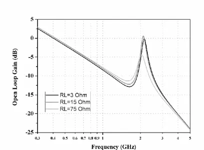
should be smaller to broaden the bandwidth [4], [27] but it makes damping factor uncontrollable.
Three-stage amplifier with nested Miller compensation has better linearity than two stage with Miller compensation, but the damping factor is an important issue. When damping factor is low, there is a peaking occurred in transfer function. However, as shown in Fig. 2.5, the measured equivalent resistance RPOWER LINE of power line changes severely from tens ohm to thousands ohm independent with the frequency. Considering to the simulation results as shown in Fig. 3.9, we apply three different output equivalent resistances in simulation. The high frequency peaking points cross 0dB line and lead the circuit to be unstable. Consequently, high frequency peaking effect should be suppressed. In this work, a damping factor control (DFC) network including RD, CD and GmD [25], is adopted to maintain a high damping factor for stability issue. The simulation results of the proposed pseudo-differential op amp with DFC network are shown in Fig. 3.10.
When frequency is larger than unity gain bandwidth of the open-loop transfer
function, the damping factor 𝜁 of open-loop transfer function will be lower than the
value in signal bandwidth and it is written in (3.5) 𝜁 =1
2×𝐶𝐶2 (𝐺𝑚3−𝐺𝑚2)
√𝐺𝑚2𝐺𝑚3𝐶𝐿𝐶𝐶2 (3.8) and 𝐺𝑚2 = 𝐺𝑚2𝐴𝐺𝑚2𝐵(𝑍𝐷//𝑅𝑂2𝐴) (3.9) and 𝑍𝐷 = 1+𝑆𝐶𝐷𝑅𝐷
𝑆𝐶𝐷(1+𝐺𝑚𝐷𝑅𝐷) (3.10)
In high frequency, ZD can be approach to 1/GmD which becomes smaller. Therefore, as the frequency increasing, Gm2 will be decreasing. As a result, the damping factor will remain large value that the high frequency peaking effect will be suppressed. Finally, the stability will be improved while equivalent resistance RPOWERLINE varies in PLC system.
Fig. 3.9 Multi-Stage Amplifier Model with DFC
Fig 3.10 Peaking Effects with Load Variation
Fig 3.11 Peaking Reduction with DFC
3.3.4 Distortion Consideration in NMC Amplifier
In the reference paper [28], [29], [30] description, distortion in frequency domain due to weakly nonlinear sources is analyzed to estimate open-loop and closed-loop linearity. Nonlinear voltage gain of each stage is expressed in 𝐴𝑁𝐿 𝐼 , 𝐴𝑁𝐿𝐼𝐼 , 𝑎𝑛𝑑 𝐴𝐼𝐼𝐼𝑁𝐿, and they consist of power series with different distortion coefficients. Miller capacitances 𝐶𝐶1 and 𝐶𝐶2 are form the local feedback loop and the diagram will be transformed
from NMC compensation structure to the diagram in Fig. 3. . In the equivalent network, 𝜔𝐶1 and 𝜔𝐶2 are represent two poles include 𝐶𝐶1 with resistance connected to first
stage and 𝐶𝐶2 with resistance connected to second stage. When input 𝑣𝑑 is defined as 𝑉𝑑ejωt, the output 𝑣𝑜 will be 𝑎1(𝑗𝜔)𝑉𝑑ejωt + 𝑎2(𝑗𝜔)𝑉𝑑2ej2ωt + 𝑎3(𝑗𝜔)𝑉𝑑3𝑒−𝑗3𝜔𝑡 . To further simplify the nested loop from inner one, we need to let the loop to be open and transform the loop to an open nonlinear stage and combine two nonlinear stages into a new one [30].
Fig. 3.12 Nonlinear Diagram of Three-Stage NMC Amplifier
Using the NMC amplifier mentioned above in the inverting closed-loop configuration as the line driver structure in this topic, it has a better linearity performance than the non-inverting type. The closed-loop amplifier is shown in Fig.
3.13 with α = 𝑅2
(𝑅1+𝑅2) and β = 𝑅1
(𝑅1+𝑅2) . The third harmonic distortion coefficient H3 of the output Vo is the black dash line shown in Fig. 3.14.
Fig. 3.13 Inverting Closed-Loop Configuration
The third order distortion will be eliminated by being divided by loop gain𝐴1𝐴2𝐴3𝛽 [28], but it will increase by using higher resistor ratio for high loop gain.
𝐴1𝐴2𝐴3 is a linear gain of three-stage. However, the most contribution in the third
order harmonic distortion is output stage. The performance will decay when frequency higher than the poles inside the amplifier included dominate and non-dominate poles.
Considering only the third harmonic distortion of output stage, in contrast with one-stage and two-stage, three-stage amplifier has better performance below 100MHz in Fig. 3.15. Since non-linearity of line driver output stage is from cross over distortion and large size for current driving, it is usually dominate distortion performance. In our line driver design, we use the consideration above to design three-stage amplifier in
driver and parameter for Miller compensation.
Fig. 3.14 Third Harmonic of Different Amplifier
Fig. 3.15 Third Harmonic about Output Stage in Different Amplifier
3.3.5 Open-Loop AC Simulation
The DC power in open-loop ac simulation is 515.2320mW for half pseudo-differential at SS/100°𝐶 and 618.5799mW for TT/40°𝐶 . Furthermore, the open-loop frequency response simulation results of the multi-stage amplifier and transformer with turn ratio 4 are shown in Fig. 3.16 and Fig. 3.17. The differential equivalent loading is 3.125 ohm. Moreover, the open-loop DC gain at SS/100°𝐶 is about 102dB, the unity gain frequency is about 321MHz, and the phase margin is 75°. The open-loop DC gain at TT/40° is about 100dB, the unity gain frequency is about 453MHz, and the phase margin is 79°
Fig. 3.16 Open-Loop Transfer Function at SS/100°𝐶
Fig. 3.17 Open-Loop Transfer Function at TT/40°𝐶
3.3.6 Closed-Loop AC Simulation
The closed-loop line driver gain of resistor ratio is chosen to be 6.33. Furthermore, the input and output common mode voltages are all defined to 1.25V. The simulation results of the proposed pseudo-differential closed-loop line driver and transformer with turn ratio 4 are shown. The closed-loop gain is 16 dB and the -3dB bandwidth is 71.6MHz for SS/100°𝐶 shown in Fig. 3.18. Furthermore, the closed-loop gain is 16 dB and the -3dB bandwidth is 74.7MHz for TT/40°𝐶 shown in Fig. 3.19
Fig. 3.18 Closed-Loop Transfer Function at SS/100°𝐶
Fig. 3.19 Closed-Loop Transfer Function at TT/40°𝐶
3.3.7 Transient Simulation Result of Closed-Loop Line Driver
The transient simulation results of closed-loop line driver and transformer with turn ratio 4 is shown. The closed loop gain is 6.33 and the input signal is 500mv peak-to-peak. The differential equivalent resistance loading is 3.125 ohm.
Fig. 3.20 shows the FFT result for 30 MHz input frequency at SS/100°𝐶 and HD3
is 62dB. Fig. 3.21 shows the FFT result for 80 MHz input frequency at SS/100°𝐶 and HD3 is about 40dB.
Fig. 3.22 shows the FFT result for 30 MHz input frequency at TT/40°𝐶 and HD3 is about 70dB. Fig. 3.23 shows the FFT result for 80 MHz input frequency at TT/40°𝐶 and HD3 is about 40dB.
Fig. 3.20 FFT Result for 30MHz Input at SS/100°𝐶
Fig. 3.21 FFT Result for 80MHz Input at SS/100°𝐶
Fig. 3.22 FFT Result for 30MHz Input at TT/40°𝐶
Fig. 3.23 FFT Result for 80MHz Input at TT/40°𝐶
3.4 Transmitter Simulation
The co-simulation FFT result of DAC and analog front end is shown in Fig. 3.24.
The input digital codes for DAC are generated by Matlab and the input frequency is 99.8 MHZ. The sampling clock of DAC is 200 MHz decided by Nyquist rate theorem from PLL inside the chip. The overall SNR of transmitter output achieves 53.6 db in simulation. The SNR result is higher than 36 db.
Fig. 3.24 SNR of Transmitter Output
Chapter 4 Transmitter Measurement
4.1 PLC Chip Photo and Transmitter Amplifier Layout
The integrated PLC transceiver is fabricated in TSMC 90nm 1.2/2.5V process. The whole chip photo is shown in Fig. 4.1 and the chip size is 2.63 x 2.52 mm2 including pads. The layout of line driver in transmitter amplifier is in Fig. 4.2 and the active area is 1000 μm x 700 μm .
Fig. 4.1 PLC chip photo
Fig. 4.2 Line Driver layout
4.2 Measurement Environment Setting
Transmitted signal in PLC output is modulated in QAM, such as 512 QAM or 1024 QAM. The measurement plan is shown in Fig. 4.3. In order to create input codes to DAC, we encode QAM signal by Matlab and realize digital codes by pattern generator Tektronix TLA715. The output signal of line driver is pass through transformer coupler shown in Fig. 4.4 with turn ration 1:4 and measured by spectrum analyzer Agilent N9030A PXA for distortion and MTPR testing.
The received signal is also passed through transformer with turn ratio 4:1 to receiver and the output of receiver is measured by logic analyzer TLA5203 for loopback MTPR and recovered QAM measurement.
There are two interconnected lines include SMA cable and power line used
between transmitter and receiver for loopback measurement shown in Fig. 4.5. In the following results, we choose SMA cable as the channel because we want to ignore the complicated channel response and observe only transmitter output response to figure out where the problem is.
Matlab
DAC
ADC
Fig. 4.3 Measurement Environment Setting
Fig. 4.4 Coupler Fig. 4.5 Power Line in Measurement
4.3 MTPR and Recovered QAM Measurement
The following measurement results are classified in HomePlug AV and AV2
specifications. In each case, there are transmitting signal MTPR, received signal MTPR and recovered QAM.
4.3.1 HomePlug AV Specification Measurement
Fig. 4.6 Transmitter Output MTPR for HomePlug AV
Fig. 4.7 Loopback MTPR for HomePlug AV
Fig. 4.8 Recovered QAM for HomePlug AV
4.3.2 HomePlug AV2 Specification Measurement
Fig. 4.9 Transmitter Output MTPR for HomePlug AV2
Fig. 4.10 Loopback MTPR for HomePlug AV2
Fig. 4.11 Recovered QAM for HomePlug AV2
4.3.3 Performance Summary
The transceiver measurement results summary table is in Table 4.1. For HomePlug AV2 bandwidth application, the power consumption is 1.1 W. The MTPR performance for HomePlug AV1 is larger than 40dB and larger than 36dB for HomePlug AV2. The transmitter amplifier are all bias in 2.5 V for VDD with I/O devices used.
Table 4-1 Transceiver Measurement Summary
Chapter 5 Conclusion
By using nested Miller compensation and feed forward path compensation, the wideband and more linear line driver can be achieved. The damping factor control network is the solution for frequency peak at frequency higher than unity gain bandwidth in open-loop transfer function. The Sallen-Key low pass filter and the line driver with the characteristic mentioned before are simulated and fabricated in TSMC 90nm process.
In order to achieve better distortion performance, we should do some improvement on line driver. First of all, a floating capacitor needed to be put parallel to level shifter for class-AB control circuit. It creates a high frequency path to the gate of PMOS in output stage to equalize to NMOS path in transfer function and stabilize the voltage difference between Vcp and Vcn from cross over distortion in output stage. Then we can put another path like MN2 to Vcp to achieve another fast path to improve linearity of
output stage and equalize two paths.
Common mode feedback circuit is needed to add in pseudo-differential amplifier to stabilize the bias of output stage and it improves the common mode transfer function of line driver.
Reference
[1] HomePlug Alliance official website: http://www.homeplug.org/
[2] “HomePlug AV white paper,” HomePlug Powerline Alliance, 2005.
[3] 劉邦楷, “A Line Driver Design for Powerline Communication Systems,” Master Thesis, NTU, 2012.
[4] K. N. Leung, P. K. T. Mok, W. H. Ki, and J. K. O. Sin, “Three-stage large capacitive load amplifier with damping-factor-control frequency compensation,”
IEEE J. Solid-State Circuits, vol. 35, no. 2, pp. 221-230, Feb. 2000.
[5] K. N. Leung and P. K. T. Mok, “Analysis of multistage amplifier-frequency compensation,” IEEE Trans. Circuits Syst. I, vol. 48, no. 9, pp. 1041-1056, Sept.
2001.
[6] K. N. Leung and P. K. T. Mok, “Nested Miller compensation in low-power CMOS design,” IEEE Trans. Circuits Syst. II, vol. 48, no. 4, pp. 388-394, April 2001.
[7] 詹凱翔, “A High Dynamic Range, Low Gain Error Programmable Gain Amplifier for Powerline Communication System,” Master Thesis, NTU, 2012.
[8] Spectrum Planning Team, Radiofrequency Planning Group, Australian Communications Authority, Broadband Powerline Communications Systems: A
Background Brief, Sep. 2003. Retrieved from:
https://docs.google.com/viewer?url=http://www.acma.gov.au/webwr/radcomm/fre
quency_planning/spps/0311spp.pdf&pli=1
[9] Halid Hrasnica, Abdelfatteh Haidine, and Ralf Lehnert, Broadband Powerline Communications Networks: Network Design, England, John Wiley & Sons Ltd,
2004.
[10] HomePlug. (n.d.). Retrieved March 19, 2012, from http://en.wikipedia.org/wiki/HomePlug
[11] Olivier Monnier, “TI Delivers Flexible Power Line communications Solutions,”
White Paper, Texas Instruments, 2010.
[12] “HomePlug AV specification version 1.1,” HomePlug Powerline Alliance, May 2007.
[13] N. Weling, “Expedient permanent PSD reduction table as mitigation method to protect radio services,” IEEE International Symposium on Power Line
Communications and Its Applications (ISPLC), pp. 305-310, April 2011.
[14] K. Findlater, T. Bailey, A. Bofill, N. Calder, S. Danesh, R. Henderson, W. Holland, J. Hurwitz, S. Maughan, A. Sutherland, and E. Watt, “A 90nm CMOS
dual-channel powerline communication AFE for Homeplug AV with a Gb extension,” IEEE ISSCC Dig. Tech. Papers, pp. 464-628, Feb. 2008.
[15] M. Tlich, R. Razafferson, G. Avril, and A. Zeddam, “Outline about the EMC properties and throughputs of the PLC systems up to 100 MHz,” IEEE
International Symposium on Power Line Communications and Its Applications
(ISPLC), pp. 259-262, April 2008
[16] R. Schaumann, M. E. V. Valkenburg, and H. Xiao, Analog Filter Design, 2nd edition Oxford University Press, 2011
[17] A. N. Mohieldin, E. Sanchez-Sinencio, and J. Silva-Martinez, “A fully balanced pseudo-differential OTA with common-mode feedforward and inherent common-mode feedback detector,” IEEE J. Solid-State Circuits, vol. 38, no. 4, pp.
663-668, April 2003.
[18] C. Lujan-Martinez, R. G. Carvajal, J. Galan, A. Torralba, J. Ramirez-Angulo, and A. Lopez-Martin, “A tunable pseudo-differential OTA with -78 dB THD consuming 1.25 mW,” IEEE Trans. Circuits Syst. II, Exp. Briefs, vol. 55, no. 6, pp.
527-531, June 2008.
[19] M. S. Kappes, “A 3-V CMOS low-distortion class AB line driver suitable for HDSL applications,” IEEE J. Solid-State Circuits, vol. 35, no. 3, pp. 371-376,
March 2000.
[20] V. Dhanasekaran, J. Silva-Martinez, and E. Sanchez-Sinencio, “Design of three-stage class-AB 16 Ω headphone driver capable of handling wide range of load capacitance, ” IEEE J. Solid-State Circuits, vol. 44, no. 6, pp. 1734-1744, June 2009.
[21] D. M. Monticelli, “A quad CMOS single-supply op amp with rail-to-rail output swing,” IEEE J. Solid-State Circuits, vol. SC-21, no. 6, pp. 1026-1034, Dec. 1986.
[22] Xicheng Jiang, Jungwoo Song, T. L. Brooks, Jianlong Chen, V. Chandrasekar, F.
Cheung, S. Galal, D. Cheung, G. C. Ahn and M. Bonu, “A 10mW stereo audio CODEC in 0.13μm CMOS,” IEEE ISSCC Dig. Tech. Papers, pp. 82-83, Feb.
2010.
[23] G. Cesura, A. Bosi, F. Rezzi, R. Castello, Jenkin Chan, SaiBun Wong, Chi Fan
Yung, O. Carnu, and T. Cho, “A VDSL2 CPE AFE in 0.15μm CMOS with integrated line driver,” IEEE ISSCC Dig. Tech. Papers, pp. 108-109,109a, Feb.
2009.
[24] M. S. Kappes, “A 3-V CMOS low-distortion class AB line driver suitable for HDSL applications,” IEEE J. Solid-State Circuits, vol. 35, no. 3, pp. 371-376,
March 2000.
[25] E. Seevinck, and R. J. Wiegerink, “Generalized translinear circuit principle,”
IEEE J. Solid-State Circuits, vol. 26, no. 8, pp. 1098-1102, Aug. 1991.
[26] B. A. Minch, “MOS translinear principle for all inversion levels,” IEEE Trans.
Circuits Syst. II, Exp. Briefs, vol. 55, no. 2, pp. 121-125, Feb. 2008.
[27] P. K. Liu, S. Y. Hung, C. Y. Liu, M. H. Hsieh, and C. C. P. Chen, “A 52 dBc MTPR line driver for powerline communication HomePlug AV standard in
0.18-μm CMOS technology,” in Proc. IEEE Int. Symp. Circuits Systems, May.
2013, pp. 1404–1407.
[28] B. Hernes and W. Sansen, “Distortion in single-, two- and three-stage amplifiers,”
IEEE Trans. Circuits Syst. I, Fundam. Theory Appl., vol. 52, no. 5, pp. 846–856,
May 2005.
[29] G. Palumbo and S. Pennisi, “Harmonic distortion in three-stage nested-Miller-compensated amplifiers,” in Proc. IEEE Int. Symp. Circuits Systems, May. 2004, pp. 485–488.
[30] S. O. Cannizzaro, G. Palumbo, and S. Pennisi, “Distortion analysis of Miller-compensated three-stage amplifiers,” IEEE Trans. Circuits Syst. I, Reg.
Papers, vol. 53, no. 5, pp. 961–976, May 2006.
[31] F. Resta1, M. De Matteis1, A. Pezzotta1, S. D’Amico2, and A. Baschirotto, “A 30MHz 28dBm-IIP3 3.2mW Fully-Differential Sallen-Key 4th-Order Filter with Out-of-Band Zeros Cancellation,” in Proc. IEEE Int. New Circuits Syst. Conf., Jun.
2015.