國立臺灣大學電機資訊學院電子工程學研究所 碩士論文
Graduate Institute of Electronics Engineering College of Electrical Engineering & Computer Science
National Taiwan University Master Thesis
六方氮化硼基板應用於二硫化鉬薄膜電晶體 與二硫化鉬-黑磷異質接面特性探討
Study of MoS
2TFT with Hexagonal Boron Nitride Substrate and MoS
2-Black Phosphorus Heterostructures
洪彬超 Pin-Chao Hung
指導教授:李嗣涔 博士 Advisor: Lee Si-Chen, Ph.D.
中華民國 107 年 7 月
July, 2018
中文口試委員審定書
致謝
在碩士班這兩年能夠順利的完成論文並且畢業,首先要感謝我的指導教授李
嗣涔博士,感謝老師給我研究上的指導,讓我找到研究方向。接著感謝2D 組的學
長張簡、昌哥、博彥,帶領我進入二維材料的領域,並且教導我如何使用儀器及實 驗技巧。另外,也要感謝吳志毅老師實驗室的黃國祐學長、李家碩學長、沈新偉學 長及吳肇欣老師實驗室的范鎧麟同學,在實驗上給予我協助。
接著,感謝實驗室的助理馬姐,幫我們處理實驗室許多大大小小的事務,讓我 能夠專心地在研究上。感謝實驗室的黃偉倫學長、湯明儒學長、洪宗宏學長,不論 是操作機台或是各項事務上也都給了我很大的幫助。也感謝與我同屆的實驗室成 員曾奕融、蕭堯,有了你們的陪伴讓我在實驗上不會感到枯燥。也祝福學弟妹們:
余凱文、彭天欣、王奇樺、郭哲劭實驗順利,準時畢業。
最後要感謝我的爸媽,有了你們的支持,讓我在求學期間沒有後顧之憂,並順 利完成碩士學位,謝謝你們。謹以此論文獻給你們。
摘要
本論文使用機械剝離法分離出擁有奈米級厚度的二硫化鉬並利用二氧化矽基 板製作出薄膜電晶體,利用光學顯微鏡及原子力顯微鏡的搭配篩選出較佳厚度範 圍的二硫化鉬,並利用低功函數金屬鉻當作金屬電極來達成歐姆接觸。其電晶體最
好的場效電子遷移率可以達到 44.7 cm2/V-s 與最低遲滯為 46.2 V。相較於二氧化
矽,六方氮化硼具有較平滑的表面且無懸浮鍵與電荷缺陷,故以其取代二氧化矽作 為二硫化鉬薄膜電晶體的基板以改善場效電子遷移率與降低遲滯效應。藉由導入
六方氮化硼基板,二硫化鉬薄膜電晶體的場效電子遷移率能提升至 117 cm2/V-s,
遲滯降低至5 V。此外,藉由比較二硫化鉬薄膜電晶體在兩種不同基板且不同大氣
環境下,顯示遲滯效應主要是由二硫化鉬與氧化層之間接面特性所影響,而吸附在 二硫化鉬表面的水氣與氧氣並不會造成遲滯效應。然而吸附在表面的水氣與氧氣 會使二硫化鉬薄膜電晶體的特性隨時間而下降,因此六方氮化硼被用來當作二硫 化鉬薄膜電晶體的保護層並且能使其有更好的穩定度。
接著使用三氟甲烷電漿使二硫化鉬薄膜有p 型電洞參雜,且藉由 X 光光電子
能譜儀可得知參雜後其費米能階往價電帶下降 0.4 eV。因此藉由三氟甲烷電漿參
雜二硫化鉬形成p 區並結合未參雜的二硫化鉬(n 區)成功的製作出二硫化鉬整流二
極體,其開關電流比值大約為100 倍、理想因子為 2.44。然而為了有更好的理想因
子(介於 1 與 2 之間),p 型二維材料黑磷被用來取代三氟甲烷電漿參雜的二硫化鉬
並與未參雜二硫化鉬結合製作出二硫化鉬-黑磷異質接面,其開關電流比值大約為 30 倍、理想因子為 1.84。最後利用寬頻氙燈量測二硫化鉬整流二極體與二硫化鉬- 黑磷異質接面的光學特性,可以發現雖然二硫化鉬-黑磷異質接面的光響應比二硫 化鉬整流二極體還要小,但二硫化鉬-黑磷異質接面有著比二硫化鉬整流二極體還 要好的光偵測能力。
關鍵字:二硫化鉬薄膜二極體、六方氮化硼、遲滯效應、p 型電洞參雜、二硫化鉬 -黑磷異質接面
ABSTRACT
In this thesis, the mechanically exfoliated 2D material MoS2 nanosheet was successfully used to fabricate thin film transistor (TFT) on SiO2 substrate. By using optical microscopy and atomic force microscopy, the MoS2 flakes with appropriate thickness can be chosen. Ohmic contact of MoS2 TFT can be achieved by low work function metal Chromium. The highest mobility of MoS2 TFT on SiO2 substrate is 44.7 cm2/V-s and the lowest hysteresis is 46.2 V. In order to further improve the mobility and reduce the hysteresis, the SiO2 substrate was replaced by h-BN substrate because h-BN has an atomically smooth surface that is relatively free of dangling bonds, charge traps and is naturally flat which can improve the interface property between MoS2 and oxide layer. By introducing h-BN substrate, the mobility of MoS2 TFT can be improved to 117 cm2/V-s and its hysteresis can be reduced to 5 V. Furthermore, by comparing the performance of MoS2 TFTs among SiO2 and h-BN substrates with different atmospheric environment, it shows that interface property between MoS2 and oxide layer would influence hysteresis seriously and the molecules such as H2O and O2 adsorbed on MoS2
surface would not cause hysteresis. However, the molecules such as H2O and O2 adsorbed on MoS2 surface would degrade the characteristics of MoS2 TFT. Therefore, the h-BN passivation layer is used to passivated the MoS2 TFT and it shows it has better stability
by using h-BN passivation layer.
Besides, the CHF3 plasma was used to dope the MoS2 film to p-type material. By using XPS analysis, it shows that the Fermi level of MoS2 film would shift about 0.4 eV toward the valence band. Therefore, CHF3 plasma doping is used to generate p-region and combine with pristine MoS2 (n-region) to fabricate MoS2 rectifying diode. The current rectification ratio is about 2 order and its ideality factor is 2.44. In order to have better ideality factor (in the interval between 1 and 2), black phosphorus(BP) which is p- type 2D material is used to combine with MoS2 to fabricate MoS2-BP heterostructure n- p junction. The current rectification ratio is 30 and its ideality factor is 1.84 which is better than MoS2 rectifying diode. Finally, the Xe lamp which is broadband light source is used to measure optical properties of MoS2 rectifying diode and MoS2-BP heterostructure n-p junction. It shows that although MoS2-BP heterostructure n-p junction has lower responsivity than MoS2 rectifying diode, it has better photodetecting ability than MoS2
rectifying diode.
Key words: molybdenum disulfide (MoS2) thin film transistor (TFT), hexagonal boron nitride (h-BN), hysteresis effect, p-type doping, MoS2-Black Phosphorus heterostructure
CONTENTS
中文口試委員審定書 ... i
致謝 ... ii
摘要 ... iii
ABSTRACT ... v
CONTENTS ... vii
LIST OF FIGURES ... xi
LIST OF TABLE... xvii
Chpater 1 Introduction ... 1
1.1 Overview of Molybdenum Disulfide ... 1
1.2 Advantages of MoS2 FETs ... 8
1.3 Motivation ... 11
Chpater 2 Experiments ... 14
2.1 Heterostructure Fabrication System ... 14
2.2 Reactive Ion Etching System ... 17
2.3 Measurement Techniques ... 18
2.3.1 Atomic Force Microscopy (AFM) ... 18
2.3.2 Raman Spectroscopy ... 18
2.3.3 Photoluminescence (PL) ... 19
2.3.4 Photoemission Spectroscopy (PES) ... 20
2.3.5 Current-Voltage Characteristics ... 22
2.4 Rapid Thermal Annealing (RTA) ... 23
Chpater 3 Material Analysis ... 24
3.1 Substrate Preparation ... 24
3.2 Preparation of Exfoliated MoS2 ... 26
3.3 Characterization of MoS2 Film Thickness ... 26
3.3.1 Optical Microscopy ... 27
3.3.2 Atomic Force Microscopy(AFM) ... 28
3.4 Optical and Vibrational Properties of MoS2 ... 31
3.4.1 Raman Spectroscopy ... 31
3.4.2 Photoluminescence(PL) ... 33
3.5 X-ray Photoelectron Spectroscopy(XPS) ... 37
3.5.1 XPS spectrum of MoS2 ... 38
3.5.2 Stability of MoS2 in Air ... 39
3.5.3 Material Analysis of RIE doped MoS2 ... 41
3.6 Ultraviolet photoelectron spectroscopy(UPS) ... 43
3.6.1 Work Function of MoS2 ... 45
3.6.2 Material Analysis of RIE doped MoS2 ... 47
Chpater 4 MoS2 Thin Film Transistors ... 49
4.1 MoS2 Back-gated TFTs using SiO2 Substrate ... 49
4.1.1 Device Process Flow ... 49
4.1.2 Device Performance ... 52
4.2 MoS2 Back-gated TFTs using h-BN Substrate ... 56
4.2.1 Device Process Flow ... 56
4.2.2 Device Performance ... 59
4.3 Comparison between SiO2 and h-BN Substrate ... 62
4.3.1 Device Process Flow ... 62
4.3.2 Device Performance ... 64
4.4 Discussion of hysteresis and stability of MoS2 TFT ... 67
4.4.1 Hysteresis in MoS2 back-gated TFTs ... 67
4.4.2 Stability in MoS2 back-gated TFTs... 69
4.5 MoS2 p-n rectifying diode ... 71
4.5.1 Device Process Flow ... 71
4.5.2 Device Performance ... 73
4.6 MoS2-Black phosphorus (BP) heterostructure ... 78
4.6.1 Device Process Flow ... 78
4.6.2 Device Performance ... 80
4.7 Summary ... 87
Chpater 5 Conclusions ... 88
References ... 90
LIST OF FIGURES
Fig. 1.1 The transition metals and the three chalcogen elements are shown in the periodic
table ... 3
Fig. 1.2 Three dimensional representation of the structure of MoS2 ... 3
Fig. 1.3 Three polytypes of MoS2: 2H (two layers per unit cell), 3R (three layers per unit cell) and 1T (one layer per unit cell). ... 4
Fig. 1.4 The metal coordination and top view of 1T, 2H, and 3R phase. ... 4
Fig. 1.5 Calculated band structures of (a) bulk (b) quadrilayer (c) bilayer, and (d) monolayer MoS2. ... 6
Fig. 1.6 Band gap energy of MoS2 as function of layer number for N= 1~6. ... 6
Fig. 1.7 (a) A simple planar structure of FET. (b)The potential ( )x distribution from the source to drain. (c) The potential energy distribution U x( ) for electrons from the source to drain. ... 10
Fig. 2.1 Three axis micrometer stage. ... 15
Fig. 2.2 Heterosutructure fabrication system. ... 15
Fig. 2.3 PDMS Stamp. ... 16
Fig. 2.4 h-BN flake on SiO2/Si substrate under optical microscope. ... 16
Fig. 2.5 MoS2 flake on PDMS under optical microscope. ... 16
Fig. 2.6 Heterostructure of MoS2 and hBN ... 17
Fig. 2.7 Diagram of RIE setup ... 18
Fig. 2.8 Diagram of how photoelectron is generated. ... 20
Fig. 2.9 The band diagram of an unknown material. ... 21
Fig. 3.1(a) Thickness dependence of color and (b) contrast in optical microscope. ... 25
Fig. 3.2 Exfoliated MoS2 on 300nm SiO2/Si substrate under optical microscopy ... 28
Fig. 3.3(a) OM image of exfoliated MoS2. AFM line profile for (b) blue (c) green (d) yellow (e) orange color of MoS2 film. ... 30
Fig. 3.4 Schematic illustration of in-plane phonon modes E12g and the out-of-plane phonon mode A1g for MoS2. ... 32
Fig. 3.5 Thickness dependent Raman spectra for MoS2. ... 33
Fig. 3.6 Calculated band structures of (a) bulk (b) quadrilayer (c) bilayer, ... 34
Fig. 3.7 Photoluminescence spectra for monolayer, 4-layer and bulk MoS2. ... 35
Fig. 3.8 The band structure of monolayer MoS2 with the label of C calculated by the DFT. The arrows indicate the transition in A, B and the band nesting. ... 36
Fig. 3.9 The band diagram of X-ray photoelectron spectroscopy... 38
Fig. 3.10 X-ray photoelectron spectroscopy for (a) Mo (b) S ... 39 Fig. 3.11 (a) Raman Spectra for monolayer and bulk MoS2,respectively. (b) XPS profile
of the oxygen intensity at surface and inner MoS2. ... 40
Fig. 3.12 The XPS spectra for (a) Mo 3d (b) F 1s (c) O 1s binding energy before and after plasma treatment. (d) The reported[73] XPS for Mo binding energy in the MoS2 and MoO3. ... 42
Fig. 3.13 Band diagram of an unknown material. ... 44
Fig. 3.14 (a), (b) and (c) UPS spectra of pristine MoS2 ... 46
Fig. 3.15 Band diagram of bulk MoS2 ... 46
Fig. 3.16 UPS spectra for (a) 30s (b) 60s plasma treatment ... 48
Fig. 3.17 The band diagram of (a) pristine (b) plasma treatment for 30s (c) plasma treatment for 60s MoS2. ... 48
Fig. 4.1 Patterned Substrate ... 50
Fig. 4.2 The flow chart for back-gated MoS2 TFT fabrication process. ... 51
Fig. 4.3 (a) Cross-section view of device structure. (b) Top view of MoS2 TFT under optical microscopy. ... 51
Fig. 4.4 (a) top view of MoS2 TFT under AFM. (b) The thickness of the MoS2 flake measured by AFM. ... 53
Fig. 4.5 The characteristics of SiO2 substrate MoS2 TFT (a) Id versus Vd characteristics. (b) Id versus Vg curves in log and linear scale. ... 54
Fig. 4.6 The flow chart for MoS2 back-gated TFT using h-BN substrate. ... 56
Fig. 4.7 Schematic flow of the fabrication process of h-BN substrate TFT. ... 57
Fig. 4.8 Top view of h-BN substrate TFT under optical microscopy. ... 58
Fig. 4.9 Raman spectra of h-BN substrate MoS2 TFT. ... 58
Fig. 4.10 The characteristics of h-BN substrate MoS2 TFT (a) Id versus Vd (b) Id versus Vg curves in log and linear scale. ... 60
Fig. 4.11 AFM image for the thickness of h-BN. ... 61
Fig. 4.12 MoS2 and h-BN heterostructure with (a) The whole MoS2 flake on the h-BN (b) half of MoS2 flake on the h-BN under optical microscopy. ... 63
Fig. 4.13 (a)Cross-sectional view of device structure. (b) Top view of MoS2 TFT under optical microscopy. Electrodes 1 and 2 are the TFT on SiO2 substrate, whereas electrodes 3 and 4 are the TFT on h-BN substrate. ... 63
Fig. 4.14 Id versus Vd characteristics of TFTs on the (a) SiO2 substrate (b) h-BN substrate. They use the same MoS2 flake. ... 64
Fig. 4.15 AFM image for the thickness of h-BN. ... 65
Fig. 4.16 Id versus Vg characteristics of TFTs on the (a) SiO2 substrate (b) h-BN substrate. They use the same MoS2 flake. ... 66 Fig. 4.17 Hysteresis in transfer characteristics of MoS2 TFT on SiO2 substrate (a) before
and after annealing (b) after annealing but measure in atmosphere and vacuum(~0.1 torr).
... 68 Fig. 4.18 MoS2 back-gated TFT (a) without (b) with h-BN passivation layer. ... 69 Fig. 4.19 The variety of (a) mobility (b) on/off ratio (c) subthreshold swing after MoS2
TFTs exposure in air for 28 days. ... 70 Fig. 4.20 The flow chart for MoS2 p-n rectifying diode fabrication process. ... 71 Fig. 4.21 Schematic flow of the fabrication process of MoS2 rectify diode... 72 Fig. 4.22 (a) MoS2 flake with half region open(inside the dashed line) (b) Top view of MoS2 rectifying diode under optical microscopy. ... 73 Fig. 4.23 Id versus Vd of MoS2 rectifying diode in log scale. ... 74 Fig. 4.24 The emission spectra of Xe lamp. ... 74 Fig. 4.25 The photoresponse of MoS2 rectifying diode with different light intensity illumination. ... 76 Fig. 4.26 Id versus Vd characteristics of MoS2 rectifying diode under various incident light intensity. The inset shows the details in the reverse bias region. ... 77 Fig. 4.27 Photodetection responsivity of MoS2 rectifying diode versus incident light intensity. ... 77 Fig. 4.28 The flow chart for MoS2-BP heterostructure fabrication process ... 78
Fig. 4.29 Schematic flow of the fabrication process of MoS2-BP heterostructure p-n junction. ... 79 Fig. 4.30 Top view of MoS2-BP heterostructure (a) without electrode (b) with electrode.
... 80 Fig. 4.31 Id versus Vd in log scale of MoS2-BP heterostructure n-p junction. ... 80 Fig. 4.32 The photoresponse of MoS2-BP heterostructure n-p junction with different light intensity illumination. ... 82 Fig. 4.33 Id versus Vd characteristics of MoS2-BP heterostructure n-p junction under various incident light intensity. The inset (1) shows the details in the negative bias region and the inset (2) shows the derails in the positive bias around 2V. ... 82 Fig. 4.34 Photodetection responsivity of MoS2-BP heterostructure n-p junction versus incident light intensity. ... 83 Fig. 4.35 Id versus Vd characteristics of MoS2 TFT under various incident light intensity.
The inset shows the details in the positive bias region from 1 to 2 V. ... 85 Fig. 4.36 Id versus Vd characteristics of BP TFT under various incident light intensity. The inset shows the details in the positive bias region around 2 V. ... 86 Fig. 4.37 Responsivity of MoS2 and BP TFT versus incident light intensity in semi-log scale. The black line is MoS2 TFT and red line is BP TFT. ... 86
LIST OF TABLE
Table 3.1 Thickness dependence of color for MoS2 film on 300nm SiO2/Si substrate under
optical microscopy. ... 27
Table 4.1 Summary of MoS2 TFT using SiO2 substrate ... 55
Table 4.2 Summary of h-BN substrate back-gated MoS2 TFT ... 61
Table 4.3 Summary of SiO2 substrate and h-BN substrate MoS2 TFTs ... 66
Chpater 1 Introduction
1.1 Overview of Molybdenum Disulfide
Two dimensional (2D) material was not widely studied until the first experimental demonstration done by Novoselov et.al in 2004[1]. Novoselov exfoliated graphene from bulk graphite by using a scotch tape and they received the Nobel Prize in 2010. This is a useful method to fabricate a few atomic layered thick materials which are held together by weak Van der Waals force (40~70 meV). From then on, various 2D materials such as molybdenum disulfide (MoS2) and hexagonal boron nitride (h-BN) have been successfully fabricated by mechanical exfoliation method of 2D material from bulk crystal by scotch tape[2, 3]. Thanks to the discovery of graphene, it opened a window to the entire family of 2D materials[4].
However, although graphene has high mobility and low resistance, gapless property of pristine graphene makes it difficult to turn off when used in field effect transistors(FET) so that it has poor on/off current ratio (~102)[5, 6]. Because of its poor on/off current ratio, it is unsuitable to switching application. In 2011, the first single layered molybdenum disulfide (MoS2) transistor was fabricated by Andras Kis group[7]. Single layered MoS2
is a kind of transition metal dichalcogenides (TMDCs) which has higher energy bandgap
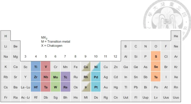
Recently, many researchers become interested in researching this TMDCs due to their properties complementary to those in graphene[8-10]. TMDCs are atomically thin semiconductors of the type MX2, where M is a transition metal of groups 4-10 (except group 8) and X is a chalcogen as shown in Fig. 1.1. One layer of M atoms is sandwiched between two layers of X atoms and each layer is usually 6~7 Å thick as shown in Fig 1.2.
TMDCs are held together by weak Van der Waals force between layers. Within each layer, the M-X bond is a covalent bond.
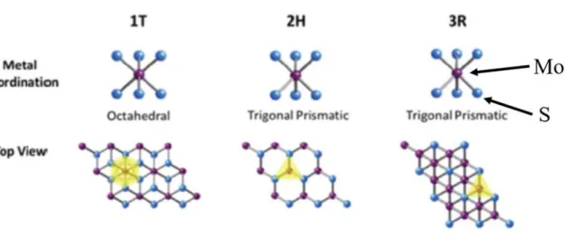
The crystal structure of single layer MoS2 is similar to that of the graphene honeycomb lattice. However, each carbon atom in graphene is replaced by Mo or a pair of S atoms for MoS2. In nature, MoS2 has three polytypes which are 2H, 3R and 1T phases[11-13]. Both 2H and 3R phases are semiconducting and have trigonal prismatic coordination[13]. However, 1T phase is metallic[14] and has octahedral coordination[13].
The 2H-MoS2, which is two layers per unit cell in the hexagonal symmetry, stacking sequence is AbA BaB (the capital represents chalcogen and the small letter represents metal in TMDCs). The 3R-MoS2, which is three layers per unit cell in the rhombohedral symmetry, stacking sequence is AbA BcB CaC. The 1T-MoS2, which is one layers per unit cell in tetragonal symmetry, stacking sequence is AbC [15] as shown in Fig. 1.3. The metal coordination and top view of this three phases are shown in Fig. 1.4.
Nature Nature chemistry vol 5 April 2013
Fig. 1.1 The transition metals and the three chalcogen elements are shown in the periodic table
Nature Nanotechnology, 2011, 6, 147-150
Fig. 1.2 Three dimensional representation of the structure of MoS2
Nature Nanotechnology, 2012, 7, 699-712
Fig. 1.3 Three polytypes of MoS2: 2H (two layers per unit cell), 3R (three layers per unit cell) and 1T (one layer per unit cell).
Chem Commun., 2017, 53, 3054-3057
Fig. 1.4 The metal coordination and top view of 1T, 2H, and 3R phase.
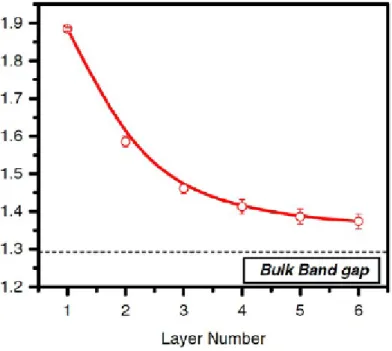
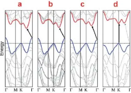
The band structures of MoS2 with different thickness, calculated by density functional theory (DFT), are shown in Fig. 1.5[16]. The lowest energy transitions are labeled by the solid arrows. For bulk MoS2 crystal, the valence band maximum is located at the Γ-point, while the conduction band minimum is located almost halfway along the Γ-K range. Therefore, bulk MoS2 is an indirect bandgap material and its bandgap is 1.29eV. When the layer number decreases, the conduction minimum moves upward and the valence band maximum (Γ-point) moves downward. However, the direct transition at K-point barely changes when the layer number decreases. Finally, MoS2 becomes a direct bandgap (~1.9eV)[2, 17, 18] material when it is a single layer. This phenomena could be explained as follows[16]: The conduction band states at the K-point are mainly composed of strongly localized d orbitals at Mo atom sites. Mo atoms are located in the middle of the S-Mo-S sandwich structure, so the interlayer coupling is weak. In contrast, states near the Γ-point and the point of indirect bandgap mainly originate from a linear combination of d orbitals at Mo atoms and antibonding pz orbitals at S atoms. Strong interlayer coupling results in the energy dependence on layer thickness. Similar changes in the electronic band structure as a function of sample thickness have been predicted for other semiconducting 2D materials[19, 20]. The MoS2 band gap energy versus layer number is
summarized in Fig 1.6[2].
Nano letter, 2010, 10, 1271‐1275
Fig. 1.5 Calculated band structures of (a) bulk (b) quadrilayer (c) bilayer, and (d) monolayer MoS2.
Phys. Rev. Letter. 2010, 105, 136805.
Fig. 1.6 Band gap energy of MoS2 as function of layer number for N= 1~6.
Because MoS2 is a semiconductor with band gap from 1.29eV to 1.9eV, it could complement graphene which is gapless in pristine condition in many electronic and photonic applications, especially for transistors[21, 22]. Furthermore, MoS2 is very sensitive to environment due to its high surface-to-volume ratio[23]. Therefore, MoS2 can easily absorb molecules on the surface. According to the charge transfer theory, charged molecules absorbed on MoS2 affect the conduction properties of the MoS2 film changing its electric characteristics[24]. MoS2 can be applied to fabricate gas sensor such as NH3, NO, biosensors for proteins or pH sensor by using these electric characteristics[25-28].
Other applications such as memory devices[29-31] and photodetectors[32] have also been reported. Some group also have made p-n diode and solar cells by using WSe2/MoS2
heterostructures[33-35]. Many applications using MoS2 have been reported widely.
1.2 Advantages of MoS
2FETs
Moore’s Law had predict the development trend of semiconductor devices and the transistor keeps scaling in the past fifty years[36]. However, it will face a serious challenge in the next few generations of transistors. With the transistor size keeps scaling down, it will encounter several bottleneck such as large leakage current, short channel effect and so on[37]. The scaling theory has predicted that a field effect transistor with a thinner dielectric and a thinner gate-controlled region will ease the short channel effect down to very short gate length[38]. This can also be understood by the concept of characteristic length[39] as shown below.
The short channel planar transistor is shown in Fig 1.7 (a) and its potential ( )x and potential energy U x( ) distribution are demonstrated in Fig 1.7 (b) and (c)
respectively. The characteristic length is defined in Eq. (1.1) and the lowest potential along the channel is shown in Eq. (1.2).
s s ox ox
t t
(1.1)
/ 2
min 2 s de Leff
(1.2)
Where is the characteristic length,
s:the permittivity of semiconductor,
ox:the permittivity of gate oxide, ts:thickness of semiconductor channel, tox:thickness ofgate oxide,
min:the lowest potential along the channel,
s:the potential in the source,
d:the potential in the drain, Leff :the effective channel length.It is obvious that having a large ratio between Leff and λ results in a smaller
min, which allows a better control of the gate when the channel scales down. Therefore, it can immune to short channel effect. While the channel length Leff scales down, a large ratio between Leff and λ requires a small λ, which means smaller channel dielectric constant, thinner dielectric and thinner channel thickness are required according to the Eq. (1.1).In order to reduce short channel effect, the channel thickness of 3D materials (such as silicon) should become thinner. However, compared with 2D materials, the roughness at the 3D materials surface will degrade mobility seriously when it becomes thinner. Even worse, the channels showing a serious thickness fluctuations lead to unacceptably large threshold-voltage variations. These problems occur even at channel thicknesses many times greater than the thickness of 2D materials. On the other hand, monolayer MoS2 not only owns ultrathin channel thickness but also has low dielectric constant compared with silicon (Si=11.9𝜀 and MoS2=3.3𝜀 ). Besides, because of no out-of-plane broken bonds
in 2D materials, there are no interface traps in the semiconductor channel and make it have a clean semiconductor-metal interface. Therefore, MoS2 has the possibility to replace silicon and result in a better FETs.
With its ultra-thin and sizable bandgap, MoS2 has been widely studied by scientists around the word. It has been reported that 15 nm gate length MoS2 transistors have on/off ratio up to 10 ~10 , subthreshold swing (SS) of 60 mV per decade, and drain induced barrier lowering (DIBL) of 10 mV/V[40]. Many device simulations have also shown that MoS2 has advantages over the scaling issue because of its immunity to short channel effect[40-42].
Fig. 1.7 (a) A simple planar structure of FET. (b)The potential ( )x distribution from the source to drain. (c) The potential energy distribution U x( ) for electrons
from the source to drain.
1.3 Motivation
As mentioned above, MoS2 material has the potential to replace the silicon. Recently, many researchers use SiO2 as a bottom gate or high k material (such as Al2O3 and HfO2) as a top gate to fabricate MoS2 transistors[43-46]. However, the field effect mobility of MoS2 transistors are around 10-65 cm2V-1s-1 which is lower than the mobility of silicon (1400 cm2V-1s-1 for electron and 450 cm2V-1s-1 for hole respectively). Furthermore, the hysteresis of MoS2 transistor is another important issue[47]. This is not desirable for logic switching applications because hysteresis increases the on/off switching voltage, thereby increasing the power consumption of the circuit[48]. In previous reports, it reports that the single or multi layers MoS2 transistor has large hysteresis when using SiO2 as an oxide layer[49-51]. Another important issue concerning the MoS2 transistor is its stability. Some reports show that the performance of MoS2 transistors would degrade after exposing to air for a long time[3].
It has been shown that the field effect mobility and hysteresis of MoS2 transistors were strongly affected by interfacial charged impurities, surface roughness on Si/SiO2
substrates and so on[3, 52]. In order to solve these problems, we will use hexagonal boron nitride (h-BN) substrate. It is a better choice which can be used to eliminate problematic
relatively free of dangling bonds, charge traps and is naturally flat[53, 54]. In addition, Single or multi layers MoS2 can easily absorb the molecules such as H2O and O2 in the atmosphere because of its high surface-to-volume ratio[55]. Therefore, we will use h-BN as a passivation layer to let MoS2 transistor have better stability and reliability.
MoS2 also has another problem in CMOS compatible issue because of its naturally n-type characteristic. Recently, possible methods to modify MoS2 has been reported[56- 59]. The major method that most scientists do is to immerse MoS2 in a fluid which can be served as a donor or acceptor[60-63]. In order to change MoS2 film to p-type, some researchers use plasma which has Fluorine or Oxygen as a p-type doping for MoS2[64- 66]. Therefore, some reports have shown that it can fabricate MoS2 rectify diode by using plasma-assisted doping as a p-region[67, 68]. However, the ideality factor of MoS2 rectify diode is 2.21[67]. In order to have better ideality factor (in the interval between 1 and 2), black phosphorus(BP) which is p-type 2D material will be used to combine with MoS2 to fabricate MoS2-BP heterostructure n-p junction.
In this thesis, the introduction of MoS2 and its development is presented in Chapter 1. The fabrication method of MoS2/h-BN heterostructure and measurement systems are introduced in Chapter 2. The exfoliation method of MoS2 and the material analysis of MoS2 before and after plasma treatment to dope the material to either p or n-type are
presented in Chapter 3. Chapter 4 presents the back-gate MoS2 TFTs with SiO2 and h-BN substrate, first. Then, we will use h-BN as a passivation layer. The air stability, hysteresis and electrical properties will also be discussed here. We will also present the characteristics of BP-MoS2 heterostructure in this chapter. Finally, the conclusions are
given in Chapter 5.
Chpater 2 Experiments
In this chapter, the fabrication system of the heterostructure devices will be first introduced. Then the measurement techniques for material analysis and annealing techniques will be presented.
2.1 Heterostructure Fabrication System
Heterosutructure fabrication system, which consists of three axis micrometer stage (Fig. 2.1) and optical microscopy, is shown in Fig. 2.2. By using this micromanipulator, the MoS2 or h-BN can be transfer to the desired position of our substrate.
After the setup of our system, we exfoliate the MoS2 flakes on the PDMS stamp (Fig.
2.3). Second, the target sample is fixed on the stage (Fig. 2.2) by using double side tape and find the position that we want to fabricate heterostructure (Fig. 2.4). Third, the PDMS stamp is inspected under the optical microscope to select the flake that we want to use (Fig. 2.5). As the PDMS is transparent, we can see the target sample through it and thus it is possible to align the desired flake on the target sample where we want to transfer the flake with sub-micrometer resolution. Finally, as the desired position is reached, we can lower the glass slide with micromanipulator and let the PDMS stamp be adhered to the target sample to fabricate heterostructue, as shown in Fig. 2.6.
Fig. 2.1 Three axis micrometer stage.
Fig. 2.2 Heterosutructure fabrication system.
Fig. 2.3 PDMS Stamp.
Fig. 2.4 h-BN flake on SiO2/Si substrate under optical microscope.
Fig. 2.5 MoS2 flake on PDMS under optical microscope.
Fig. 2.6 Heterostructure of MoS2 and hBN
2.2 Reactive Ion Etching System
Reactive ion etching (RIE) is an etching technology. There are two major etching technologies, dry etching and wet etching. RIE is one kind of dry etching, using chemically reactive plasma to remove materials on the wafers. In this study, we use RIE to generate plasma to itch the MoS2 film and put dopants on the MoS2 surface.
The operation method of RIE is illustrated in Fig. 2.7. Plasma is generated by applying a RF (13.56MHz) to the wafer platter. The strong electric field ionized the gas molecules to create a plasma. The electrons are accelerated up and down, directly attacking the wafer in the chamber.
Fig. 2.7 Diagram of RIE setup
2.3 Measurement Techniques
2.3.1 Atomic Force Microscopy (AFM)
Atomic force microscopy (AFM) is a very high-resolution type of scanning probe microscopy, with demonstrated resolution on the order of fractions of a nanometer, more than 1000 times better than the optical diffraction limit.
In this experiment, AFM is used to check the thickness of MoS2 and h-BN nanosheets by standard tapping mode, which relies on the decreasing of the oscillation amplitude when the tip comes close to the surface.
2.3.2 Raman Spectroscopy
Raman spectroscopy is a spectroscopic technique used to observe the lattice vibrational mode (phonon) of the MoS2 film. The laser light interacts with molecular
vibrations, phonons or other excitations, resulting in the energy of the laser photons being shifted up or down. Therefore, the shift in energy gives information about the vibrational modes in the system.
Raman spectroscopy occurs as a result of the atomic vibration causing a "change in polarizability" of the molecule. In contrast, Infrared spectroscopy occurs as a result of a vibration causing a change in the "permanent dipole moment". They always yield similar, but complementary information.
In this experiment, 532nm laser is used in Raman measurement. It gives the thickness information of MoS2 thanks to interlayer interactions in different thickness.
2.3.3 Photoluminescence (PL)
Photoluminescence describes the phenomenon of light emission from any form of matter after the absorption of photons. It is one of many forms of luminescence and is initiated by photoexcitation. The excitation typically undergoes various relaxation processes and then photons are re-radiated.
In this experiment, the evolution of the electronic structures of MoS2 nanosheets with various thicknesses can be reflected in their PL spectra.
2.3.4 Photoemission Spectroscopy (PES)
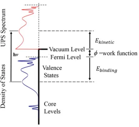
Photoemission spectroscopy (PES), also known as photoelectron spectroscopy, refers to energy measurement of electrons emitted from solids, gases or liquids by the photoelectric effect. By using different incident light, photoemission spectroscopy has two major techniques which is Ultraviolet Photoemission Spectroscopy (UPS) and X-ray Photoelectron Spectroscopy (XPS). The basic theory of photoemission presented in Fig. 2.8.
Fig. 2.8 Diagram of how photoelectron is generated.
2.3.4.1 Ultraviolet Photoemission Spectroscopy (UPS)
Ultra-violate photoemission spectroscopy (UPS) is to use ultraviolet photons to emit photoelectrons to determine the molecular orbital energies in the valence band region.
Through analysis of photoelectron kinetic energy, we can calculate the binding energy of
the specific molecular orbital energy. Besides, we can calculate the work function by using the below equation. The band diagram of an unknown material, the density of valence states and UPS spectrum are shown in Fig. 2.9.
( )
binding photon kinetic
E E E
Where Ebinding is the binding energy of the electron from the Fermi-level, Ephoton, which is hν as shown in Fig. 2.9, is the energy of the UV, Ekinetic is the kinetic energy of the electron and is the work function of the material.
In this experiment, the Fermi level and work function differences before and after plasma treatment is presented.
Fig. 2.9 The band diagram of an unknown material.
2.3.4.2 X-ray Photoelectron Spectroscopy (XPS)
X-ray Photoelectron Spectroscopy (XPS) is a quantitative spectroscopic technique that measures the elemental composition, empirical formula, chemical state and electronic state of the elements that exist in a material. XPS spectra are obtained by irradiating a material with a beam of X-rays while simultaneously measuring the kinetic energy and number of electrons that escape from the top 1 to 10 nm of the material being analyzed.
In this experiment, XPS is used to understand the element composition and atomic ratio of MoS2 bulk material.
2.3.5 Current-Voltage Characteristics
The current-voltage (I-V) characteristics of the MoS2 thin film transistor were measured by Agilent B1500A Semiconductor Device Parameter Analyzer. The field effect mobility (μEF) of the TFT can be obtained by the transconductance (gm) with a given VD. The equation of field effect mobility is shown below.
m EF
i D
g C W V
L
where W(L) is the channel width (length), Ci is the oxide capacitance per unit area. VT
can also be determined using linear extrapolation of the ID -VG plot.
2.4 Rapid Thermal Annealing (RTA)
Rapid thermal anneal (RTA) is a subset of Rapid Thermal Processing (RTP). It is a process used in semiconductor device fabrication which consist of heating single semiconductor wafers in order to improve their electrical properties.
In this Experiment, MoS2 thin film transistors were annealed by MILA 3000 Rapid Thermal Annealing Vacuum Furnace in N2 environment at 200oc for 5 minutes.
Chpater 3 Material Analysis
In this chapter, the scotch tape method to exfoliate the MoS2 film will be introduced.
Next, the material analysis for the exfoliated and bulk MoS2 will be investigated in details.
3.1 Substrate Preparation
The exfoliated MoS2 was prepared from the bulk by using Nitto tape and transferring the flakes onto a highly doped p-type silicon substrate covered by 300 nm thermally oxidized SiO2 layer. Before the transfer procedure, the silicon wafer was pre-cleaned by sonication in acetone, methanol, isopropyl alcohol and DI water each for 10 minutes.
Then, the wafers were blown dry by nitrogen gas. This process removed any residue and contaminants on the wafer. Late et al.[69] found that when the film is inspected under the optical microscope, the level of contrast depends on the thickness of the oxide layer, as shown in Fig. 3.1 (a) and (b). As the thickness of MoS2 increases, the color changes from purple to green to gold as a result of optical interference effects with the oxide layer. Just in analogy with graphene, the color contrast between MoS2 nanosheet and the underlying SiO2 is due to the interference of different wavelengths through the thin film and SiO2, as shown in Fig. 3.1 (c).
Fig. 3.1(a) Thickness dependence of color and (b) contrast in optical microscope.
(c) Optical reflection and transmission for MoS2 nanosheet with thickness d1 and refractive index n1 exfoliated on a SiO2 layer with thickness d2 and refractive index n2 grown on a heavily doped Si substrate. Nanosheets on SiO2 are visible due to interference between reflected light rays A, B and C.
(a) (b)
(c)
Advanced Functional Materials 2012, 22 (9), 1894-1905.
3.2 Preparation of Exfoliated MoS
2First, small piece of bulk MoS2 was torn off using Nitto scotch tape. Then, the Nitto tape was folded for several times in order to make the MoS2 flakes become thinner. Next, the MoS2 flakes were pasted onto SiO2/Si substrate by Nitto scotch tape. Thin flakes were attached onto substrate with scotch tape residue. The scotch tape residue was removed by acetone alcohol immersion for 1 hours. Finally, the substrate was checked carefully under an optical microscope to find out the MoS2 nanosheet with proper thickness.
3.3 Characterization of MoS
2Film Thickness
For mechanically exfoliated MoS2, it is important to locate the position of the MoS2
film first. Next, AFM can be used to accurately determine both the vertical and lateral dimensions of nanosheets. However, AFM imaging is so time consuming and of relatively slow throughput, which is unsuitable for large area inspection.
As mentioned in Sec. 3.1, optical imaging offers a simple, rapid and non-destructive characterization of large-area samples. For convenience, the optical microscopy was first used for large-scale inspection so as to select an optimal nanosheet with an appropriate thickness. After choosing the nanosheet, AFM is then used to quantitatively measure its thickness.
3.3.1 Optical Microscopy
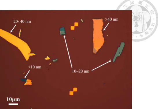
Optical contrast can be used to differentiate MoS2 nanosheets with different thickness on SiO2/Si substrates. The level of contrast depends on the thickness of the oxide layer and the optimal oxide thickness for identifying MoS2 thickness is about 300nm. Table 3.1 and Fig. 3.2 depict how the color of MoS2 nanosheets changes with its thickness on 300nm SiO2/Si substrates. The color of few layer MoS2 flakes are blue under the optical microscopy. As the thickness increases, the color changes from green to orange as a result of optical interference effects with the oxide layer.
Once a flake of interest has been located using optical microscopy, the exact thickness can be confirmed by AFM.
Table 3.1 Thickness dependence of color for MoS2 film on 300nm SiO2/Si substrate under optical microscopy.
MoS2 thickness Color
<10nm blue
10~20 nm Green
20~40 nm Yellow
>40 nm Orange
Fig. 3.2 Exfoliated MoS2 on 300nm SiO2/Si substrate under optical microscopy
3.3.2 Atomic Force Microscopy(AFM)
In this section, the color of MoS2 nanosheets changes with its thickness on 300nm SiO2/Si substrates are confirmed by AFM. Fig. 3.3 (a) displays two regions, (i) and (ii), in region (i), although the MoS2 flake has different color, we just measure its thickness in blue region. In region (ii), it has three color which are green, yellow and orange. The thickness of blue MoS2 film is 6nm as shown in Fig. 3.3 (b). The thickness of green, yellow and orange MoS2 films are 15, 23, 60nm as shown in Fig. 3.3 (c), (d), and (e), respectively. From Fig. 3.3, it verifies that the thickness correspondence table in Table 3.1 is correct. And we can use the OM image to find the proper thickness of MoS2 film that we want to use quickly.
Fig. 3.3(a) OM image of exfoliated MoS2. AFM line profile for (b) blue (c) green (d) yellow (e) orange color of MoS2 film.
3.4 Optical and Vibrational Properties of MoS
2After the thickness of MoS2 flake was measured by AFM, they were also analyzed by Raman and Photoluminescence (PL) in order to understand their optical and
vibrational properties
3.4.1 Raman Spectroscopy
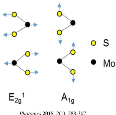
Raman spectroscopy is another useful technique to quantitatively determine the layer thickness of MoS2. The main Raman peaks correspond to the in-plane E12g and the out- of-plane A1g mode are shown in Fig. 3.4. The E12g is an in-plane mode resulting from the opposite vibration of two S atoms with respect to the Mo atom between them, while the A1g mode is attributed to the out-of-plane vibration of only S atoms in opposite directions[60]. The system used in our experiment utilizes a 532nm laser. Importantly, it is necessary to use a low laser power to prevent sample decomposition. The power used here is 50mW.
The Raman spectra of E12g and A1g mode shift as the thickness of MoS2 film changes, as shown in Fig. 3.5. For bulk MoS2, the A1g mode locates at about 407.7 cm–1 and E12g
mode is near 382.3 cm–1. The peak separation A1g - E12g = 25.4 cm–1. When the MoS2
layer thickness decreases, the A1g mode red shifts whereas the E12g mode blue shifts. The
peak separation becomes smaller. For monolayer MoS2, the A1g mode locates at about 404 cm–1 and E12g mode is near 385.3 cm–1. The peak separation is 18.7 cm–1. For 2-layer MoS2, the A1g mode locates at about 405.1 cm–1 and E12g mode is 383.1 cm–1. The peak separation is 21.7 cm–1. For 3-layer MoS2, the A1g mode locates at about 407.3 cm–1 and E12g mode is 383.5 cm–1. The peak separation is 23.8 cm–1. For 4-layer MoS2, the A1g
mode locates at about 407.5 cm–1 and E12g mode is 382.9 cm–1. The peak separation is 24.6 cm–1. Therefore, we can use Raman spectroscopy to identify MoS2 film from monolayer to 4-layer.
Photonics 2015, 2(1), 288-307
Fig. 3.4 Schematic illustration of in-plane phonon modes E12g and the out-of-plane phonon mode A1g for MoS2.
Fig. 3.5 Thickness dependent Raman spectra for MoS2.
3.4.2 Photoluminescence(PL)
Bulk MoS2 is a semiconductor with an indirect bandgap of about 1.3 eV and single layer MoS2 has a direct bandgap of ~1.8 eV[2, 17, 18]. According to density functional theory (DFT), the band structures of MoS with different thickness is shown in Fig.
3.6[16]. For bulk MoS , the direct transition occurs at K-point which has a high energy.
Therefore, bulk MoS is an indirect bandgap material. However, as the MoS layer thickness decreases, the transition between conduction band minimum and valence band
Finally, MoS becomes a direct bandgap material when it is single layer. Therefore, single layer MoS2 has a ~1.8 eV direct bandgap. With the MoS thickness increases, the bandgap of MoS2 becomes smaller and changes from direct bandgap to indirect bandgap.
Nano letter, 2010, 10, 1271-1275
Fig. 3.6 Calculated band structures of (a) bulk (b) quadrilayer (c) bilayer, and (d) monolayer MoS2.
The PL system used in our experiment utilizes a 532nm laser with a power of 5mW, measured at 300K. The bulk MoS2 showed negligible PL compare to monolayer MoS2
PL as shown in Fig. 3.7. Thinner MoS2 exhibited pronounced emissions at about 670 and 625 nm. These two peaks arise from the direct excitonic transitions at the K-point as shown in the arrow A and B in Fig. 3.8. The energy difference between these two peaks
originates from the spin-orbit splitting of the valence band energy[16]. In Fig. 3.7, the black and red line represents photoluminescence spectra for 1 and 4 layer MoS2 film, respectively. The difference of major peak position is barely changes because of the unchanged direct transition at K-point as discussed above. Furthermore, it was also shown that the PL intensity was decreased as the layer number of MoS2 nanosheets increases. In bulk MoS2, no photoluminescence is observable because of the local field effect, that is, the local electric field at a high refractive index material like MoS2 is much weaker than the incident electrical field[16].
Fig. 3.7 Photoluminescence spectra for monolayer, 4-layer and bulk MoS2.
Nature Comm., 2014, 5, 4543
Fig. 3.8 The band structure of monolayer MoS2 with the label of C calculated by the DFT. The arrows indicate the transition in A, B and the band nesting.
3.5 X-ray Photoelectron Spectroscopy(XPS)
X-ray photoelectron spectroscopy is a useful technique to determine the composition of an unknown materials. XPS is based on the photoelectric effect. Each atom has core electron with the characteristic binding energy. When the X-ray beam hits on the surface of sample, the core electron will absorb the energy of X-ray photon. If the photon energy (Ephoton) is large enough, the core electron will escape from the atom and emit out of the surface. The emitted electron with the kinetic energy Ek will be detect by energy analyzer.
Then we can use the below equation to calculate the core electron binding energy.
) (
Ebinding Ephoton Ek sp (3.1)
Where Ebinding is the binding energy of the core electron, Ephoton is the X-ray photon energy, Ek is the kinetic energy of photoelectron which can be measured by the energy analyzer and is the work function of the analyzer. Because the Fermi level of the sample and sp spectrometer are aligned, the spectrometer work function ( ) is already known. sp
Therefore, we can use above equation to get the binding energy. The band diagram of XPS is shown in Fig. 3.9.
In the section, we use XPS to analyze stability of MoS2 in air and Fermi level shift before and after plasma treatment.
Fig. 3.9 The band diagram of X-ray photoelectron spectroscopy.
3.5.1 XPS spectrum of MoS
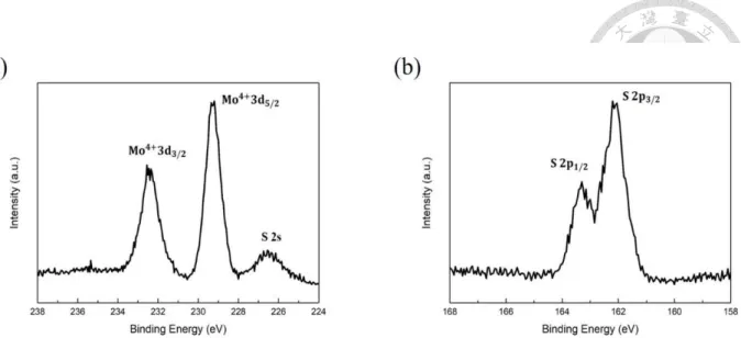
2X-ray photoelectron spectroscopy is measured in high vacuum (~108 torr) to reduce environmental interference. Fig. 3.10 (a) shows 3 peaks of Mo and S signal, one is Mo4+
3d5/2 which is at 229.3 eV, another is Mo4+ 3d3/2 which is at 232.5 eV, the other is S 2s which is at 226.6 eV. Fig. 3.10 (b) shows 2 peaks of S signal, one is S 2P3/2 which is at 162.1 eV and the other is S 2p1/2 which is at 163.3 eV.
Fig. 3.10 X-ray photoelectron spectroscopy for (a) Mo (b) S
3.5.2 Stability of MoS
2in Air
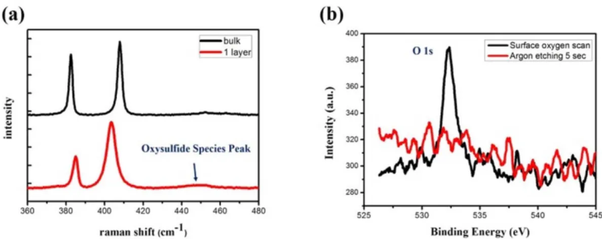
For electronic application, the stability of a material has a great impact on its reliability. Especially for 2D materials, a large surface area to volume ratio makes this issue more crucial in ambient environment. For further investigation of this phenomenon, we use Raman and XPS analysis to study this problem. Fig. 3.11 (a) shows the Raman spectra of the monolayer and bulk MoS2, it was found that a small peak appears around 450 cm-1 on monolayer MoS2, providing a supportive evidence for oxygen contaminated surface. The Raman peak at 440 cm − 1 can be ascribed to Mo-S vibrations for oxysulfide species[70]. Oxygen may attack S–Mo–S bonds. However, It shows little peak in bulk MoS2. It indicates that oxygen is only able to attack only surface layers rather than inner layer.
In order to confirm the oxygen adsorption on the MoS2 surface in air, the surface analysis of the exfoliated MoS2 by XPS was also utilized. An argon ion etching is used to etch the MoS2 surface to investigate the inner part of MoS2. Fig 3.11 (b) shows the surface oxygen scan before and after argon ion etching for 5 sec. A broad peak near 532 eV was detected before ion etching, which could be partially assigned to absorbed oxygen or water molecules. The oxygen signal was almost eliminated after argon ion etching.
Therefore, it should be noted that the oxygen layer was only in the surface rather than in the inner layer. This p type doping was reported in many research due to heavily physical adsorption oxygen[71, 72].
Fig. 3.11 (a) Raman Spectra for monolayer and bulk MoS2,respectively. (b) XPS profile of the oxygen intensity at surface and inner MoS2.
3.5.3 Material Analysis of RIE doped MoS
2In this section, we will use Reactive ion etching(RIE) as a plasma source to dope the bulk MoS2 material. Here, we will choose CHF3 gas for p-type plasma doping and the RF power is 100W, the camber pressure is 1.3pa and the gas flow rate is 10sccm during the plasma doping process.
Fig. 3.12 (a), (b), (c) display the XPS spectra of Mo 3d, F 1s and O 1s peaks before and after plasma treatment (doping time is 30s and 60s, respectively). After the plasma treatment, Mo 3d peaks shift to lower binding energy. This downshift of the peaks can be attributed to the p-doping effect because it caused the Fermi level shift toward the valence band edge and it shift about 0.4eV after plasma treatment. However, the Fermi level shift would not depend on the doping time. It shifts 0.4eV for both doping 30s and 60s.
To further identify the plasma treatment method, Fig. 3.12 (b) showed the F 1s peak before and after plasma treatment. F-related peak appeared for both 30s and 60s plasma treatment while it had no peaks on the untreated bulk MoS2. It indicated that F-contained particles are absorbed onto the MoS2 surface. In Fig. 3.12 (a), there is a new peak which is around 235eV and it corresponded to the Mo6+ signal as shown in Fig. 3.12 (d)[73]. At the same time, there is also a new O-related peak shown in Fig. 3.12 (c) after 30s and 60s
plasma attack give rise to the damage and defect on the MoS2 surface which could accelerate the oxidation process. XPS can also know the percentage of each atom. For 30s plasma treatment, the percentage of F and O atoms are 19.9% and 21.0% respectively.
For 60s, the percentage of F and O atoms are 23.5% and 20.4% respectively. Because the percentage of F and O atoms, which would induce the positive charge in the lower layer of MoS2 film and cause p-type doping, are almost the same for both doping 30s and 60s, the Fermi level shift is the same for both doping 30s and 60s as mentioned in the previous paragraph.
Fig. 3.12 The XPS spectra for (a) Mo 3d (b) F 1s (c) O 1s binding energy before and after plasma treatment. (d) The reported[73] XPS for Mo binding energy in the
MoS2 and MoO3.
3.6 Ultraviolet photoelectron spectroscopy(UPS)
Ultraviolet photoelectron spectroscopy is an useful technique to determine the electronic state of the surface region of semiconductor a sample. Comparing to XPS, it is also measured in high vacuum (~1 10 torr) to reduce environmental contamination.
In order to explain how UPS works, the band diagram of a unknown material, the density of valence states and UPS spectrum is shown in Fig. 3.13. When ultraviolet radiation with a photon energy of 10~45 eV is used, the electrons at valence levels emit. The electrons are called secondary electrons (SE). With its <50 eV photon energy, it can only excite electrons at valence states while the XPS with its 200~2000 eV photon energy can excite the electrons in the core levels. In UPS, electrons emit from valence states to vacuum level follows the equations bellow.
) (
Ebinding Ephoton Ekinctic (3.2)
Where Ebinding is the binding energy of the electron from Fermi-level, Ephoton is the energy of the UV, Ekinetic is the kinetic energy of the electron and is the work function of the
material. The kinetic energy of electrons which emit from valence states can be detected by UPS detector. When electrons come from deeper valence states, the kinetic energy becomes smaller. Therefore, the kinetic energy of electrons of the deepest valence states
equation, the work function can be extracted from SEE.
binding photon
E E
where Ekinctic0 (3.3)
On the other hand, electrons emit from valence band maximum have the largest kinetic energy. Through UPS analysis, the binding energy between valence band maximum and Fermi-level can be extracted.
Fig. 3.13 Band diagram of an unknown material.
3.6.1 Work Function of MoS
2The UPS spectrum of MoS2 is shown in Fig. 3.14 (a). To further investigate the spectrum, we fit the lines to extract binding energy for the zero and maximum kinetic energy of emitted electrons which are shown in Fig. 3.14 (b) and Fig. 3.14(c). In Fig 3.14 (b), the binding energy which corresponds to the secondary electron edge (SEE) is 16.7 eV. From the SEE at which the kinetic energy of emitted electron is zero, the work function of bulk MoS2 can be calculated to be 4.45eV. In Fig. 3.14 (c), we can extract the smallest binding energy which means these electrons are emitted from the valence band maximum. Therefore, the energy between valence band maximum and Fermi-level is 1.2 eV. Because bulk MoS2 has an indirect bandgap about 1.3 eV[16], the Fermi-level is close to the conduction band with about 0.1 eV energy difference that indicates the n-type characteristic of MoS2 layer. And the band diagram of bulk MoS2 is shown in Fig. 3.15.
Work function = (photon energy of He‐I lamp radiation) – (binding energy of SEE)
=21.2eV – 16.75 eV = 4.45 eV
Fig. 3.14 (a), (b) and (c) UPS spectra of pristine MoS2
Fig. 3.15 Band diagram of bulk MoS2
3.6.2 Material Analysis of RIE doped MoS
2In this section, we will use the same sample as mentioned in Sec. 3.5.3 but using UPS to analyze the work function difference before and after RIE doping.
In Fig. 3.16 (a) and (b), the binding energy which corresponds to the secondary electron edge (SEE) of plasma treatment MoS2 for 30s and 60s are 16.6 eV and 16.48 eV respectively. Therefore, we can calculate the work function is 4.6 eV and 4.72 eV respectively. In Sec. 3.5.3, we know that the Fermi level shift either for 30s or 60s plasma treatment MoS2 are 0.4 eV. However, the increased work function is 0.15 eV and 0.27 eV respectively rather than 0.4 eV. It is because that the MoS2 will easily absorb the carbon in the atmosphere after plasma treatment. The information that we can acquire from the UPS is just in the sample surface about 1-3nm. Therefore, the carbon which is absorbed on the MoS2 surface would influence the measurement of UPS and let the vacuum level shift to the conduction band as shown in Fig. 3.17.
Fig. 3.16 UPS spectra for (a) 30s (b) 60s plasma treatment
Fig. 3.17 The band diagram of (a) pristine (b) plasma treatment for 30s (c) plasma treatment for 60s MoS2.
Chpater 4 MoS 2 Thin Film Transistors
In this chapter, the fabrication processes and the electronic properties of back-gated MoS2 TFT will be first described. Then, SiO2 substrate will be replaced by h-BN substrate in order to improve the mobility and reduce the hysteresis. The same MoS2 flake with and without h-BN as a bottom gate would be fabricated to compare the properties of these two TFTs on the different substrate. Finally, the MoS2 rectify diode and MoS2-Black Phosphorus n-p heterojunction was fabricated and theirs electronic and optical properties will be measured and discussed.
4.1 MoS
2Back-gated TFTs using SiO
2Substrate
In this section, the fabrication processes and the electronic properties of MoS2 back- gated TFT using SiO2 substrate will be described.
4.1.1 Device Process Flow
Because it is very hard to locate the position of the chosen flake on the substrate during the processing steps of the devices. Therefore, a two-digit number system was used to define our pattern on the 300nm SiO2/p++ Si substrate by photolithography followed by thermal evaporation of Cr (5nm)/Au (80nm) contact metal and lift off process,