國立臺灣大學電機資訊學院資訊工程學系 碩士論文
Department of Computer Science abd Information Engineering College of Electrical Engineering and Computer Science
National Taiwan University Master Thesis
如何用頁面重寫降低快閃記憶體中錯誤更正碼的成本 How to Reduce The ECC Cost of NAND Flash Memory
With Page Rewriting
廖書賢 Shu-Hsien Liao
指導教授:郭大維博士, 張原豪博士
Advisor: Tei-Wei Kuo, Ph.D. , Yuan-Hao Chang, Ph.D.
中華民國 107 年 6 月
June 2018
中文 要
近年來,快閃記憶體的儲存密度逐漸上升。新興的高密度裝置,像 是多級單元或三級單元的可靠度比較低,所以需要較強的錯誤更正碼 以承受更多的寫入/抹除次數。然而較強的錯誤更正碼需要額外空間及 效能的管理費用,且他需要昂貴的硬體支援。若裝置可以在固定的寫 入/抹除次數中承受更多次的寫入的話,裝置的寫入/抹除次數以及錯誤 更正碼成本的需求就可以被減緩。在此篇論文中,我們提出了一個考 慮干擾的頁面重寫機制並使用他來儲存熱數據,使裝置在固定寫入/抹 除次數下可以承受更多次的寫入。我們將會藉由一系列的實驗驗證此 機制的能力。最後結果顯現出藉由我們提出的機制,我們可以讓裝置 不犧牲耐久度的情況下減少寫入/抹除次數以及錯誤更正碼的需求成 本。
關鍵字:快閃記憶體,耐久度,重寫,錯誤更正碼,系統
Abstract
The density of NAND flash device continues to increase in recent years.
Emerging high density devices like MLC or TLC has lower reliability and re- quires stronger ECC to tolerate more number of P/E cycle. However, strong ECC brings space and performance overhead, and it requires costly hardware support. If the device can tolerate more number of writes within fixed P/E cycle, the P/E cycle and ECC requirement can be relaxed. In this work, we propose a disturbance-aware page rewriting and use it to store write-hot data so that the number of write operations a device can tolerated within fixed P/E cycle can be improved. The capability of the proposed design is evaluated by a series of experiments, and the results show that with our proposed design, the P/E cycle as well as the ECC requirement can be reduced without sacri- ficing its endurance.
Keywords : NAND flash memory, Endurance, Rewriting, Error Correc- tion Code, System
Contents
會 定書 i
中文 要 ii
Abstract iii
Contents iv
List of Figures v
List of Tables vi
1 Introduction 1
2 Background And Motivation 4
3 Disturbance-Aware Page Rewriting Design 8
3.1 Design Overview . . . 8
3.2 Disturbance-Aware Page Rewriting . . . 11
3.3 Address Translation . . . 11
3.4 Disturbance Handling . . . 12
3.5 Garbage Collection . . . 16
3.6 Overhead Analysis . . . 16
4 Experiment Results 18 4.1 Experiment Setup . . . 18
4.2 Experiment Results and Discussion . . . 19
5 Conclusions 23
Bibliography 24
List of Figures
1.1 Typical system architecture of NAND flash memory . . . 2
2.1 Threshold voltage distribution and representing logic values of MLC and TLC flash . . . 6
2.2 Illustration of Rewritable Programming Design . . . 6
3.1 System architecture with the proposed page rewriting design . . . 9
3.2 An example of write-hot data mapping in rewritable blocks . . . 12
4.1 Endurance result for 3 selected traces . . . 20
4.2 Page migration due to disturb analysis for 3 selected traces . . . 21 4.3 Page migration due to disturb analysis for 3 selected traces (When TD=2) 21
List of Tables
3.1 Description of parameters used in our mechanism . . . 13
4.1 Configuration of the simulated flash-based SSD . . . 18 4.2 Parameters of simulated experiments . . . 18
Chapter 1 Introduction
NAND flash storage devices such as solid-state drive (SSD) gain more market share in recent years. As the growing need of high capacity, Multiple/Triple Level Cell (MLC/
TLC) flash memory with two or three bits per cell are becoming more popular than Single Level Cell (SLC) that stores only one bit per cell. Compared to SLC, MLC/TLC devices have the advantage of lower cost since their density is higher, but their reliability is sacri- ficed as they have higher raw bit error rate. To cope with the bit errors, a more complex Error Correction Codes (ECC) is needed for high density flash memory devices so that the device can tolerate more number of program/erase cycle (P/E cycle) before it wears out. The maximum P/E cycle modern 2x-nm MLC and TLC NAND flash can endure are merely 3k and 1k respectively [1].
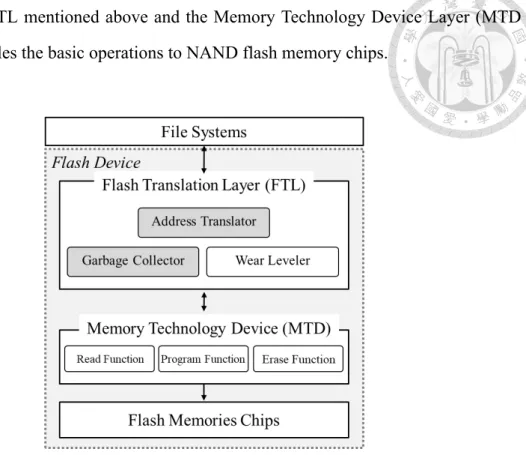
A flash storage devices usually consists of several flash memory chips. Each chip contains many flash blocks, and there are a fixed number of pages in a block. An erase operation is done in the unit of a block, while a read or a program operation is done in the unit of a page. A page usually contains a data area for storing user data and a spare area for house-keeping information such as ECC and page status. Once a flash page is pro- grammed, it cannot be programmed again until its residing block is erased, this is known as the write-once property. Thus, to update a data page, out-place update is adopted to write the new data to an empty page and invalidate the old data page. Therefore, the flash device need to manage the mapping between logical address and physical address, which is done by the flash translation layer (FTL) in the flash controller. When the flash device is running out of space, FTL performs garbage collection (GC) to reclaim invalid spaces caused by the out-place update. FTL also contains wear leveling design to evenly dis- tribute write requests to every flash blocks. Figure 1.1 shows the typical flash architecture
including the FTL mentioned above and the Memory Technology Device Layer (MTD layer) that handles the basic operations to NAND flash memory chips.
Figure 1.1: Typical system architecture of NAND flash memory
To ensure certain number of P/E cycle, the ECC requirement for high density flash de- vices like MLC or TLC is higher. However, providing a stronger ECC not only wastes a significant extra space but also hurts the I/O performance since it requires a longer decod- ing time. Besides, a complex and costly hardware is also needed to support such stronger ECC. In fact, the endurance of flash device can be rated more precisely by the total num- ber of writes the device has tolerated over its entire life instead of P/E cycles. That is, we can reduce the P/E cycle and ECC requirement without sacrificing its endurance as long as the device is able to tolerate more number of writes per P/E cycle. This motivates us to explore the possibility of increasing the number of writes a NAND flash device can tolerated by a different programming techniques.
In this work, we propose a disturbance-aware page rewriting strategy to lower the ECC cost without sacrificing the endurance of the device. The main concept is to enable each page to be programmed several times without the need of erasing its residing block. By doing so, the number of write operations the device can tolerated before it wears out can be
largely increases. The proposed page rewriting has a constraint that previous data should be invalidated before it can be re-programmed again, so it is suitable for certain type of data (i.e. write-hot data). The address translator is modified to fit the write-hot data map- ping. Since the error results from program disturbance could be worsen, a disturbance handler is also needed to lower the impact of program disturbance. Overall, the FTL and MTD layer are redesigned for the proposed disturbance-aware page rewriting.
The rest of the paper is organized as follows. Section 2 presents the research back- ground and motivation. Section 3 presents the proposed disturbance-aware page rewriting design. Section 4 evaluates the capability of the proposed design by several experiments.
And Section 5 concludes this work.
Chapter 2
Background And Motivation
As flash density increases, the reliability of NAND flash memory is getting worse. As a result, various type of error patterns [2] should be taken care of. When programming a flash page, its neighbor pages might be affected due to parasitic capacitive coupling [3].
This is known as program disturbance. The voltage distribution of cells suffering from program disturbance tend to shift right to higher voltage state. Program disturbance error occurs when the victim cells are disturbed several times and their voltage distributions shift to other state. In multi-level cell flash devices, a wordline contains more than one page, so a page may be disturbed several times, leading to more severe program distur- bance than SLC. In order to lower the impact of program disturbance, the FTL usually allocates pages in specific order [4].
As flash density increases, the flash cells become more unreliable, thus the guaranteed P/E cycle of each flash block is smaller as we discussed in Section 1. However, it is not precise enough to rate the endurance of NAND flash memory by P/E cycle. Instead, it is more accurate to evaluate the endurance by showing how many bytes can be written to the flash over its entire life. Flash endurance is commonly rated by either Drive Writes Per Day (DWPD) or Tera-bytes Written (TBW), both of them are defined by JEDEC [5].
We will use the latter one as the endurance metric in the rest of this paper.
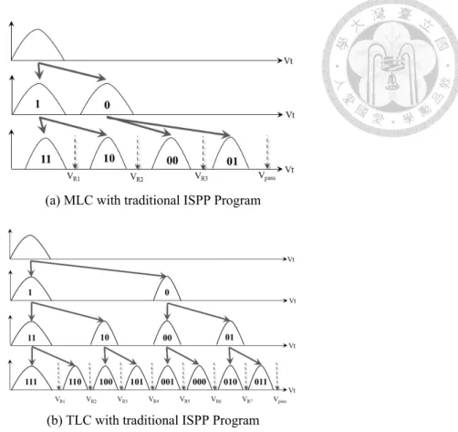
The program operation of NAND flash memory is composed of many steps. During the programming process, the threshold voltage of every cells in the programmed page are gradually increased and verified until they exceed their target voltage. This program-
and-verify process is known as incremental step pulse programming (ISPP) algorithm [6].
After the final step of ISPP, the threshold voltage is separated into 2N distributions rep- resenting N bits of logic values. Figure 2.1 shows the logic values of MLC and TLC separately. In the rest of the discussion, we will use traditional ISPP programming algo- rithm to represent the algorithm mentioned above. Except the traditional ISPP program- ming algorithm, various effective programming techniques were proposed to improve the programming efficiency or the reliability [3, 7–11]. Some proposed to enabling subpage program when storing data with smaller size so that the GC overhead can be reduced [10].
Others proposed to rewrite a block multiple times without erase for SLC NAND flash memory [7, 9] so as to increase the endurance. The concept of virtual erase and various rewritable programming designs are proposed in [7]. Figure 2.2 illustrates the rewritable programming design. Pages in a block can be rewritten again once they are all invalid pages. A block can be rewritten multiple times before the VTreaches the Vpass. The major advantage of programming by rewrite is that the number of write operations a block can tolerate before it wears out can be increased, so the overall endurance can be enhanced.
Due to its constraint, that all data pages in this block should be invalidated before it can be rewritten again, makes it difficult to manage and apply for general usages.
How to manage the write requests in NAND flash memory is one of the most critical issues in the flash design. Since a flash block has limited P/E cycle, a bad write man- agement will result in higher write amplification and the flash device will wear out even faster. To manage the write requests efficiently, we often separate data in write requests into write-cold data and write-hot data. The former one is seldom updated, while the latter one has higher update frequency. Previous work shows that write-hot data have similar characteristics in most of the applications [12]: First, a very small portion of the data are write-hot data (ie.e, less that 1%). Second, although the amount of write-hot data is rel- atively small, these write-hot data receive the vast majority of the write requests. The authors observed that for ten of the selected sixteen applications, only 1 % of the write- hot data receive nearly 100% of the write requests. Thus, how to program these write-hot
(a) MLC with traditional ISPP Program
(b) TLC with traditional ISPP Program
Figure 2.1: Threshold voltage distribution and representing logic values of MLC and TLC flash
data will have a huge impact on the endurance of NAND flash memory. Unfortunately, storing write-hot data with traditional ISPP algorithm and out-place update has negative effect on endurance. The reasons are twofold: (1) Due to out-place update constraint, whenever a write-hot data page is updated, an invalid page is formed. Due to the high up- date frequency of write-hot data, blocks storing write-hot data will be filled with invalid pages soon. (2) Since blocks become full rapidly, garbage collection will be triggered frequently in order to reclaim those invalid pages. However, execute garbage collection frequently will result in worse system performance and endurance. Therefore, some also
Figure 2.2: Illustration of Rewritable Programming Design
proposed to improve the system performance and endurance of NAND flash memory by reducing the GC overhead. [13, 14].
This work is inspired by the above observation that storing write-hot data with con- ventional ISPP algorithm and out-place update has negative effect on the endurance of flash device. Replace ISPP algorithm with rewrite seems to be a good solution since it allows a block to be programmed multiple times without erase operation. However, to fit real applications, the rewrite operation should be extend to page granularity, that is to say, each page should be rewritten separately without considering whether other pages in the same block is a valid page or not. We find that the characteristic of page rewriting makes it a good solution for storing write-hot data: (1) It has the advantage of allowing each page to endure additional number of program operations before their residing block requires an erase operation. (2) The constraint that previous data should be invalid is re- laxed since write-hot data are updated frequently and their older version data pages will be invalidated. (3) A block applying page rewriting must be an SLC block, but the draw- back of decreasing bit density is negligible since only small amount of data are write-hot data. Different from existing works that focus on how to program a page multiple times without erase operation or how to increase the number of rewrite, we are interested in exploring how to redesign the overall system so that we can apply the rewrite operation in page granularity, and then we will use the proposed page rewriting scheme to store write-hot data so that the TBW can be increased within fixed P/E cycle. To achieve this goal, the technical issues falls on how to apply page rewriting and resolve the potential program disturbance issue simultaneously. With the proposed page rewriting scheme, the issue of storing write-hot data can be solved by providing more number of writes within fixed lifespan, which means we can relax the guaranteed P/E cycle requirement as well as the ECC hardware cost without sacrificing the endurance of the flash device.
Chapter 3
Disturbance-Aware Page Rewriting De- sign
In this section,a page rewriting scheme is proposed to reduce the ECC cost by achiev- ing same number of write endured within smaller P/E cycle. The first key point of the proposed scheme is to enable rewrite operation in page granularity. Since page rewriting allows each page to be programmed multiple times, we will program write-hot data with page rewriting technique. The second key point of the proposed scheme is to alleviate the impact of deteriorated program disturbance. We have to add two features, disturbance detection and disturbance correction into the write policy managed by FTL. We first intro- duce the system architecture and the basic of page rewriting operation (Section 3-1). We then explain the FTL design for supporting page rewriting in detail (Section 3-2). Next, we discuss the overhead analysis of the proposed design (Section 3-3).
3.1 Design Overview
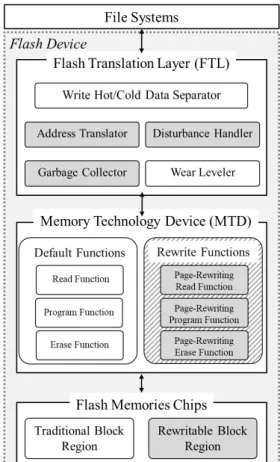
Figure 3.1 shows the system architecture of NAND flash device. To enable rewrite op- eration in page granularity, the MTD layer has to support a different set of read, program and erase functions. The rewrite operation introduced in Figure 2.2 is extended to page granularity, and the main difference is that a page, instead of a block has to be invalid so that the next rewrite operation can be performed. As you can see, there are two types of block in the flash chips. Blocks programmed by traditional ISPP programming are named traditional blocks; while blocks programmed by the proposed page rewriting are named rewritable block. When FTL receives a write request, it will identify whether the to-be-
Figure 3.1: System architecture with the proposed page rewriting design
written data is a write-hot data or a write-cold data. This identification is done by the write hot/cold data separator using existing hot/cold data separation methodologies [12]. The address translator will then map write-cold data and write-hot data to traditional blocks and rewritable blocks respectively. The reason behind this is that the characteristics of the proposed page rewriting make it suitable for storing write-hot data as we mentioned in Section 2. To manage the flash blocks, we have to decide whether the type of each flash block should be fixed or changeable. If we fix the type of every block once the device is manufactured, rewritable blocks will wear out much more faster than traditional blocks since write-hot data receive the vast majority of the write requests [12]. Obviously fixing the block type is not feasible due to wear imbalance, thus the type of each block should be changeable. To achieve this goal, all flash blocks should support both type of functions defined in MTD layer. Besides, when a block is reclaimed by garbage collector, the block can be configured to either a traditional block or a rewritable block based on the status of each region. The detail of garbage collector will be explained in Section 3.5. To simplify
the discussion, we adopt page-level mapping, dynamic wear leveling, and greedy garbage collection in our model.
For rewritable blocks, the available number of rewrite operations per page varies de- pending on many factors including the size of the maximum VTand the reliability of flash device. The reliability, however, is also related to many factors including the hardware quality and the software management design of flash device. As a result, in the rest of this paper, we will use K to denote the available number of rewrite operations per page, and every page in a same rewritable block has a same value of K. We use BKto represent a rewritable block B that every page can be rewritten K times. For simplicity, we assume every rewritable block has a same value of K in our model as well. Since there are many hardware technology of flash device and they differ in reliability, vendors should know what is the maximum value of K their product can achieve. For example, a 75nm SLC flash memory can endure up to 6-time rewrite operations [7]. High density flash devices like TLC with 3D technology []are expected to achieve a larger K since the original num- ber of threshold voltage windows is 8. To endure more program operations than a TLC (3-bit per cell) flash, the value of K should be larger than 3. We compare the ideal TBW of a TLC block and a rewritable block BKin the following equations:
TBWTLC = 3 bits× W Ls × Spage× P EC
W AF (3.1a)
TBWBK = 1 bits× W Ls × Spage× P EC × K
W AF (3.1b)
WLs is the number of word lines per block, and Spagerepresents the size of a physical page, so bits× W Ls×Spage represents the capacity. The guaranteed P/E cycle is denoted as PEC, and WAF is the write amplification factor results from flash management overhead.
Since WLs is the same for both types of block, when K is larger than 3 and there’s no significant difference in WAF, a rewritable block can achieve same TBW of a TLC block under smaller P/E cycle.
3.2 Disturbance-Aware Page Rewriting
In this section, we will introduce the proposed page rewriting in detail including how address translator (Section 3.3), disturbance handler (Section 3.4), and garbage collector (Section 3.5) are designed. To simplify the discussion later, we use R to denote the number of rewrite operation a page has endured.
3.3 Address Translation
Algorithm 1 shows the procedure of address mapping. The main concept is to map data with same logical address, different version to a same physical page address(PPA).
Since the data stored in rewritable blocks are frequently updated write-hot data, when we update a data, its older version data that stored in the rewritable block becomes useless and can be invalidated. Since the page storing that data is invalid, it can be used for next page rewriting operation. When a write request comes and it is identified as write-cold data, it will be written in the traditional region with conventional address mapping and program- ming algorithm (Line 1-2). While if it’s a write-hot data, the address translator first try to check whether an valid and old version of the requested data in the rewritable region (Line 5-6), if not, an empty rewritable page will be allocated (Line 7). Otherwise, if the data was not in rewritable region or it was in rewritable region but there’s not enough space for rewriting again, the address translator will also assign an empty rewritable page for it (Line 8-14). If there’s old version of that data and there’s still voltage space to rewrite that page, the data can be updated in-place so the address mapping remains unchanged (Line 15-16). Before the physical write operation starts, the data in the old physical page address can be invalidated (Lline 18).
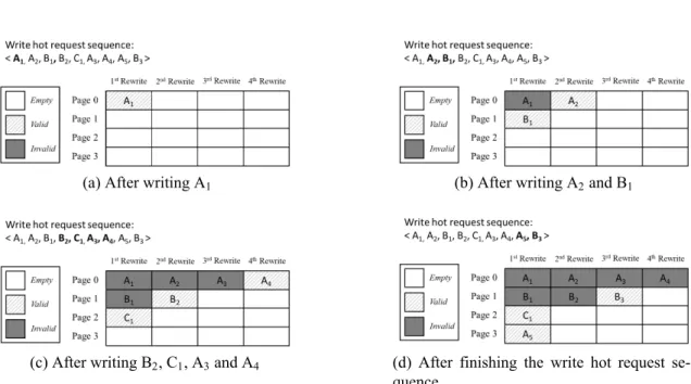
The address translation can be better explained in Figure 3.2. The nth version of data
X is denoted as Xnin our example. We consider a write-hot request sequence of <A1, A2, B1, B2, C1, A3, A4, A5, B3>. When A1 is written, since there’s no old version of A in the rewritable region, the address translator will map it to an empty page (i.e. Page 0) as shown in Figure 3.2a. When we want to update A from A1 to A2, we first find the PPA of A1 with the help of FTL, then A2 can be rewritten to the resident page of A1 and A1
will be invalidate (Figure 3.2b). When some data are updated over K times (i.e. K=4, data A in Figure 3.2c), the page storing that data is no longer rewritable before this block is erased and reclaimed. In this case, if another request of writing that data comes, the address translator will find a new empty page and program that data to a new PPA (i.e. A5 in Figure 3.2d), which is similar to the out-place update in traditional ISPP programming algorithm. Note that although a page can be rewritten for several times, the number of valid page per wordline is always 1.
(a) After writing A1 (b) After writing A2and B1
(c) After writing B2, C1, A3and A4 (d) After finishing the write hot request se- quence
Figure 3.2: An example of write-hot data mapping in rewritable blocks
3.4 Disturbance Handling
In traditional ISPP programming algorithm, pages are allocated and programmed un- der specific order so that the number of program disturbance to each word line can be
minimized [3]. However, for rewritable blocks, the program order depends on the write- hot data request sequence, thus it is unpredictable. Since the program order and cannot be restricted, some rewritable pages could suffer from more severe program disturbance. For example, in Figure 3.2c, C1in Page 3 is first written and hasn’t suffered any disturbance yet. But after writing B3and B4as shown in Figure 3.2d, C1will be disturbed for 2 times, which might lead to a high raw bit error rate that might be uncorrectable by ECC. As a result, we have to design disturbance handler to detect and correct the potential victim pages of program disturbance. Since the maximum R of every page is K, the maximum number of disturbance a page would receive from its neighbor page is 2× K for planar NAND flash device.
Parameter Description
K Available number of rewrite operations per page R Number of rewrite operations a page has endured ND Number of program disturbance a page has received TD Maximum number of program disturbance a page can
tolerate before an uncorrectable disturbance error occurs Q Rewrite quota left for a page
RE Reclaiming efficiency of a block
Table 3.1: Description of parameters used in our mechanism
Algorithm 2 shows the procedure of the proposed disturbance-aware page rewriting combining with the disturbance handler. When a page is disturbed by any of its neigh- bor pages, its threshold voltage tends to shift toward right [4]. The amount of Vth shift is proportional to the number of program disturbance the victim page received. We use NDto denote the number of program disturbance received, and NDis recorded for every rewritable page. NDof a page is reset to zero when this page is rewritten (Line 3) or when the block this page resides in is erased. As what we have mentioned in Section 3.1, the reliability varies with the devices, and so is the tolerance to program disturbance. Thus, we define a threshold value, TD, representing the maximum number of program distur- bance a page can tolerate before an uncorrectable disturbance error occurs. Whenever a
Algorithm 1: Address Translator
1 if detected as write-cold request then
2 Write in traditional region;
3 else
4 // Case : Write-hot data
5 Address translation to find the physical address of this LBA;
6 if there doesn’t exist a valid, old version of the requested data in PPAoldthen
7 Get an empty rewritable page as PPAtarget;
8 else
9 if PPAoldis at traditional region then
10 Get an empty rewritable page as PPAtarget;
11 else
12 // Case : the old version data is stored in a rewritable page
13 if R of page in PPAold>= K then
14 Get an empty rewritable page as PPAtarget;
15 else
16 PPAtarget= PPAold;
17
18 Invalid the data in PPAold;
19
20 PAGE_REWRITE(requested data, PPAtarget);
21
rewritable page is programmed, the NDof its neighbor pages should be increased (Line 8).
Note that we increase the NDof neighbor pages only when the R of that page is smaller than the R of the programmed page (Line 6), because the program disturbance is usually negli- gible when the programmed voltage is smaller than the stored threshold voltage [15, 16].
If the disturbance handler detects that the NDof a page reaches the defined threshold TD after the increase, then this page is viewed as a potential victim of uncorrected disturbance error and it should be corrected immediately (Line 9-17). The correction can be done by two approaches: (1) Rewrite this page again, (2) Invalid the original page and program this page to an empty rewritable page. Note that both approaches requires a program operation and will also disturb the neighbor pages of the target page, the only difference is the programmed address.
When disturbance correction is needed, if the target page is only programmed once, applying the first approach might be better since R of this page is only 1 and there’s still
many voltage space to rewrite. However, if data stored in the target page have much lower update frequency than its neighbor pages, it could be viewed as a potential victim for several times since it is seldom rewritten and its NDis less likely to reset. Therefore, the target page will stuck in a vicious cycle of being disturbed and corrected by first approach again and again. In this case, correct this target page by the second approach seems to be a better solution. Thus, we give each rewritable page a rewrite quota Q, where Q is set to Qmax whenever its residing block is reclaimed. A rewritable page suffering from disturbance could be corrected by the first approach for Q times (Line 9-12). If a target page requires to be corrected but it is running out of quota, the disturbance handler will correct it by the second approach (Line 13-17). Table 3.1 summarizes all the parameters used in Section 3, and Algorithm 2 .
Algorithm 2: PAGE_REWRITE Input: data, addr
Output:
1 Write data to Page in addr;
2 Increase R of Page in addr by 1;
3 Reset NDof Page in addr to 0;
4 // Disturbance Handler
5 foreach P agex ∈ Neighbor pages of Addr do
6 if R of P agex ≧ R of Page in addr or P agexis not a valid page then
7 continue;
8 Increase NDof P agexby 1;
9 if NDof P agex > TDand Q of P agex> 0 then
10 // Case : detect disturbance, correct by rewrite again
11 Decrease Q of P agexby 1;
12 PAGE_REWRITE( data in P agex, PPA of P agex);
13 else if NDof P agex> TDand Q of P agex<= 0 then
14 // Case : detect disturbance, correct by page migration
15 Get an empty rewritable page as PPAtarget;
16 PAGE_REWRITE( data in P agex, PPAtarget);
17 Invalid P agex
18 else
19 // No disturbance is detected, do nothing;
20 21 end
3.5 Garbage Collection
When the empty space of either region is beyond certain threshold, garbage collection should be triggered to select and reclaim victim blocks for that region. To select a victim block, all non-empty blocks in either region should be considered since we allow the type of every block to be changeable. Existing greedy garbage collection select a block with highest number of invalid pages so that the live page copy overhead and the write ampli- fication could be minimized. However, from Equation 3.1 we know that the capacity of a TLC block and a rewritable block is different since the bit per cell is 1 and 3 relatively. As a result, the victim block selection should consider not only the number of invalid pages but also the size of that block. We use reclaiming efficiency (RE) defined in Equation 3.2 in victim block selection. A block with highest reclaiming efficiency has largest percent- age of invalid pages and hence will be selected during garbage collection. When there is a tie, the garbage collector will select the block with smaller P/E cycle for better wear leveling.
RE = T otal size of invalid space
T otal size of the block (3.2)
3.6 Overhead Analysis
When a TLC block is configured to a rewritable one, the overall capacity of the device will be decreased since the bit per cell is decreased from 3 to 1. The capacity loss of one single block is 66%. However, this is acceptable, since we require a rewritable block only when there’s a need to store write-hot data. And as what we have mentioned in Section 2, only very small fraction of data are write-hot data. In fact, we find that configuring 10%
of the blocks or even fewer to rewritable region is sufficient enough for all applications in our experiments. That is, the maximum capacity loss of our mechanism is only 6.67%.
Figure ?? shows the relationship between capacity loss and the percentage of rewritable block among every block when the traditional blocks are 3-bit TLC.
The proposed mechanism requires additional memory to keep the FTL management information. The size of every parameters is related to the value of K. Since the threshold voltage a flash cell can store is limited within a range, the range of K will be limited as well, and we assume the maximum value of K is 15. The maximum value of R and Q should not be greater than as K, while the maximum value of ND and TD should not be greater than 2× K since a rewritable page will be disturbed by two of its neighbor pages and at most K times per neighbor page. As a result, all the parameters mentioned can be stored in a 1-Byte integer. Storing K, TD, and Qmaxrequires only O(1) memory space so they can be ignored. While R, ND, and Q are stored for every rewritable pages, so the memory overhead for storing them should be calculated, and it is related to the number of rewritable pages. For example, for a 128 G-bits flash device with roughly 5.5K blocks, where the number of pages per block is 384 [17] and the number of pages per rewritable block should be 128. If 10% of the blocks are configured to rewritable blocks, then the memory usage for storing R, ND, and Q will be 5500× 0.1×128×1×3 Bytes, which is only 0.2MB and is an acceptable additional memory usage.
Chapter 4
Experiment Results
4.1 Experiment Setup
Flash Size 128 GB
Block Size(TLC) 3 MB
Page Size(TLC) 8 KB
P/E cycle 1000
Initial % of rewritable blocks 10 %
Table 4.1: Configuration of the simulated flash-based SSD
Parameter Value
K {6,8,10}
Q {0,2}
TD {2,4}
Table 4.2: Parameters of simulated experiments
In this section, we evaluate our proposed disturbance-aware page rewriting design with a trace-driven flash simulator. Three public traces (i.e. the media server, project server, and proxy server) obtained from the Microsoft Research Cambridge [18] are used to evaluated the capability of our design. As shown in Table 4.1, a 128 GB TLC flash device is simulated as our baseline. The size of each block and page are 3MB and 8KB respectively, which is referenced from the specification of Samsung V-NAND flash [17].
The maximum guaranteed P/E cycles of each block is 1000. Furthermore, we repeat the trace until any block’s P/E cycle exceeds the P/E cycle limitation since uncorrectable error is likely to occur. As for our proposed strategy, we configure 10% of the blocks as rewritable type initially since we know that for most of the applications, the ratio of write-hot data is relatively small. As a result, there are about 39K traditional TLC blocks
and 4K rewritable blocks in total initially, where the number of pages per block is 384 and 128 respectively. Note that the ratio of rewritable blocks to all blocks will be dynamically changed during run time since the type of each block can be re-decided when reclaimed.
Besides, the block size of the rewritable block will be 13 of the traditional TLC block since the density of the rewritable block is decreased to 1 bit per cell.
Table 4.2 summarizes all configuration parameters we are going to simulate. Note that we use Q to denote the Qmaxmentioned in Section 3.4, which is the default value of the rewrite quota Q. The selection of TD is 2 and 4, representing a low reliability and a high reliability device respectively as we know that an MLC page being disturbed 4 times is likely to have disturbance error [4]. Besides, we find that when the reliability is low (TD=2), increasing the initial value of rewrite quota Q has negative effect on endurance.
Therefore, we will only compare the result of Q=0 (No rewrite quota is given) when TD is configured as 2 in the rest of the experiments.
4.2 Experiment Results and Discussion
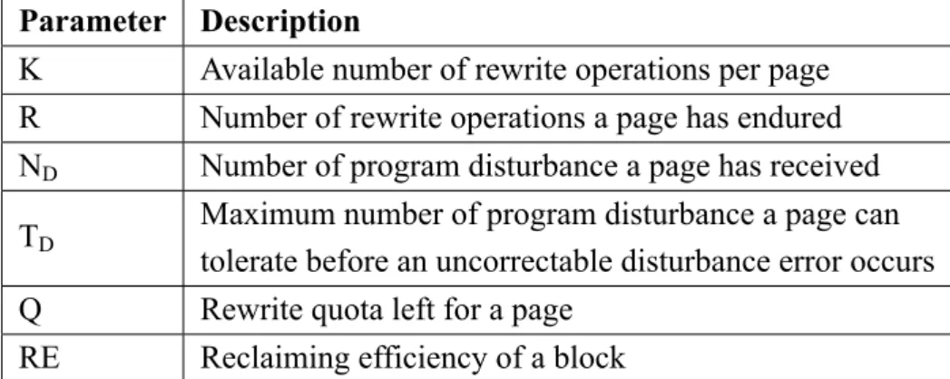
Figure 4.1 shows the accumulated TBW (normalized) of every traces with all set of configurations. Each line represents a set of configuration parameter, where the blue dot- ted line is the final TBW of baseline (TBWBase) normalized to 1. The x-axis is the maximum P/E cycle among all blocks, where the y-axis represents the accumulated TBW normal- ized to TBWBase. As you can see, three configuration parameters have similar influence on all the selected traces. First, when K becomes larger (i.e. from 6 to 8 or 10), the TBW will increase. Second, when the device is more reliable (TD from 2 to 4) and can endure more number of program disturbance from neighbor page program, the endurance result will be better as well. For device with TD=4, increasing Q from 0 to 2 results in signifi- cant improvement on the endurance. For all three traces, the configuration parameter set {K=10, Q=2, TD=4} has the best results, their TBW gain are 1.27, 1.31 and 2.21 times better than the baseline respectively. On the other hand, with our proposed design, the
(a) Media Server
(b) Project
(c) Proxy
Figure 4.1: Endurance result for 3 selected traces
ECC requirement can be reduced without sacrificing the endurance (TBW). When the best configuration parameter set is used, in order to reach the same endurance of the baseline, the P/E cycle requirement for meeting the TBWBaseare roughly 870, 780, and 470 respec- tively. Since the P/E cycle requirement can be relaxed, the ECC hardware complexity as well as the hardware cost can be reduced as well.
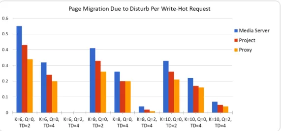
Figure 4.2: Page migration due to disturb analysis for 3 selected traces
Figure 4.3: Page migration due to disturb analysis for 3 selected traces (When TD=2)
We further investigate the performance of disturbance handling to see the reason be- hind the endurance enhancement. We calculate the number of page migrations due to disturbance per write-hot request as shown in Figure 4.2. As what we have mentioned
in Section 3.4, there are two approaches to correct a page suffering from program dis- turbance. The first approach is to rewrite again in-place, while the second approach is to migrate this data to another empty page. As you can see from Figure 4.2, increasing K, Q or TDseparately all results in a decreasing number of page migration per write-hot request. Since the page migration will invalid one page, and occupy a new empty page, it will have negative effect on the endurance of the device. Besides, we mentioned in Sec- tion 4.1 that if the reliability of the NAND flash device is lower (i.e. TD=2), increasing Q results in negative effect on the endurance. The number of page migration per write-hot request when TD=2 is shown in Figure 4.3. As you can see, increase Q results in more number of page migration. The reason is that the disturbance correction will use the first approach (i.e correct by rewrite again) more often when we increase the rewrite quota Q.
But since the device is less reliable, such correction might easily cause the disturbance to neighbor pages and thus the rewritable pages will stuck in a vicious cycle of being dis- turbed and corrected by first approach again and again. There is a counterexample when running the proxy server trace, the number of page migration due to disturb per write-hot request doesn’t increase when K=8 and 10. We found the reason behind this is that the average number of updates for all the write-hot data in the selected traces are 27, 14, and 9 respectively. Since the average update times in the proxy server is relatively small, the occurrence of program disturbance is fewer, and thus correction by in-place rewrite is ac- ceptable. We conclude that as long as the device is reliable enough (i.e. TD=4), a larger rewrite quota is more favorable to the endurance.
Chapter 5 Conclusions
In this work, we propose a disturbance-aware page rewriting, which is a programming technique for NAND flash memory. The proposed strategy allows a block to tolerate more number of write before an erase operation is needed, so it is suitable for storing write-hot data. Since it allows the device to tolerate more number of write operations per P/E cy- cle, the P/E cycle and ECC requirement can be reduced without sacrificing its endurance.
We introduce and cover its constraints by modifying the FTL components, including ad- dress translator, garbage collector, and a new disturbance handler. The experiment results shows that when using the proposed disturbance-aware page rewriting to store write-hot data, the overall endurance in the aspect of TBW can be greatly improved at most 2.21 times bettwer under fixed P/E cycle. Also, to reach the same TBW of the baseline, the P/E cycle requirement can be reduced from 1000 to at most 470, which means the ECC requirement can be reduced as well.
Bibliography
[1] Yohwan Koh. Nand flash scaling beyond 20nm. May 2009.
[2] Yu Cai, Erich F Haratsch, Onur Mutlu, and Ken Mai. Error patterns in mlc nand flash memory: Measurement, characterization, and analysis. In Proceedings of the Conference on Design, Automation and Test in Europe, pages 521–526. EDA Con- sortium, 2012.
[3] Ki-Tae Park, Myounggon Kang, Doogon Kim, Soon-Wook Hwang, Byung Yong Choi, Yeong-Taek Lee, Changhyun Kim, and Kinam Kim. A zeroing cell-to-cell interference page architecture with temporary lsb storing and parallel msb program scheme for mlc nand flash memories. IEEE Journal of Solid-State Circuits, 43(4):
919–928, 2008.
[4] Yu Cai, Onur Mutlu, Erich F Haratsch, and Ken Mai. Program interference in mlc nand flash memory: Characterization, modeling, and mitigation. In Computer De- sign (ICCD), 2013 IEEE 31st International Conference on, pages 123–130. IEEE, 2013.
[5] Alvin Cox. Solid state drive (ssd) requirements and endurance test method, 2011.
[6] Kang-Deog Suh, Byung-Hoon Suh, Young-Ho Lim, Jin-Ki Kim, Young-Joon Choi, Yong-Nam Koh, Sung-Soo Lee, Suk-Chon Kwon, Byung-Soon Choi, Jin-Sun Yum, et al. A 3.3 v 32 mb nand flash memory with incremental step pulse programming scheme. IEEE Journal of Solid-State Circuits, 30(11):1149–1156, 1995.
[7] Yu-Ming Chang, Yung-Chun Li, Ping-Hsien Lin, Hsiang-Pang Li, and Yuan-Hao Chang. Realizing erase-free slc flash memory with rewritable programming design.
In Hardware/Software Codesign and System Synthesis (CODES+ ISSS), 2016 Inter- national Conference on, pages 1–10. IEEE, 2016.
[8] Yong Sung Cho, Il Han Park, Sang Yong Yoon, Nam Hee Lee, Sang Hyun Joo, Ki-Whan Song, Kihwan Choi, Jin-Man Han, Kye Hyun Kyung, and Young-Hyun Jun. Adaptive multi-pulse program scheme based on tunneling speed classification for next generation multi-bit/cell nand flash. IEEE Journal of Solid-State Circuits, 48(4):948–959, 2013.
[9] Guiqiang Dong, Yangyang Pan, and Tong Zhang. Using lifetime-aware progressive programming to improve slc nand flash memory write endurance. IEEE Transactions on Very Large Scale Integration (VLSI) Systems, 22(6):1270–1280, 2014.
[10] Myungsuk Kim, Jaehoon Lee, Sungjin Lee, Jisung Park, and Jihong Kim. Improv- ing performance and lifetime of large-page nand storages using erase-free subpage programming. In Design Automation Conference (DAC), 2017 54th ACM/EDAC/
IEEE, pages 1–6. IEEE, 2017.
[11] Seung-Hwan Shin, Dong-Kyo Shim, Jae-Yong Jeong, Oh-Suk Kwon, Sang-Yong Yoon, Myung-Hoon Choi, Tae-Young Kim, Hyun-Wook Park, Hyun-Jun Yoon, Young-Sun Song, et al. A new 3-bit programming algorithm using slc-to-tlc migra- tion for 8mb/s high performance tlc nand flash memory. In VLSI Circuits (VLSIC), 2012 Symposium on, pages 132–133. IEEE, 2012.
[12] Yixin Luo, Yu Cai, Saugata Ghose, Jongmoo Choi, and Onur Mutlu. Warm: Improv- ing nand flash memory lifetime with write-hotness aware retention management. In Mass Storage Systems and Technologies (MSST), 2015 31st Symposium on, pages 1–14. IEEE, 2015.
[13] Tseng-Yi Chen, Yuan-Hao Chang, Chien-Chung Ho, and Shuo-Han Chen. Enabling sub-blocks erase management to boost the performance of 3d nand flash memory.
In Proceedings of the 53rd Annual Design Automation Conference, page 92. ACM, 2016.
[14] Hsin-Yu Chang, Chien-Chung Ho, Yuan-Hao Chang, Yu-Ming Chang, and Tei-Wei Kuo. How to enable software isolation and boost system performance with sub-block
erase over 3d flash memory. In Hardware/Software Codesign and System Synthesis (CODES+ ISSS), 2016 International Conference on, pages 1–10. IEEE, 2016.
[15] Guiqiang Dong, Shu Li, and Tong Zhang. Using data postcompensation and predis- tortion to tolerate cell-to-cell interference in mlc nand flash memory. IEEE Trans- actions on Circuits and Systems I: Regular Papers, 57(10):2718–2728, 2010.
[16] Jae-Duk Lee, Sung-Hoi Hur, and Jung-Dal Choi. Effects of floating-gate interference on nand flash memory cell operation. IEEE Electron Device Letters, 23(5):264–266, 2002.
[17] Ki-Tae Park, Sangwan Nam, Daehan Kim, Pansuk Kwak, Doosub Lee, Yoon-He Choi, Myung-Hoon Choi, Dong-Hun Kwak, Doo-Hyun Kim, Min-Su Kim, et al.
Three-dimensional 128 gb mlc vertical nand flash memory with 24-wl stacked layers and 50 mb/s high-speed programming. IEEE Journal of Solid-State Circuits, 50(1):
204–213, 2015.
[18] Avishay Traeger, Erez Zadok, Nikolai Joukov, and Charles P Wright. A nine year study of file system and storage benchmarking. ACM Transactions on Storage (TOS), 4(2):5, 2008.