Electric field-induced structural changes in pentacene-based organic thin-film transistors studied by in situ micro-Raman spectroscopy
H. L. Cheng,a兲W. Y. Chou, C. W. Kuo, and F. C. Tang
Institute of Electro-Optical Science and Engineering, Department of Physics, National Cheng Kung University, Tainan 701, Taiwan
Y. W. Wang
Display Technology Center, Electronics Research & Service Organization, Hsinch 310, Taiwan 共Received 20 July 2005; accepted 23 March 2006; published online 21 April 2006兲
We have investigated the electric field-induced microscopic structural changes in polycrystalline pentacene-based organic transistors by using in situ micro-Raman spectroscopy. Extra vibrational modes resulting from molecular coupling effect in pentacene film were studied. The herringbone packing of pentacene molecules in solid film is affected by external field and the process is proven to be partially irreversible. In the meantime, in-phase coupling of the C-H bending mode was found to be highly related to the carrier transport of pentacene film. Obtained results suggest that optimal intermolecular-orbital overlap of pentacene molecules is still a critical factor impacting the carrier transportation for pentacene film featuring polycrystalline morphology. © 2006 American Institute of Physics. 关DOI:10.1063/1.2197937兴
Recent technology trends draw much attention to organic thin-film transistors 共OTFTs兲. The performance of OTFTs has improved dramatically lately, and this stands true in par- ticular in regard to conjugated oligoacenes and oligothiophene.1,2 These compounds usually have polycrys- talline structure with grain morphology. Their crystalline structure is made of stacked layers wherein molecules pack in a herringbone fashion with their long axes parallel to one another. Among them, pentacene is a highly promising ma- terial for application in OTFTs due to its great mobility and good semiconducting behavior.1,2 Pentacene films with vari- ous polymorphism can be fabricated by changing the depo- sition conditions and its film structure and polymorphism both in bulk and in thin films, which have been an object of experimental and theoretical studies.3,4 However, the poly- morphism phase in pentacene film exhibits instability that can be observed by a pressure-induced5or solvent-induced6 phase transition. In addition, the OTFTs demonstrate a wide range of electrical instabilities, which affect their reliability and long-term operation capability.7,8Therefore it is impor- tant to explore the molecular structural changes during the operating cycle of OTFTs.
Micro-Raman spectroscopy is a high-resolution optical spectroscopy probe of structural and electronic properties of materials. In this letter, we focus on electric field-induced microscopic structural changes in pentacene film as an active layer in OTFTs. In situ micro-Raman spectroscopy reveal important aspects of carrier transportation and device perfor- mance at the microscopic level.
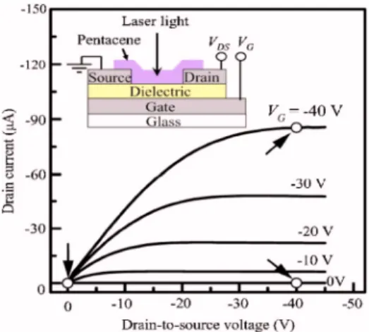
The schematic of OTFT geometry and in situ Raman measurements are shown in the inset of Fig. 1. The device geometry and the sample fabrication used in the experiments have been described previously.8–10 Indium-tin-oxide serve as the gate, source, and drain electrodes. A 3000 Å thick silicon oxide共SiO2兲 served as the gate dielectric. The penta- cene 共Aldrich Co.兲 films are vapor grown by sublimation with a thickness of 70 nm, and yielded a polycrystalline structure with only a “thin-film phase.”9The morphology of
the pentacene film was verified by x-ray diffraction spectra and an atomic force microscope.8–10The electrical character- istics of OTFTs were measured by a Keithley 4200-SCS semiconductor parameter analyzer. The electrical character- istics of pentacene OTFTs are shown in Fig. 1.
Raman spectra of pentacene films, produced by lattice phonons, were obtained using a Jobin Yvon LabRam HR spectrometer. A 532 nm solid state laser served as the exci- tation light source and was kept below 0.6 mW during mea- surements. The spatial resolution of the beam spot was around 1m, attained using a 100⫻ objective microscope lens. The spectrometer resolution is 0.4 cm−1. When the Ra- man spectra were taken, the laser beam was defocused on the surface of pentacene film to prevent thermal damage of the pentacene thin film. Every Raman spectrum was taken with an average of 20 scans. The polarized Raman spectra mea- surement and the scattering geometry was selected to be z共x,x兲z¯ or z共y,y兲z¯, where the first symbol stands for the di- rection of propagation of the incident laser beam; the terms in parentheses specify the polarization of the incident beam and that of the scattered radiation, respectively, while the final symbol represents the direction of propagation of the scattered radiation.
a兲Electronic mail: [email protected]
FIG. 1. The output characteristics of the pentacene OTFTs共channel length
=60m, channel width =10 mm兲. Inset: Schematic of the pentacene OTFT and the in situ micro-Raman measurement setup.
APPLIED PHYSICS LETTERS 88, 161918共2006兲
0003-6951/2006/88共16兲/161918/3/$23.00 88, 161918-1 © 2006 American Institute of Physics
Downloaded 20 Jul 2009 to 140.116.208.56. Redistribution subject to AIP license or copyright; see http://apl.aip.org/apl/copyright.jsp
The pentacene thin films have a layered structure4and a calculated interlayer d001 spacing of 15.4 Å of thin-film phase, which is slightly lower than the length of the penta- cene molecule; thus the molecules are slightly tilted to the substrate plane. The interlayer structure of pentacene film depends on the relative multitude of C-H and C-C interac- tions. If the C-H interactions dominate, a herringbone struc- ture is generally found.4 In this analysis, we focus on the C-H in-plane bending of pentacene molecule in the energy range of 1140– 1200 cm−1, which shows that the strongest motions of the atoms are recorded at the end of the molecule.
Figure 2共a兲 shows the Raman spectrum of pentacene OT- FTs before operation. The main bands at 1158 and 1178 cm−1correspond to origin from the C-H in-plane mo- lecular vibration of each pentacene molecule. A Gaussian/
Lorentzian function fitting procedure for finding the best fit- ting, performed in the range falling between 1140 and 1170 cm−1, reveals that the feature at⬃1158 cm−1共denoted as the v0 band兲 actually consists of three lines centered at
1154.5 共denoted as the v1 band兲, 1158.3, and 1162.7 cm−1 共denoted as the v2 band兲. The fitting results are shown in Table I. The splitting atv1 共Ref. 11兲 and v2 共Ref. 12兲 bands have been explained by the different interaction energy be- tween the two adjacent pentacene molecules in a unit cell at different angular positions, analogous to Davydov splitting.11 However, the origin of difference between v1and v2 bands remained unclear. Later in this letter we will discuss the pos- sible origins ofv1andv2bands.
Initially, we studied the effects of gate bias 共VG兲 关Fig.
2共b兲, VG= −40 V兴 and drain bias 共VDS兲 关Fig. 2共c兲, VDS=
−40 V兴 on pentacene molecules using in situ Raman spec- troscopy. The negative VGand VDSall induced the frequency downshift of the peak center and an increased Raman inten- sity. As seen in Table I, the negative VG induced a larger change on thev0 band than on bandsv1 andv2. Obviously, an extra dipole moment induced by the gate field had a great influence on the pentacene in-plane v0 band along the long axis 共c-axis兲 of the pentacene molecule. The gate field of 106V cm−1 共at VG= −40 V兲 induced a larger spectral area increase as compared to the drain field of 104V cm−1共at VDS= −40 V兲. The drain field, however, induced a larger fre- quency downshift of 0.8– 1.1 cm−1 versus the gate field ef- fect of 0.3– 0.6 cm−1. Especially, thev1band shows a larger change in the Raman spectral area increase in comparison with other modes.
Next, we turn our attention to the in situ Raman spec- trum during the device operation in the saturation regime at VG= VDS= −40 V 关Fig. 2共d兲兴. We can observe a more pro- nouncedv1 band共by a factor of 1.81兲. The v1andv2 bands show a larger increment in the spectral peak area than do the v0 bands. In particular, we can see the proof in the band 1178 cm−1 splitting into two modes and shifting to lower frequencies at 1176 and 1177 cm−1. Such splitting at 1178 cm−1 has been recorded in the presence of polymorph phases in the film13as well as a pressure-induced irreversible phase transition in the bulk-phase pentacene.5
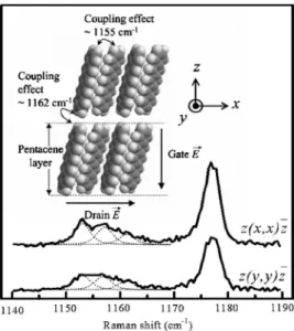
To further realize the coupling effect between the penta- cene molecules under the drain field, we have tracked the C-H modes by in situ polarized Raman spectra共Fig. 3兲. The
FIG. 2. Raman spectra of pentacene taken in situ during the operations of OTFTs:共a兲 Before operations, 共b兲 only at VG= −40 V,共c兲 only at VDS=
−40 V,共d兲 at VG= VDS= −40 V. The Gaussian/Lorentzian functions used for the deconvolution are shown as a dotted line. Thev0,v1, andv2bands were assigned in the text and dashed lines serve as guidelines. Note: Spectra 共a兲–共d兲 from different devices on the same substrate within 1.5 cm2. For deposited pentacene films on the same substrates, the Raman spectra are substantially the same.
TABLE I. The fitting results of the C-H bending modes of pentacene film in OTFTs.max= Raman shift of peak center, Arel= the relative spectra area, Av1/ Av0ratio⫽ the spectral area ratio of v1band tov0band, and Av2/ Av0 ratio⫽ the spectral area of v2band tov0band. The standard errors of the spectral area ratio are within 6%.
v0band v1band v2band
max Arela max Arela max Arela Av
1/ Av
0 Av
2/ Av
0
Sample and measurement
conditions 共cm−1兲 共cm−1兲 共cm−1兲 ratio ratio
Before operations 1158.3 1.00 1154.5 1.00 1162.7 1.00 0.65 0.67
Gate bias effect共VG= −40 V兲 1157.7 1.49 1154.2 1.41 1162.2 1.35 0.61 0.60 Drain bias effect共VDS= −40 V兲 1157.5 1.18 1153.6 1.36 1161.6 1.16 0.75 0.66 Operated at VG= VDS= −40 V 1157.8 1.29 1154.1 1.81 1161.8 1.42 0.91 0.74 Drain bias effect共VDS= −40 V兲
polarization z共x,x兲z¯ 共Fig. 3兲 1157.4 1.39 1153.5 1.54 1161.3 1.25 1.17 0.59 polarization z共y,y兲z¯ 共Fig. 3兲 1157.0 — 1153.4 — 1161.2 — 1.06 0.66 On PAPI, fresh sampleb
polarization z共x,x兲z¯ 1158.4 1.67 1154.3 2.08 1162.1 1.49 1.56 0.53
polarization z共y,y兲z¯ 1157.8 — 1154.3 — 1161.7 — 1.24 0.59
aData from Fig. 2 represents the increment compared to a fresh sample. Data measured at a different polariza- tion geometry indicates the spectral area ratio of z共x,x兲z¯ to z共y,y兲z¯ geometry.
bPentacene film was grown on a PAPI surface; see the details of experiments in Refs. 9 and 15. Data is taken from Fig. 5 in Ref. 15.
161918-2 Cheng et al. Appl. Phys. Lett. 88, 161918共2006兲
Downloaded 20 Jul 2009 to 140.116.208.56. Redistribution subject to AIP license or copyright; see http://apl.aip.org/apl/copyright.jsp
scattering geometries employed were z共x,x兲z¯ and z共y,y兲z¯, where the labels x, y, and z refer to being parallel to source- to-drain, perpendicular to source-to-drain, and perpendicular to substrate plane directions, respectively. The Gaussian/
Lorentzian fitting results are also shown in Table I. In z共x,x兲z¯
geometry, all C-H bending modes display a stronger inten- sity than in z共y,y兲z¯ geometry. This is especially notable at thev1band, with its peak area being about 1.54 times more as compared to the z共y,y兲z¯ geometry. A larger intensity of thev1 band implies the presence of a strong interaction be- tween the pentacene molecules along the direction of the drain field共see the inset of Fig. 3兲. Consequently, the v1band is attributed to the in-phase coupling between the pentacene molecules. As compared to thev1band, a decreased intensity of the v2 band under the drain field can be interpreted as out-of-phase coupling between the different layers of the pentacene molecules 共see the inset of Fig. 3兲. This conclu- sion is also supported by the monolayer pentacene films, which have not seen thev2 band,13 and the insertion of io- dine between pentacene layers that is also affecting the band.12
Our studies demonstrate clear evidence on the structural changes of pentacene in the operating OTFT device. The structural changes in the pentacene were found to be partially irreversible after operations were repeated many times. After multiple operation cycles, we could observe a more pro- nounced v1 band and shifts to ⬃1153 cm−1. Even without application of the electric field, the ⬃1153 cm−1 band re- mains strong and differs from that observed in a fresh sample. Obviously, the molecular geometry changes of pen- tacene cannot recover to their initial state.
At the microscopic level, the intermolecular coupling ef- fect共optimal-orbital overlap兲 should be maximized to en- sure efficient carrier transport.14We once again examined the pentacene film, with morphology and orientation different from that found in previous studies, by applying the photo-
alignment polyimide共PAPI兲 method.9,15The results are also shown in Table I. Interestingly, the pentacene shows a stron- gerv1band at polarization z共x,x兲z¯ geometry as compared to z共y,y兲z¯ geometry when the pentacene is aligned along the direction of source to drain, with the corresponding field- effect mobility of 0.82 and 0.15 cm2/ V s at z共x,x兲z¯ and z共y,y兲z¯ geometry, respectively. Compared to the pentacene film deposited onto the untreated SiO2, the mobility was only 0.08 cm2/ V s and the corresponding spectral area ratio ofv1 band to v0 band 共Av1/ Av
0兲 was 0.65. These results provide the basis for understanding and control of the carrier trans- port efficiency in a polycrystalline pentacene film in the con- text of microscopic molecular structure.
To summarize, we should reinforce once again that mo- lecular geometry changes of pentacene in an operating OTFT device were studied by applying a gate and drain field com- bined with in situ Raman spectroscopy. It was found that it is possible to assign extra vibrational modes from the molecu- lar coupling effect of the polycrystalline pentacene solid film by applying the aforementioned field. The in-phase coupling of the C-H bending mode between pentacene molecules within the monolayer was enhanced by a parallel drain-to- source field. The results suggest that the in-phase coupling 共v1mode兲 is highly related to the carrier transport of a pen- tacene thin film. Based on the research, it is obvious that structural changes should be further investigated in order to understand charge carrier motions in a pentacene thin film.
The authors acknowledge financial support from the Na- tional Science Council, Taiwan, through Grant NSC 93- 2215-E-006-039 and NSC 93-2112-M-006-004. The assis- tance of the Center for Micro/Nano Technology Research, National Cheng Kung University, for support through equip- ment and cooperation is gratefully acknowledged.
1C. D. Dimitrakopoulos and P. R. L. Malenfant, Adv. Mater.共Weinheim, Ger.兲 14, 99 共2002兲.
2T. W. Kelley, D. V. Muyres, P. F. Baude, T. P. Smith, and T. D. Jones, Mater. Res. Soc. Symp. Proc., 771, 169共2003兲.
3R. G. Della Valle, A. Brillante, E. Venuti, L. Farina, A. Girlando, and M.
Masino, Org. Electron. 5, 1共2005兲, and references therein.
4C. C. Mattheus, G. A. de Wijs, R. A. de Groot, and T. T. M. Palstra, J. Am.
Chem. Soc. 125, 6323共2003兲, and references therein.
5A. Brillante, R. G. Della Valle, L. Farina, A. Girlando, M. Masino, and E.
Venuti, Chem. Phys. Lett. 375, 490共2003兲.
6D. J. Gundlach, T. N. Jackson, D. G. Schlom, and S. F. Nelson, Appl.
Phys. Lett. 74, 3302共1999兲.
7D. Knipp, R. A. Street, A. Völkel, and J. Ho, J. Appl. Phys. 93, 347 共2003兲, and references therein.
8Y. W. Wang, H. L. Cheng, Y. K. Wang, T. H. Hu, J. C. Ho, C. C. Lee, T.
F. Lei, and C. F. Yeh, Thin Solid Films 467, 215共2004兲, and references therein.
9W. Y. Chou and H. L. Cheng, Adv. Funct. Mater. 14, 811共2004兲.
10Y. W. Wang, H. L. Cheng, Y. K. Wang, T. H. Hu, J. C. Ho, C. C. Lee, T.
F. Lei, and C. F. Yeh, Thin Solid Films 491, 305共2005兲.
11T. Jentzsch, H. J. Juepner, K. W. Brzezinka, and A. Lau, Thin Solid Films 315, 273共1998兲.
12M. Cazayous, A. Sacuto, G. Horowitz, Ph. Lang, A. Zimmers, and R. P. S.
M. Lobo, Phys. Rev. B 70, 081309共R兲 共2004兲.
13R. He, I. Dujovne, L. Chen, Q. Miao, C. F. Hirjibehedin, A. Pinczuk, C.
Nuckolls, C. Kloc, and A. Ron, Appl. Phys. Lett. 84, 987共2004兲.
14V. Coropceanu, M. Malagoli, D. A. da Silva Filho, N. E. Gruhn, T. G. Bill, and J. L. Brédas, Phys. Rev. Lett. 89, 275503共2002兲.
15W. Y. Chou, C. W. Kuo, Y. S. Mai, S. T. Lin, H. L. Cheng, C. C. Liao, and D. Y. Shu, Proc. SPIE 5522, 97共2004兲.
FIG. 3. Raman spectra of pentacene, measured at two polarization condi- tions, taken in situ during the operations of OTFTs only at VDS= −40 V. The Gaussian/Lorentzian functions used for the deconvolution are shown as a dotted line. The dashed lines serves as guidelines. The inset schematic dis- plays the coupling effect of pentacene molecules between and within the layered structure under gate and drain field.
161918-3 Cheng et al. Appl. Phys. Lett. 88, 161918共2006兲
Downloaded 20 Jul 2009 to 140.116.208.56. Redistribution subject to AIP license or copyright; see http://apl.aip.org/apl/copyright.jsp