Fu-Hai Li, Student Member, IEEE, Nina Mitiukhina, and Hideki Arakawa, Member, IEEE
Abstract—This paper investigates the new programming
scheme to reduce the program disturb in theNANDFlash memory. Program disturb characteristics are determined by the unwilling electron injections in the floating gate of the unselected cells during programming. Thus, the key point to improve the program disturb characteristics is how to suppress the electron injection in the unselected cells. This requirement can be implemented by reducing the number of electrons in the unselectedNANDstrings prior to programming. By applying negative bias to all the word lines in the selected block, excess electrons can be removed from the channel and source/drain regions into the bit line or the source line using drift and diffusion mechanisms, and also electrons in the surface states can be recombined with accumulated holes before programming. After the pretreatment of electron reduction in theNAND string, a normalNAND program sequence follows. The advantage of the pretreatment before programming has been verified by measuring the 8-GbNANDFlash memory with a 50-nm technology node. Significant reduction of the threshold voltage shift was observed even after the severe program disturb stress, which corresponds to around 30 times of the programming of the 2 bit/cell operation.
Index Terms—Flash memory, Fowler–Nordheim (FN)
tunnel-ing, junction leakage (J/L),NANDcell, program disturb, select gate (SG), surface state.
I. INTRODUCTION
T
HROUGH A decade,NANDscaling has been in progress from 250- to 25-nm technology nodes [1], [2], and re-cently, the design rule has already reached 20 nm and has continued further [3]–[7]. However, as the cell size is scaled, Vt shift according to the parasitic neighboring cell coupling has become more and more serious. In addition, Vt distribution due to the Fowler-Nordheim-tunneling statistics and random telegraph noise also has become more severe [8], [9]. Therefore,Manuscript received March 22, 2012; revised May 23, 2012 and June 26, 2012; accepted July 3, 2012. Date of publication August 24, 2012; date of current version September 18, 2012. The review of this paper was arranged by Editor Y.-H. Shih.
R. Shirota, F.-H. Li, and N. Mitiukhina are with the Department of Elec-trical and Computer Engineering, Institute of Communications Engineering, National Chiao Tung University, Hsinchu 300, Taiwan (e-mail: rshirota@ faculty.nctu.edu.tw; [email protected]; [email protected]).
C.-H. Huang, Y. Sakamoto, and H. Arakawa are with the Powerchip Tech-nology Corporation, Hsinchu 300, Taiwan (e-mail: [email protected]; [email protected]; [email protected]).
S. Nagai is with the PowerMemory Corporation, Tokyo 105-0004, Japan (e-mail: [email protected]).
Color versions of one or more of the figures in this paper are available online at http://ieeexplore.ieee.org.
Digital Object Identifier 10.1109/TED.2012.2208462
there has been no room for the Vt variation due to program disturb. The program disturb is one of the key issues to be overcome for the NAND-cell scaling. The channel boosting potential degradation due to small channel boosting ratio (CBR) and electron generations by junction leakage (J/L) limits the program disturb [10]. The gate-induced drain leakage (GIDL) at the select gate (SG) also has been reported to degrade the channel boosting voltage [11]. These disturb issues become more serious as the cell scales down and the channel boron con-centration increases. Many approaches have been discussed to improve theNAND-cell program disturb. Source/drain junction engineering has been pursued to improve the J/L [12]–[14]. A local self-boost scheme was proposed to improve the CBR [15]. A dummy word line (WL) structure was suggested to overcome the GIDL problem at the SG-WL space [16]. However, the program disturb issues due to the insufficient channel boosting remain as one of the main concerns for the NAND-cell scaling [17]. In this paper, we propose a new programming disturb-free scheme (PDFS) to improve the program disturb characteristics by increasing the boosted channel potential [18]. The key to increase the channel potential is to eliminate the electrons in the channel before programming.
Furthermore, PDFS also makes it possible to divide one page into small sectors for programming (partial page programming) even in the case of MLC operation. This paper is arranged by firstly introducing the new programming scheme to suppress the program disturb. Next, the effect of the proposed operation is demonstrated with the experimental results by using an 8-Gb MLC NANDFlash memory with a 50-nm design rule, and the physical analysis is performed using 3-D device simulations.
II. ISSUES OFCONVENTIONALSELF-BOOSTOPERATION
Conventionally, the self-boosting operations [10]–[17] are tested while they cannot fully prevent the program disturb. For instance, consider the case that memory cells in the string are all in erased state. The timing diagram is shown in Fig. 1, where VSGD is set to be higher than Vt(SGD) to pass the 0 V in the selectedNANDcell string and VBL is set to be higher than VSGD-Vt(SDG) to cut off the SG transistor of the unselected
NANDcell string for program inhibition. Before programming (t < t1), positive biases are applied both to the bit lines (BLs) and BL side SGs (SGDs) in order to eliminate electrons inside aNANDstring.
Fig. 1. Timing diagram of conventional program scheme for BL, drain side SG, and selected and unselected WL biases.
Fig. 2. Lateral band diagram and carrier distribution in the conventional scheme at the inhibit cell string during t1< t < t2, where the carriers
re-mained in every channel region, under the condition:|Vt(cell)| − VSGD − Vt(SGD), where SGD means BL side SG.
However, when erased Vt is deep enough [|Vt(cell)| > VSGD− Vt(SGD)], a large amount of electrons still remain in the whole channel region before programming, as shown in Fig. 2. During programming (t2 < t < t3), Vpass pulses are applied to the unselected WLs, and Vprg (Vprg > Vpass) is applied to the selected WL. Some electrons from the NAND
string are laterally transferred into the channel of the program-inhibit cell under the selected WL, and this leads to the lowering of the surface potential of this cell, which will cause program disturb, as shown in Fig. 3. Higher Vpass can improve the program disturb issue. However, it causes the Vt shift of the cells in the strings with VBL = 0 V. When the local self-boosting scheme is used, the boosted channel potential can be higher than the potential of the self-boosting one. However, even at the conventional local self-boosting scheme, the re-maining electrons in the string can be injected into FG due to the energetic acceleration by high electric field in the deep depletion region in the channel.
III. NEWPROGRAMBIASINGSCHEME
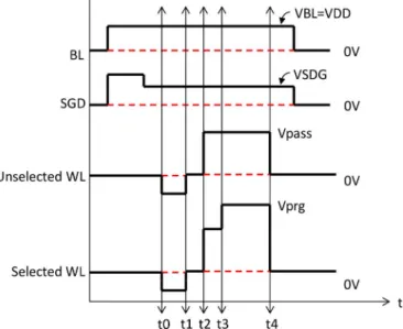
The proposed new scheme includes a step of applying a neg-ative bias to all WLs in a selected block before programming, as shown in Fig. 4. Positive biases are applied to the SGD and BL, and a negative bias is applied to all WLs at the time t0 < t < t1.
scheme during t2 < t < t3, where the electrons are concentrated in the chan-nel under selected WL. Electron injection will easily occur due to the low surface potential in the cell with VWL = Vprg.
Fig. 4. Timing diagram of proposed method for BL, drain side SG (SGD), and selected and unselected WL biases.
Fig. 5. Lateral band diagram and carrier distribution in the proposed scheme during t0 < t < t1, where the hole accumulation layer is formed in the channel and the ionizations of the interface traps are taking place.
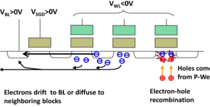
During this period, several phenomena occur at the same time, to reduce the number of excess electrons in the NAND cell string. First, the negative WLs induce the hole accumulation at the surface of every channel region. Then, excess electrons in the channel and S/D drift to BL or diffuse into SL and neighboring blocks, as shown in Figs. 5 and 6. Moreover, some of the electrons trapped at the oxide interface will be detrapped and also drift and/or diffuse into BL, SL, and neighboring blocks. Furthermore, these accumulated holes will ionize the donor-type capture centers, e.g., the surface states. Moreover,
Fig. 6. Mechanism to reduce the amount of electrons in the cell string: 1) By applying negative bias to WLs, electrons in the conduction band drift to the BL or diffuse to the source line, and 2) some of the accumulated holes in the Si surface recombine with electrons in the surface state.
Fig. 7. Band diagram and carrier distribution in the proposed scheme. During
t0 < t < t1, negative bias is applied to WLs. First, electrons in the surface
state are recombined with accumulated holes. Second, the excess electrons in the conduction band are removed from the surface.
Fig. 8. Lateral band diagram and carrier distribution in the proposed scheme during t3 < t < t4, where the number of electrons in the channel under selected WL is significantly reduced and Si surface potential becomes high.
at the same time, electrons captured by the surface states recombine with the accumulated holes, as shown in Figs. 6 and 7. As a result, the electron density in theNANDcell string becomes very low. Then, Vprg and Vpass are applied to WLs, following the conventional sequence at the time t2 < t < t4. The surface potential of the inhibit cell can be maintained at the high level because of the aforementioned excess electron elimination, as shown in Fig. 8. As a result, the program disturb is effectively prevented. During the actual programming period (t2 < t < t4), the self-boosting method is used to examine the
Fig. 9. (a) Vt distribution of “01” state (lowest level in three states) before and after program disturb stresses of 100, 200, and 500 pulses. Vprg is 22 V. Data of two program schemes (conventional self-boost and PDFS) are compared. Inset shows the typical programming characteristics of the cell. (b) Vt distribution of “01” state (lowest level in three states) before and after program disturb stress of 500 pulses. Vprg is 22 V. Data of three program schemes (conventional self-boost, conventional local self-self-boost, and PDFS) are compared. (c) Comparison of Vt shift of Vt distribution at three different program schemes. Vt shifts of the Vt distribution (+3σ) before and after stress are shown.
extent of the improvement of program disturb, which is shown in the next section. However, local self-boosting scheme is also available to use.
IV. EXPERIMENT ANDSIMULATIONRESULTS
The proposed program scheme is verified with the experi-ment using the 8-Gb Flash memory and miniarray of theNAND
strings (test key device), where 50-nm design rules are used. The number of the cells in the NAND string is 32. Fig. 9(a) shows the Vt distribution in one page (2 KB) before and after applying program pulses 500 times, where Vprg is fixed at 22 V (monitoring Vt of the cells in the program-inhibit state). Initially, the cells in one page are programmed to “01” states (Vt ≥ 0.4 V). The other cells in the NAND cell string
Fig. 10. Vt shift of the Vt distribution at −3σ for “C” level case after applying the negative WL bias stress, which corresponds to 32 times of partial programming stress in each page for the case of 2 bit/cell programming.
(31 cells) are all in erased state. We compared the program disturb characteristics of the conventional self-boosting and the new PDFS scheme. The conventional self-boosting scheme shows large Vt shift after applying program stress 500 times. For example, Vt (monitored at 3σ of the Vt distribution) shifts from 1 V (initial) to 2.4 V (after stress). On the other hand, by using the PDFS scheme, few Vt shifts are observed at the inhibit cells even after applying Vprg stress 500 times (applying 22 V to the selected WL 500 times roughly corresponds to 30 times of the partial page programming of the 2 bit/cell mode). There-fore, PDFS enables the sector programming which divides one page to the small sectors, and each of them can be indepen-dently programmed, even at the case of MLC operation. The sector programming will be useful to improve the reliability of theNANDFlash. Fig. 9(b) shows the program disturb char-acteristics using three different schemes after applying Vprg stress 500 times, where Vprg is 22 V. Fig. 9(c) compares the Vt shift (3σ of the Vt distribution) of three different program schemes as a function of the number of program pulses. The conventional local self-boosting scheme shows smaller Vt shift than in the case of the conventional self-boosting method; however, significant Vt shift still exists after applying Vprg stress 500 times. On the other hand, PDFS exhibits virtually no Vt shift under similar conditions. Fig. 9(a)–(c) indicates that the elimination of electrons in theNANDcell string before programming can strongly prohibit the electron injections into FG at the program-inhibit cell.
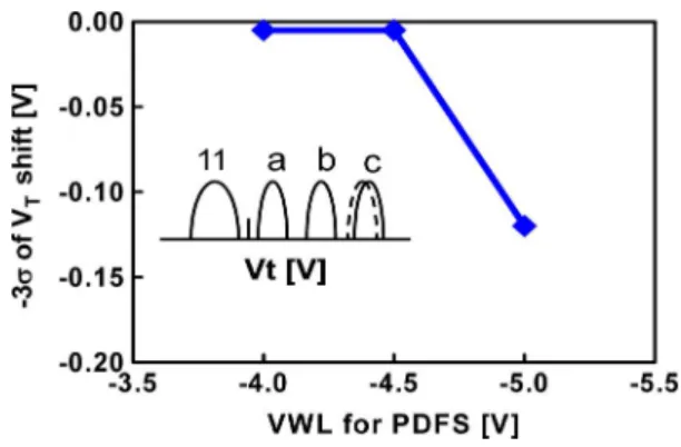
Fig. 10 shows the Vt distribution after applying the negative WL stress to one block. The stress time can be calculated as 32 (partial page programming times) × average number of programming pulses× number of pages per block × program pulse width = 32× 12 × 128 × 20 μs ∼ 0.98 sec. The Vt shift of the highest state (“C” level) is almost negligible when the negative WL bias is higher than −4.5 V. Thus, even when we are in partial page programming mode, which divides one page to small sectors, the Vt of the “C” level cells will have immunity against the negative WL stress. Fig. 11 shows the Vpass dependence of program disturb by using a miniarray test key device. The conventional self-boosting scheme has a small Vpass margin. When Vpass is lower than 8 V, the channel boosting level is not high enough, and the program disturb happens. On the other hand, Vpass voltage cannot be too high in order to prohibit the Vt shift at the cells with VBL = 0 V and
Fig. 11. Program disturbance characteristics as a function of Vpass voltage, where Vprg is 22 V. Conventional self-boost and PDFS program schemes (followed by self-boost programming) are compared. PDFS shows good char-acteristics almost independent of Vpass. 32 cells are connected in series in the
NANDcell string.
Fig. 12. +3σ of Vt distribution as a function of negative WL bias before programming. Initially, cells are in erased state. Vprg is 22 V. Program pulses are applied 500 times.
VWL = Vpass. In the case of the PDFS scheme, the program disturb can be highly suppressed even though the Vpass is essentially lowered, particularly for the levels less than 5 V, which are showing the excellent performance. Therefore, the PDFS scheme is able to significantly enlarge the Vpass margin. The new scheme is also effective for an edge WL (WL0 and WL31) without suffering GIDL, when the distance from SG to WL and the S/D dose are properly optimized. Fig. 12 shows the program disturb characteristics as a function of the negative WL bias applied before programming in PDFS. The pulsewidth of the negative WL is set to 5 s, which will give a small impact on the programming time. The improvement of program disturb by PDFS takes place when negative WL bias is lower than
−3 V. Fig. 13 shows the negative WL pulsewidth dependence of
the 3σ of the Vt distribution at the “11” state. The elimination of the excess electrons in theNAND cell string is almost done within 5 μs, as shown in Fig. 13. Fig. 14 shows the program disturb characteristics as a function of the program WL voltage (Vprg) at the PDFS scheme. It is shown that the PDFS scheme is effective in the wide range of Vprg form 20 to 23 V, where 22 V is usually the maximum voltage at the 2 bit/cell programming.
Fig. 15 shows the data pattern dependence of neighboring cells in theNANDstring at the PDFS scheme. In order to clear the data pattern dependence, Vprg is set to be as high as 23 V. However, the Vt shift of the program-inhibit cell shows small dependence on the data pattern. The PDFS scheme provides the
Fig. 13. +3σ of Vt distribution at “11” state as a function of pulsewidth of the negative WL.
Fig. 14. Vt shift of Vt distribution at +3σ is shown as a function of Vprg voltage. Initially, cells are in “01” state. Program pulses are applied 500 times.
Fig. 15. Vt shift of Vt distribution at +3σ is shown to be dependent on data pattern (using PDFS). Initially, cells in WLn are in “01” states. Next, cells in WLn suffered program-inhibit stress (Vprg is 23 V, and program pulses are applied 500 times). Data patterns in the neighboring cells in the cell string are different. The neighboring cells are preprogrammed, before programming WLn. 3σ of Vt shift at conventional scheme is more than 2.2 V even in all erased state.
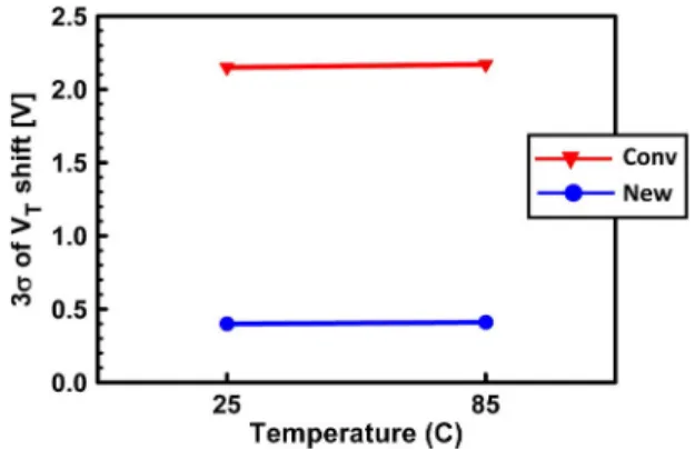
wide margin of program operation even encountering the worse data pattern (when neighboring cells in the cell string are pro-grammed to high Vt before programming selected WLn). The surface potentials of the neighboring cells (WLn-1, WLn+1) in theNANDstring are lower than the potential of WLn’s, which forms some barrier for electrons to drift or diffuse to BL and SL during applying negative bias to all WLs. However, from Fig. 15, it is clear that the effect of elimination of electrons in the string is valid even in case of these data patterns. Fig. 16 shows the temperature dependence of the conventional and PDFS schemes. Small temperature dependence is observed in the wide range from 25◦C to 85 ◦C. Finally, Fig. 17 shows
Fig. 16. Temperature dependence of the program disturb is shown. Conven-tional self-boosting and PDFS schemes are compared. Almost no temperature dependence is observed in both cases.
Fig. 17. Three-dimensional T-CAD simulation results of Si surface potential during applying Vprg and Vpass to WLs. Vprg is set 20 V. In this simulation, four cells + two SGs are arrayed in series. The difference of the surface potential between three schemes come from the difference in the amount of electrons in theNANDstring.
the 3-D device simulation results of the surface potential in comparison with the conventional program scheme. For the conventional program scheme, both self-boosting and local self-boosting cases are shown. The PDFS scheme attains the highest surface potential of the inhibit cell while programming, where self-boosting scheme is used in the period between
t2 < t < t4 for the convenience. Local self-boosting is also
applicable to use in the period between t2 < t < t4. Generally, the tunneling current (J) is expressed by the multiplex of the tunneling probability (P) times the electron density of the Si surface (N) as J = P × N. The tunneling probability P is the function of the voltage difference between FG and channel potential [VFG - V(channel)]. Thus, there are two reasons of the improvement of the program disturb characteristics at the PDFS scheme. One is that the highest boosting potential of the channel reduces the tunneling probability P. The other comes from the decreased surface electron density N at the program-inhibit cells for the PDFS scheme.
V. CONCLUSION
The proposed scheme is successfully demonstrated as the most effective method to prevent the program disturbance,
ACKNOWLEDGMENT
The authors would like to thank A. Wu and all members of the RD business group in Powerchip Technology Corporation for the fabrication and supports of characterization.
REFERENCES
[1] R. Shirota, “A review of 256 Mbit NAND flash memories and NAND flash future trend,” in Proc. Non-Volatile Semicond. Memory Workshop, 2000, pp. 22–32.
[2] T. Kamigaichi, F. Arai, H. Nitsuta, M. Endo, K. Nishihara, T. Murata, H. Takekida, T. Izumi, K. Uchida, T. Maruyama, I. Kawabata, Y. Suyama, A. Sato, K. Ueno, H. Takeshita, Y. Joko, S. Watanabe, Y. Liu, H. Meguro, A. Kajita, Y. Ozawa, T. Watanabe, S. Sato, H. Tomiie, Y. Kanamaru, R. Shoji, C. H. Lai, M. Nakamichi, K. Oowada, T. Ishigaki, G. Hemink, D. Dutta, Y. Dong, C. Chen, G. Liang, M. Higashitani, and J. Lutze, “Floating gate super multilevel NAND Flash memory technology for 30 nm and beyond,” in IEDM Tech. Dig., 2008, pp. 827–830.
[3] K. Prall and K. Parat, “25 nm 64 Gb MLC NAND technology and scaling challenges,” in IEDM Tech. Dig., 2010, pp. 102–105.
[4] C. H. Lee, S. K. Sung, D. J. S. Lee, S. Choi, J. Kim, S. Park, M. Song, H. C. Baek, E. Ahn, J. Shin, K. Shin, K. Min, S. S. Cho, C. J. Kang, J. Choi, K. Kim, J. H. Choi, K. D. Suh, and T. S. Jung, “A highly manufacturable integration technology for 27 nm 2 and 3 bit/cell NAND flash memory,” in IEDM Tech. Dig., 2010, pp. 98–101.
[5] K. Fukuda, Y. Watanabe, E. Makino, K. Kawakami, J. Sato, T. Takagiwa, N. Kanagawa, H. Shiga, N. Tokiwa, Y. Shindo, T. Edahiro, T. Ogawa, M. Iwai, O. Nagao, J. Musha, T. Minamoto, K. Yanagidaira, Y. Suzuki, D. Nakamura, Y. Hosomura, H. Komai, Y. Furuta, M. Muramoto, R. Tanaka, G. Shikata, A. Yuminaka, K. Sakurai, M. Sakai, H. Ding, M. Watanabe, Y. Kato, T. Miwa, A. Mak, M. Nakamichi, G. Hemink, D. Lee, M. Higashitani, B. Murphy, B. Lei, Y. Matsunaga, K. Naruke, and T. Hara, “A 151 mm2 64 Gb MLC NAND flash memory in 24 nm CMOS technology,” in ISSCC Dig. Tech. Papers, 2011, pp. 198–199.
[6] K. T. Park, O. Kwon, S. Yoon, M. H. Choi, I. M. Kim, B. G. Kim, M. S. Kim, Y. H. Choi, S. H. Shin, Y. Song, J. Y. Park, J. E. Lee, C. G. Eun, H. C. Lee, H. J. Kim, J. H. Lee, J. Y. Kim, T. M. Kweon, H. J. Yoon, T. Kim, D. K. Shim, J. Sel, J. Y. Shin, P. Kwak, J. M. Han, K. S. Kim, S. Lee, Y. H. Lim, and T. S. Jung, “A 7 MB/s 64 Gb 3-bit/cell DDR NAND flash memory in 20 nm-node technology,” in ISSCC Dig.
Tech. Papers, 2011, pp. 212–213.
[7] T. Y. Kim, S. D. Lee, J. S. Park, H. Y. Cho, B. S. You, K. H. Baek, J. H. Lee, C. W. Yang, M. Yun, M. S. Kim, J. W. Kim, E. S. Jang, H. Chung, S. O. Lim, B. S. Han, and Y. H. Koh, “A 32 Gb MLC NAND flash memory with Vth margin-expanding schemes in 26 nm CMOS,” in
ISSCC Dig. Tech. Papers, 2011, pp. 202–203.
[8] R. Shirota, Y. Sakamoto, H. M. Hsueh, J. M. Jaw, W. C. Chao, C. M. Chao, S. F. Yang, and H. Arakawa, “Analysis of the correlation between the programmed threshold-voltage distribution spread of NAND Flash memory devices and floating-gate impurity concentration,” IEEE
Trans. Electron Devices, vol. 58, no. 11, pp. 3712–3919, Nov. 2011.
[9] A. Ghetti, C. M. Compagnoni, F. Biancardi, A. L. Lacaita, S. Beltrami, L. Chiavarone, A. S. Spinelli, and A. Visconti, “Scaling trends for random telegraph noise in deca-nanometer Flash memories,” in IEDM Tech. Dig., 2008, pp. 835–838.
[10] S. Satoh, H. Hagiwara, T. Tanzawa, K. Takeuchi, and R. Shirota, “A novel isolation-scaling technology for NAND EEPROMs with the minimized program disturbance,” in IEDM Tech. Dig., 1997, pp. 291–294. [11] J. D. Lee, C. K. Lee, M. E. Lee, H. S. Kim, K. C. Park, and W. S. Lee,
“A new programming disturbance phenomenon in NAND flash memory
in IEDM Tech. Dig., 1999, pp. 271–274.
[15] T. S. Jung, Y. J. Choi, K. D. Suh, B. H. Suh, J. K. Kim, Y. H. Lim, Y. N. Koh, J. W. Park, K. J. Lee, J. H. Park, K. T. Park, J. R. Kim, J. H. Yi, and H. K. Lim, “A 117-mm2 3.3-V only 128-Mb multilevel NAND flash memory for mass storage applications,” IEEE J. Solid-State
Circuits, vol. 31, no. 11, pp. 1575–1583, Nov. 1996.
[16] K. Kanda, M. Koyanagi, T. Yamamura, K. Hosono, M. Yoshihara, T. Miwa, Y. Kato, A. Mak, S. L. Chan, F. Tsai, R. Cernea, B. Le, E. Makiko, T. Taira, H. Otake, N. Kajimura, S. Fujimura, Y. Takeuchi, M. Itoh, M. Shirakawa, D. Nakamura, Y. Suzuki, Y. Okukawa, M. Kojima, K. Yoneya, T. Arizono, T. Hisada, S. Miyamoto, M. Noguchi, T. Yaegashi, M. Higashitani, F. Ito, T. Kamei, G. Hemink, T. Maruyama, K. Ino, and S. Ohshima, “A 120 mm2 16 Gb 4-MLC NAND flash memory with 43 nm CMOS technology,” in ISSCC Dig. Tech. Papers, 2008, pp. 430–431.
[17] A. Torsi, Y. Zhao, H. Liu, T. Tanzawa, A. Goda, P. Kalavade, and K. Parat, “A program disturb model and channel leakage current study for sub-20 nm NAND Flash cells,” IEEE Trans. Electron Devices, vol. 58, no. 1, pp. 11–15, Jan. 2011.
[18] R. Shirota, C. H. Huang, and H. Arakawa, “A new disturb free program-ming scheme in scaled NAND flash memory,” in IEDM Tech. Dig., 2011, pp. 207–210.
Riichiro Shirota (M’12–SM’12) received the B.S., M.S., and Ph.D. degrees in physics in 1977, 1979, and 1982, respectively, all from Nagoya University, Nagoya, Japan.
He became a Professor with National Tsing Hua University, Hsinchu, Taiwan, in 2006 and has been a Professor with National Chiao Tung University, Hsinchu, since 2010. His current research interests are the modeling of Flash memory cell.
Chen-Hao Huang received the M.S. degree from
National Tsing Hua University, Hsinchu, Taiwan, in 2006.
He joined the Powerchip Technology Corporation, Hsinchu, as a Research Staff, where he has been developing the NAND Flash memory.
Shinji Nagai, photograph and biography not available at the time of
Fu-Hai Li (S’10) is currently working toward the
Ph.D. degree in the Institute of Communications En-gineering, National Chiao Tung University, Hsinchu, Taiwan.
His research interests include the modeling and simulation ofNANDFlash memory.
Hideki Arakawa (M’05) received the B.S. degree
from Tokyo Metropolitan University, Tokyo, Japan, in 1980.
He has about 30 years of expertise in nonvolatile memory in Fujitsu, Sony, and Spansion. He is cur-rently with the Powerchip Technology Corporation, Hsinchu, Taiwan.