國
立
交
通
大
學
電子物理系所
碩
士
論
文
在(111)晶面基板上利用區域性應力通道提高電子遷移率之 n
型金氧半場效電晶體
Mobility Enhancement in Local Strained Channel nMOSFETs
on (111) Substrate
研 究 生:郭雅欣
指導教授:趙天生 教授
在(111)晶面基板上利用區域性應力通道提高電子遷移率之 n
型金氧半場效電晶體
Mobility Enhancement in Local Strained Channel nMOSFETs
on (111) Substrate
研 究 生:郭雅欣 Student:Ya-Hsin Kuo
指導教授:趙天生 教授 Advisor:Tien-Sheng Chao
國 立 交 通 大 學
電 子 物 理 系 所
碩 士 論 文
A ThesisSubmitted to Institute of Electrophysics National Chiao Tung University in partial Fulfillment of the Requirements
for the Degree of Master of Science
in Electrophysics
June 1997
在(111)晶面基板上利用區域性應力通道提高電子遷移率之
n 型金氧半場效電晶體
研究生:郭雅欣 指導教授:趙天生 教授
國立交通大學 電子物理系所
摘要
在本篇論文中,我們研究了在(111)矽基板上利用區域性應力通道來提升電 子遷移率的技術。我們在元件上覆蓋一層 SiN 薄膜,或者改變閘極為非晶矽及複 晶矽的堆疊結構,兩種方式皆能造成通道內應力的改變,而提升電子遷移率。閘 極堆疊的結構對於元件的起始電壓及閘極內的片電阻都有影響。SiN 薄膜則會對 氧化層/矽基板的介面造成損害而產生一些介面狀態。此外我們也比較了在(100) 與(111)兩種矽基板上,應力對通道造成的應變大小。除了同時擁有 SiN 薄膜及 堆疊閘極結構的元件之外,兩種矽基板上的趨勢大致相同。雖然仍然有許多挑 戰,不過相信在(111)矽基板上形成應力通道的技術將可用在未來的 CMOS 的元件 技術中。Mobility Enhancement in Local strained Channel nMOSFETs
on (111) Substrate
Student: Ya-Hsin Kuo Advicors: Dr. Tien-Sheng
Chao
Department of Electrophysics & Instituteof Electrophysics
National Chaio Tung University
Abstract
In this thesis, we investigate the local strain channel technique using deposition of SiN layer and stack of a-Si gate structure used in the (111) substrate. The device performance is improved due to the mechanical stress produced by thicker SiN capping layer or a-Si layer. Stack of a-Si gate structure also influences the threshold voltage and sheet resistance of gate because of its poly depletion width. SiN capping layer causes more interface states in oxide / Si interface and serious short channel effect. We also compare the strain effect on (100) and (111) substrate in this thesis. The trends are almost the same except the structure with both a-Si layer and SiN capping layer. Although there are still some challenges, the local strain channel technique used in (111) substrate will be useful to CMOS technology in the future.
誌 謝
非常地感謝我的指導教授趙天生老師,在我的研究上給了我很多指導和思考 角度。除了研究上的指導,在人生觀上也給了我很大的啟發,您的太極說我會牢 牢記得,要黑中有白,白中有黑。 在研究實驗及量測的過程中不斷被我煩擾卻還是很幫助我的人們;NDL巫 振榮先生及彭馨誼小姐,實驗室的博班學長李耀仁、陳建豪、郭柏儀及羅文政, 已經畢業的學長宗宜、宗彬及 Simon,還有實驗室的同儕們慶潭、浩偉、仁杰、 阿穆及逢甲幫的健旭、嘉豪、祥梅等等,我打從心底感謝你們的每一次幫忙及每 一句鼓勵支持,能在研究所的生涯中認識你們真好。 最後我要感謝關心支持著我的家人和總是挺我到底的朋友們,含章、彥妤、 狐狸及劉明湟學長等等。一路有你們精神上及生活上的陪伴支持和鼓勵,總是能 讓我獲得力量繼續走下去。雖然我不像很多人有男女朋友的名字可以寫在誌謝的 最後,不過有你們的一大串名字讓我的誌謝依舊充實,就像你們帶給我的豐富生 活一般,我很感謝,並且希望你們也能與我一起分享我的成就。 在交大生活學習了六年,很高興能留下這本論文做一個句點,再次感謝所有 該感謝的人!Contents
Chinese abstract………...i
English abstract………...ii
Thankfulness………...iii
Contents………..iv
Figure caption……….v
Chapter 1 Introduction………...1
1-1 General Background...1 1-2 Thesis Organization...3Chapter 2 Device Fabrication...5
Chapter 3 Results and Discussion...8
3-1 Single-poly-Si gate structure with different thickness of SiN-capping layer...8
3-2 Stack of a-Si and poly-Si gate with fixed thickness of SiN-capping layer...24
of SiN-capping layer...40
3-4 Comparison of strain effect in different substrate...55
Chapter 4 Summary and Conclusion...57
Reference...58
Figure captions
Chapter 2
Fig. 2-1 Schematic cross section of the local strained channel nMOSFET on (111)
substrate.
Chapter 3
Fig. 3-1 Id-Vg characteristics for different thickness of SiN-capping layer
Fig. 3-2 Gm-Vg characteristics for different thickness of SiN-capping layer
Fig. 3-3 Id-Vd characteristics for different thickness of SiN-capping layer
Fig. 3-4 Vt roll off characteristics for different thickness of SiN layer
Fig. 3-5 Threshold voltage for different thickness of SiN capping layer
Fig. 3-6 Sheet resistance of gate for different thickness of SiN layer
Fig. 3-7 Charge pumping current for different thickness of SiN layer (Lg=1um)
Fig. 3-9 Gm-Vg characteristics for different thickness of SiN-capping layer at
125oC
Fig. 3-10 Id-Vd characteristics for different thickness of SiN-capping layer at
125oC
Fig. 3-11 Gm-Vg characteristics for different thickness of SiN layer at different
temperature
Fig. 3-12 Id-Vd characteristics for different thickness of SiN layer at different
temperature
Fig. 3-13 Id-Vg characteristics for different thickness of amorphous Si layer
Fig. 3-14 Gm-Vg characteristics for different thickness of amorphous Si layer
Fig. 3-15 Id-Vd characteristics for different thickness of amorphous Si layer
Fig. 3-16 Vt roll off characteristics for different thickness of amorphous Si layer
Fig. 3-17 Threshold voltage for different thickness of amorphous Si layer
Fig. 3-18 Sheet resistance of gate for different thickness of amorphous Si layer
Fig. 3-19 Charge pumping current for different thickness of amorphous Si layer
(Lg=1um).
Fig. 3-20 Charge pumping current for different thickness of amorphous Si layer
(Lg=0.5um)
125oC
Fig. 3-22 Id-Vd characteristics for different thickness of amorphous Si layer at
125oC
Fig. 3-23 Gm-Vg characteristics for different thickness of a-Si layer at different
temperature
Fig. 3-24 Id-Vd characteristics for different thickness of a-Si layer at different
temperature
Fig. 3-25 Id-Vg characteristics for different thickness of SiN-capping layer
Fig. 3-26 Gm-Vg characteristics for different thickness of SiN-capping layer
Fig. 3-27 Id-Vd characteristics for different thickness of SiN-capping layer
Fig. 3-28 Vt roll off characteristics for different thickness of SiN layer
Fig. 3-29 Threshold voltage for different thickness of SiN capping layer
Fig. 3-30 Sheet resistance of gate for different thickness of SiN layer
Fig. 3-31 Charge pumping current for different thickness of SiN layer (Lg=1um)
Fig. 3-32 Charge pumping current for different thickness of SiN layer
(Lg=0.5um)
Fig. 3-33 Gm-Vg characteristics for different thickness of SiN-capping layer at
125oC
125oC
Fig. 3-35 Gm-Vg characteristics for different thickness of SiN layer at different
temperature
Fig. 3-36 Id-Vd characteristics for different thickness of SiN layer at different
temperature
Chapter 1
Introduction
1-1 General Background
In order to realize high-speed scaled CMOS device, it is very important to increase
the carrier mobility in the channel region [1]. One way of increasing electron mobility for nMOSFET is introducing tensile strain in the channel region locally. The strain causes the sixfold degenerate valleys of the silicon conduction band minimum to split into two groups: two lowered valleys with longitudinal effective mass axis perpendicular to the interface, and four raised valleys with the longitudinal mass axis parallel to the interface. This splitting is enough to suppress the intervalley transition of electrons from lower valleys to upper valleys, thus reducing the intervalley phonon scattering rate compared with that of unstrained silicon. On the other hand, in the lower valleys, which are more populated in the strained case, electrons show a smaller conduction effective mass (transverse mass) in transport parallel to the interface. The combination of the light effective mass and reduced intervalley scattering gives rise to higher electron mobility [2-4].
Up to now, there have been many fabrications of strained Si devices. One way is to form a relaxed SiGe buffer layer, which cause the Si layer upon it tensile because of
the difference in the lattice constants of Si and Ge atoms. By this method, SiGe layer causes biaxial strain in the channel region of CMOS and improves both electron and hole mobilities [5-8].However, biaxial tensile strained silicon is difficult to implement because of some disadvantages of SiGe, such as misfit and threading dislocations, Ge up-diffusion, fast diffusion of S/D extensions, and cost [8-10]. There are also several ways to fabricate strain silicon in the cannel region uniaxially, such as to cap a nitride-capping layer with large tensile stress (for n-type MOSFET) [11-15], to give a uniaxial stress directly on the wafer [16, 17], and to cause strain by the other fabrication process, such as spacer [18], STI [19-21], and S/D region [10,11]. However, the effect of carrier mobility by strain is related to the direction of strain [22, 23]. Tensile strain will improve electron mobility but degrade hole mobility when the channel is in <100> direction on (100) wafer. But the phenomenon is not the same in the other direction, increasing tensile strain in <110> direction benefits NMOS and PMOS simultaneously [23].
It was confirmed that low field mobility of n-MOSFETs on (111) substrate is smaller than that on (100) substrate due to more interface states in (111) substrate, but that of p-MOSFETs on (111) substrate is improved, resulting in a better balance for N- and PMOS performance. It has also been found that the reliability of the oxides and MOSFETs on (111) substrate is slightly better than those on (100) substrate for the
ultrathin gate oxide [24, 25].It was found that in the thin gate oxide of less than 2nm, oxidation rate for (111) silicon substrate becomes smaller than that of (100) substrate and that oxide uniformity of (111) substrate was also improved [24]. In this study, we proposed a local strained channel technique on (111) Si substrate using deposition of SiN capping layer with high mechanical stress and the stack-gate of amorphous and poly silicon. By using this technique, we might find some improvement in the MOSFETs on (111) substrate.
1-2 Thesis Organization
This thesis is divided into four chapters as follows:
In chapter 1, a brief general background of strained Si is introduced to describe the various characteristics. Besides, we discuss some studies describing different fabrications and structure in strained-Si device. All of them have their own advantages and challenges. The motivation of our study is also mentioned in this chapter. In chapter 2, we report the process flow with the stack gate poly-Si and SiN-capping layer for fabricating n-type mental oxide semiconductor field effect transistors on (111) substrate.
with the stack gate poly-Si and SiN capping layer on (111) substrate. As our prediction, the improvement of electron mobility is created by increasing strain in the channel region. There is a comparison between strained devices on (100) and (111) substrate in this chapter.
In chapter 4, we summary our experimental results and give a brief conclusion. Recommendations are also given for further study.
Chapter 2
Device fabrication
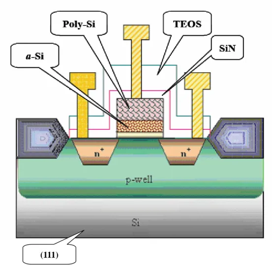
The local strained structure with the stack of amorphous Si and SiN-capping layer has been fabricated. The schematic cross section is illustrated in Figure 2-1. After BF2
implantation for p-well region, CVD SiO2 for oxidation enhanced diffusion (OED) in
well drive-in process was executed. Pad oxide and Si3N4 were deposited and active
region alignment was followed. After Si3N4 etching, BF2 was implanted for the sake
of channel stop. Then, field oxidation was carried out in high temperature ambience for LOCOS isolation. Two times of sacrificial oxide growth followed Si3N4 removal
process to eliminate Kooi effect. To adjust threshold voltage, BF2 was
implanted(50KeV, 5E12). After RCA cleaning process, 2nm gate oxide was grown in a vertical furnace (800oC, O2 ambience).The stacked gate, a-Si (amorphous silicon)
(550oC, 20-70nm) and in-situ doped n+ poly-Si (550oC) were deposited in the same ambience followed by gate oxidation. The total thickness of poly-gate for all sample was 200nm.Then, poly-Si and a-Si were etched followed gate alignment process. To prevent the leakage surrounding the gate edge, a poly reoxidation process was added here. After sidewall polymer removal, wafers underwent n+-source/drain implantation (As, 20keV, 5E15) followed alignment process. P+-substrate alignment and
implantation (BF2, 50keV, 2.5E15) was executed and then rapid thermal annealing
was carried out in nitrogen ambience at 1050oC for 10 seconds. Thermal CVD SiN layer (at 780oC) with different thickness, 100-300nm, was directly deposited on the transistor and followed by TEOS deposition (700oC, 350-450nm). After contact alignment, contact etch was acted by etching TEOS and SiN. At first we used the dry etching process to remove the upper TEOS and dipped in BOE solution in order to confirm that the TEOS was completely removed. After removing TEOS, we used another recipe to etch the lower SiN layer. In order to protect the Si surface from plasma etching damage, SiN layer was etched by two steps. We calculated the SiN etching rate and left a thin SiN layer about 20nm after etching. Then, we used H3PO4
solution to etch the residual SiN layer. It is necessary to have an over-etching step in this wet etching process to make sure that SiN layer was completely removed. (Ti/ TiN/ Al/ TiN) four-level metallization were then carried out in PVD system and final alignment was followed. After metal etching process, annealing in a H2/ N2 ambience
at 400oC for 30 minutes was performed in order to mend dangling bonds and reduce interface state density in oxide/ Si interface.
Fig. 2-1 Schematic cross section of the local strained channel nMOSFET on (111) substrate
Chapter 3
Results and Discussion
3-1 Single-poly-Si gate structure with different thickness of SiN-capping layer
At first, we discuss the characteristics of the structure with single-poly-Si gate and
different thickness of SiN layer. The relation of Id-Vg characteristics with different
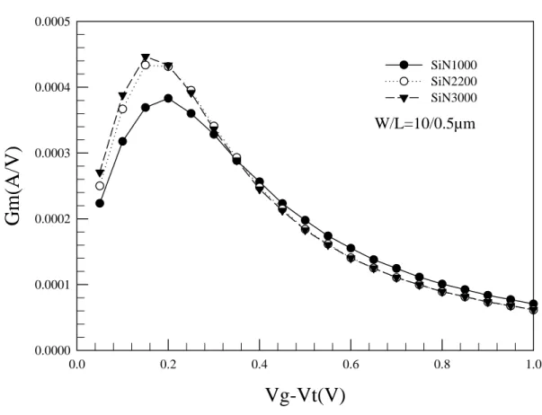
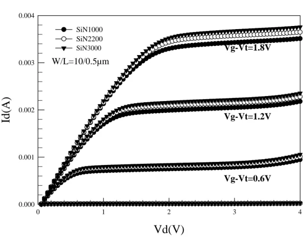
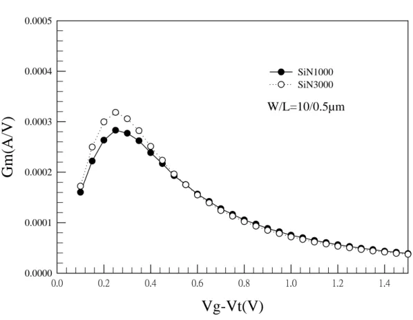
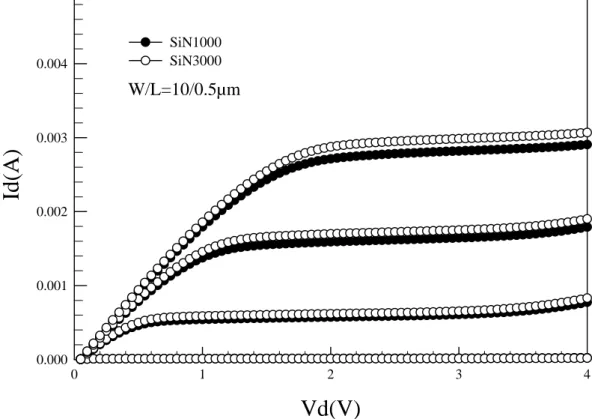
SiN layer thickness is shown in Figure 3-1. The dependence of linear transconductance and the thickness of SiN layer is shown in Figure 3-2. The output characteristics Id-Vd of the devices with different SiN layer thickness is shown in
Figure 3-3. The improvement of drain current and transconductance is proportional to the thickness of SiN layers. The mechanism which results in these results might be as follows: These SiN capping layers upon the poly-Si gates with highly tensile stress cause the poly-Si gates under them to be with compressive strain, and then the tensile strain is caused in the channel regions by these compressive poly-Si gates upon channel regions. The results might also be caused by another mechanism: The SiN capping layers with highly tensile stress are directly deposited on the source/drain regions in the two terminals of channels. These SiN layers cause the source/drain regions under them compressive and the channel regions are implicated to become tensile. The strain causes the sixfold degenerate valleys of the silicon conduction band
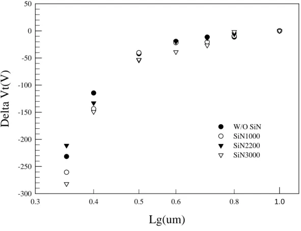
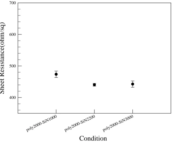
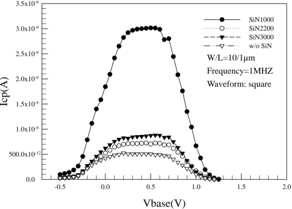
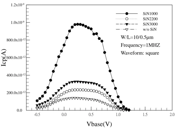
minimum to split into two groups: two lower valleys with longitudinal effective mass axis perpendicular to the interface, and four raised valleys with the longitudinal mass axis parallel to the interface. This splitting suppresses the intervalley transitions of electrons from lower valleys to upper valleys, thus reduces the intervalley scattering. In addition, in the lower valleys, electrons show the smaller effective mass in transport parallel to the interface. The combination of the reduced intervalley phonon scattering and the light effective mass gives rise to higher electron mobility. Figure 3-4 shows the Vt-roll-off characteristics depending on different thickness of SiN layer. Figure 3-5 shows the threshold voltages for the devices with different thickness of SiN layers. The Vt-roll-off phenomenon is getting serious when the SiN layer is getting thicker. This implies that short channel effect is more serious while the SiN layer is getting thicker. The threshold voltages of the devices with SiN layer are larger than those without SiN layers, but degrade with the increasing thickness of SiN layers. This maybe is due to a long processing time for deposition of thicker SiN film. Figure 3-6 shows the sheet resistance of gate for different thickness of SiN layer. There is not apparent trend in sheet resistance of gate for different thickness of SiN layer. In other word, sheet resistance of gate is not affected by the SiN capping layer. Figure 3-7 shows the charge pumping current of the device with 1-µm gate length for different thickness of SiN layer, and Figure 3-8 shows that of the device with 0.5-µm gate
length. The charge pumping current illustrates the quality of oxide/Si interface after the strain is induced in the channel region. The device without SiN capping layer has the smallest charge pumping current. Capping SiN layer may cause more interface state at the oxide/Si interface, but the charge pumping current decreases as the SiN layer thickness increases. This means that although SiN capping layer may cause some damage at the oxide/Si interface, the SiN layer capping process may provide some hydrogen atoms separated from the NH3 gas to passivate the interface state with
the process proceeding. The thicker the SiN layer capping, the longer time the process need and the more interface states was passivated. Figure 3-9 shows the transconductance characteristics of the devices with different thickness of SiN capping layers at 125oC. Figure 3-10 shows the Id-Vd characteristics of devices at
125oC. Compare to the device with thinner SiN layer (1000Å), the device with 3000Å SiN layer has higher transconductance and the improvement is 11.1% at room temperature (Figure 3-2) and 11.5% at 125oC. Besides, in the Id-Vd characteristics, the
device with 3000Å SiN layer shows 6.9% improvement compared with one with 1000Å SiN layer at room temperature (Figure 3-3). This improvement of Id-Vd characteristics at 125oC is 6.0%. As Figure3-11 shows, as the temperature rises to 125oC, the transconductance of the device with 1000Å SiN layer is degraded by 27.5% and that of the device with 3000Å SiN layer is degraded by 26.3%. Besides,
Figure 3-12 shows that as the temperature rises to 125oC, the Idsat of the device with
1000Å SiN layer is degraded by 17.2% and that of the device with 3000Å SiN layer is degraded by 18%. From those result we observed that the thickness of SiN layer does not apparently influences the temperature dependence of the devices.
Poly2000-SiN split
Vg-Vt(V)
0.0 0.5 1.0 1.5 2.0 2.5Id(A)
0.00000 0.00005 0.00010 0.00015 0.00020 0.00025 0.00030 SiN1000 SiN2200 SiN3000Fig. 3-1 Id-Vg characteristics for different thickness of SiN-capping layer W/L=10/0.5µm
poly2000-SiN split
Vg-Vt(V)
0.0 0.2 0.4 0.6 0.8 1.0Gm(A/V)
0.0000 0.0001 0.0002 0.0003 0.0004 0.0005 SiN1000 SiN2200 SiN3000Fig. 3-2 Gm-Vg characteristics for different thickness of SiN-capping layer W/L=10/0.5µm
Poly2000-SiN split
Vd(V)
0 1 2 3 4Id(A)
0.000 0.001 0.002 0.003 0.004 SiN1000 SiN2200 SiN3000Fig. 3-3 Id-Vd characteristics for different thickness of SiN-capping layer
Vg-Vt=1.2V Vg-Vt=1.8V
Vg-Vt=0.6V
poly-2000 SiN split
Lg(um)
0.3 0.4 0.5 0.6 0.8 1.0Del
ta Vt(V)
-300 -250 -200 -150 -100 -50 0 50 W/O SiN SiN1000 SiN2200 SiN3000poly2000-SiN split
Condition
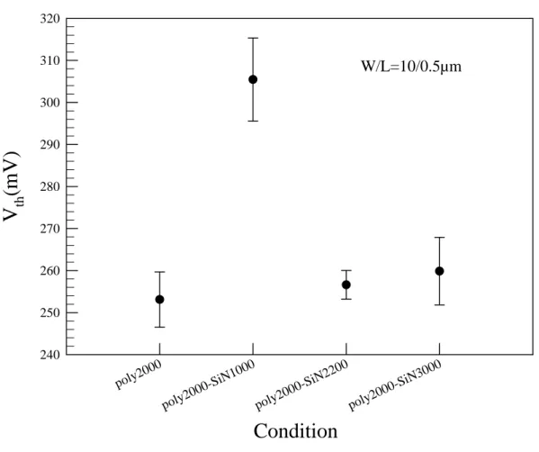
poly20 00 poly20 00-SiN 1000 poly20 00-SiN 2200 poly20 00-SiN 3000V
th(mV)
240 250 260 270 280 290 300 310 320Fig. 3-5 Threshold voltage for different thickness of SiN capping layer
poly2000-SiNsplit
Condition
poly20 00-SiN 1000 poly20 00-SiN 2200 poly20 00-SiN 3000Sheet Resistance(ohm/sq)
400 500 600 700Poly2000-SiN split-1um
Vbase(V)
-0.5 0.0 0.5 1.0 1.5 2.0Icp(A)
0.0 500.0x10⁻¹² 1.0x10⁻⁹ 1.5x10⁻⁹ 2.0x10⁻⁹ 2.5x10⁻⁹ 3.0x10⁻⁹ 3.5x10⁻⁹ SiN1000 SiN2200 SiN3000 w/o SiNFig. 3-7 Charge pumping current for different thickness of SiN layer (Lg=1um)
W/L=10/1µm Frequency=1MHZ Waveform: square
Poly2000-SiN split-0.5um
Vbase(V)
-0.5 0.0 0.5 1.0 1.5 2.0Icp(A)
0.0 200.0x10⁻¹² 400.0x10⁻¹² 600.0x10⁻¹² 800.0x10⁻¹² 1.0x10⁻⁹ 1.2x10⁻⁹ SiN1000 SiN2200 SiN3000 w/o SiNFig. 3-8 Charge pumping current for different thickness of SiN layer (Lg=0.5um)
W/L=10/0.5µm Frequency=1MHZ Waveform: square
poly2000-SiN split 125
oC
Vg-Vt(V)
0.0 0.2 0.4 0.6 0.8 1.0 1.2 1.4Gm(A/V)
0.0000 0.0001 0.0002 0.0003 0.0004 0.0005 SiN1000 SiN3000Fig. 3-9 Gm-Vg characteristics for different thickness of SiN-capping layer at
125oC
Poly2000-SiN split 125
oC
Vd(V)
0 1 2 3 4Id(A)
0.000 0.001 0.002 0.003 0.004 0.005 SiN1000 SiN3000Fig. 3-10 Id-Vd characteristics for different thickness of SiN-capping layer at
125oC
Gm_Vg-Vt at different temperature
Vg-Vt(V)
0.0 0.2 0.4 0.6 0.8 1.0 1.2 1.4Gmlin(A/V)
0.0000 0.0001 0.0002 0.0003 0.0004 0.0005 125oC Gm SiN1000 room temp Gm SiN1000 125oC Gm SiN3000 room temp Gm SN3000Fig. 3-11 Gm-Vg characteristics for different thickness of SiN layer at different
temperature
Id-Vd at different temperature
Vd(V)
0 1 2 3 4Id(A)
0.000 0.001 0.002 0.003 0.004 125oC SiN1000 room temp SiN1000 125oC SiN3000 room temp SiN3000Fig. 3-12 Id-Vd characteristics for different thickness of SiN layer at different
temperature
3-2 Stack of a-Si and Poly-Si gate with fixed thickness of SiN-capping layer
In this section, we would talk about the strain effect of the stack of amorphous silicon and poly silicon in the gate structure. Each sample is capped by a 1500Å SiN layer. The relation of Id-Vg characteristics and the thickness of a-Si layer is shown in
Figure 3-13. The dependence of linear transconductance and the thickness of a-Si layer is shown in Figure 3-14. The drain current and transconductance are improved as the thickness of a-Si layer increases. This result implies that there is strain dependence of mobility enhancement by stack of a-Si gate structure. We can observed that the difference of strain effect between the devices with 500Å and 700Å a-Si layers is not very apparent compared with which between the devices with 200Å and 500Å a-Si layers. It might mean that the strain effect is getting saturate when the thickness of a-Si layer is up to 500Å. The mechanism of the stress elevation could be as follows: before the dopant activation process, the n+-poly gate is in amorphous phase due to due to the stack of a-Si and high dose implantation of arsenic. The re-crystallization of amorphous region during rapid thermal annealing leads to n+-poly gate expansion and residual compressive stress. Therefore, the compressive stress in the n+-poly gate provides tensile strain to the channel region. The output characteristics Id-Vd of the devices with different a-Si layer thickness is shown in
which with 200Å a-Si layer is 10.2%, and the on current improvement of that is 6.7%. Figure 3-16 shows the Vt-roll-off characteristics depending on different thickness of a-Si layer. Figure 3-17 shows the threshold voltages for the devices with different thickness of a-Si layers. The threshold voltage of the device with thick a-Si layer is apparently larger than that of the device with thin a-Si layer. This result might be due to the wider poly depletion region in the stack gate structure with thicker a-Si layer. As the total thicknesses of all the stack gate structures are the same, the in-situ doping dose is getting lower when the in situ-doped poly-Si layer is getting thinner. After annealing, the doping concentration of the stack gate with thinner poly-Si layer and thicker a-Si layer becomes lower than the others. Lower doping concentration in the gate causes wider poly depletion region, and decreased the gate capacitance. As a result, the threshold voltage is increased when the stack gate structure is with thicker a-Si layer. Figure 3-18 shows the sheet resistance of gate for different thickness of a-Si layer. The sheet resistance of gate is also apparently higher in a stack gate structure with thicker a-Si layer. It tells the lower doping concentration was found in the stack gate structure with thicker a-Si layer, and this result can be an evidence of the of Vth variation mentioned above. Figure 3-19 shows the charge pumping current of the device with 1-µm gate length for different thickness of a-Si layer, and Figure 3-20 shows that of the device with 0.5-µm gate length. There is an interesting
phenomenon that the charge pumping current of the device with 500Å a-Si layer is highest in these samples. It tells that the device with 500Å a-Si layer has more oxide / Si interface state than that with 200Å and 700Å a-Si layer. Figure 3-21 shows the transconductance characteristics of the devices with different thickness of a-Si capping layers at 125oC. Figure 3-22 shows the Id-Vd characteristics of devices measured at 125oC. Compare to the device with 200 Å a-Si layer, the device with 700Å a-Si layer has higher transconductance and the improvement is 10.2% at room temperature (Figure 3-14) and 16.3% at 125oC. Besides, in the Id-Vd characteristics, the device with 700Å a-Si layer shows 6.6% improvement compared with that with 200Å a-Si layer at room temperature (Figure 3-15). This improvement of Id-Vd characteristics at 125oC is 33%. As Figure3-23 shows, as the temperature rises to 125oC, the transconductance of the device with 200Å a-Si layer is degraded by 33.1% and that of the device with 700Å a-Si layer is degraded by 29.5%. Besides, Figure 3-24 shows that as the temperature rises to 125oC, the Idsat of the device with 200Å
a-Si layer is degraded by 36.6% and that of the device with 700Å a-Si layer is degraded by 21%. It is observed that the stack structure is influenced by temperature more easily compared by SiN capping layer structure. Although the improvement between different thicknesses of a-Si layer is increased at elevated temperature, the degradation of the performance of these devices with stack structure is serious,
a-Si split-SiN1500
Vg-Vt(V)
0.0 0.5 1.0 1.5 2.0 2.5Id(A)*Tox(10
-10
m)
0.000 0.001 0.002 0.003 0.004 0.005 0.006 0.007 a200 a500 a700Fig. 3-13 Id-Vg characteristics for different thickness of amorphous Si layer W/L=10/0.5µm
a-Si split-SiN1500
Vg-Vt(V)
0.0 0.2 0.4 0.6 0.8 1.0 1.2 1.4Gm(A/V) * Tox(10
-10m)
0.000 0.002 0.004 0.006 0.008 0.010 a-200 a-500 a-700Fig.3-14 Gm-Vg characteristics for different thickness of amorphous Si layer W/L=10/0.5µm
a-Si split-SiN1500
Vd(V)
0 1 2 3 4Id(A)*Tox(10
-10
m)
0.00 0.02 0.04 0.06 0.08 0.10 a200 a500 a700Fig. 3-15 Id-Vd characteristics for different thickness of amorphous Si layer
Vg-Vt=1.8V
Vg-Vt=1.2V
Vg-Vt=0.6V
a-Si split-SiN1500
Lg(um)
0.3 0.4 0.5 0.6 0.8 1Del
ta Vt(V)
-300 -250 -200 -150 -100 -50 0 50 100 a-200 a-500 a-700a-Si split-SiN1500
Condition
a200-SiN1500 a500-SiN1500 a700-SiN1500
V
th
(mV)
240 250 260 270 280 290 300 310 320Fig. 3-17 Threshold voltage for different thickness of amorphous Si layer
a-Si split-SiN1500
Condition
a200-SiN1500 a500-SiN1500 a700-SiN1500
She
et
Re
sist
ance
(ohm/
sq)
400 500 600 700 800a-Si split-SiN 1500-1um
Vbase(V)
-1.0 -0.5 0.0 0.5 1.0 1.5 2.0I cp
(A)
0.0 200.0x10⁻¹² 400.0x10⁻¹² 600.0x10⁻¹² 800.0x10⁻¹² 1.0x10⁻⁹ 1.2x10⁻⁹ 1.4x10⁻⁹ 1.6x10⁻⁹ a-200 a-500 a-700Fig. 3-19 Charge pumping current for different thickness of amorphous Si layer (Lg=1um)
W/L=10/1µm Frequency=1MHZ Waveform: square
a-Si split-SiN 1500-0.5um
Vbase(V)
-1.0 -0.5 0.0 0.5 1.0 1.5 2.0I cp
(A)
0 100x10-12 200x10-12 300x10-12 400x10-12 500x10-12 600x10-12 a-200 a-500 a-700Fig. 3-20 Charge pumping current for different thickness of amorphous Si layer (Lg=0.5um)
W/L=10/0.5µm Frequency=1MHZ Waveform: square
a-Si split-SiN1500 125oC
Vg-Vt(V)
0.0 0.2 0.4 0.6 0.8 1.0 1.2 1.4Gmlin(A/V) * Tox(10
-10
m)
0.000 0.002 0.004 0.006 0.008 0.010 a-200 a-700Fig. 3-21 Gm-Vg characteristics for different thickness of amorphous Si layer at
125oC
a-Si split-SiN1500 125
oC
Vd(V)
0 1 2 3 4Id(A)*Tox(10
-10
m)
0.00 0.02 0.04 0.06 0.08 0.10 a200 a700Fig. 3-22 Id-Vd characteristics for different thickness of amorphous Si layer at
125oC
Gm_Vg-Vt at different temperature
Vg-Vt(V)
0.0 0.2 0.4 0.6 0.8 1.0 1.2 1.4Gm
(A/V)*Tox(10
-10
m)
0.000 0.002 0.004 0.006 0.008 0.010 125oC a-200 room temp a-200 125oC a-700 room temp a-700Fig. 3-23 Gm-Vg characteristics for different thickness of a-Si layer at different
temperature
Id-Vd at different temperature
Vd(V)
0 1 2 3 4Id(A)*Tox(10
-10
m)
0.00 0.02 0.04 0.06 0.08 0.10 125oC a-200 room temp a-200 125oC a-700 room temp a-700Fig. 3-24 Id-Vd characteristics for different thickness of a-Si layer at different
temperature
3-3 Stack of 500Å a-Si gate structure with different thickness of SiN layer
In this section, we integrate SiN capping layer and stack of a-Si gate structures. Each of the samples is with stack of 500Å a-Si layer and different SiN layer thickness in this stage. The relation of Id-Vg characteristics with different SiN layer thickness is
shown in Figure 3-25. The dependence of linear transconductance on the thickness of SiN layer is shown in Figure 3-26. The output characteristics Id-Vd of the devices with
different SiN layer thickness is shown in Figure 3-27. The improvement of drain current and transconductance is proportional to the thickness of SiN layers, but the trend is not very apparent compared with the result of devices with only SiN capping layers discussed in section 3-1. The a-Si layer as a cover might release the strain effect from the SiN capping layer upon it. Figure 3-28 shows the Vt-roll-off characteristics depending on different thickness of SiN layer. Figure 3-29 shows the threshold voltages for the devices with different thickness of SiN layers. The Vt-roll-off phenomenon is getting serious when the SiN layer is getting thicker. This implies that short channel effect is more serious while the SiN layer is getting thicker. The threshold voltages of the devices degrade with the increasing thickness of SiN layers. This maybe is due to a long processing time for deposition of thicker SiN film. This result is similar to devices with only SiN capping layers discussed in section 3-1. Figure 3-30 shows the sheet resistance of gate for different thickness of SiN layer.
There is not apparent trend in sheet resistance of gate for different thickness of SiN layer. In other word, sheet resistance of gate is not affected by the SiN capping layer. Figure 3-31 shows the charge pumping current of the device with 1-µm gate length for different thickness of SiN layer, and Figure 3-32 shows that of the device with 0.5-µm gate length. As we explained in section 3-1, the charge pumping current illustrates the quality of oxide/Si interface with the strain induced in the channel region. The device without SiN capping layer has the smallest charge pumping current. Capping SiN layer may cause more interface states at the oxide/Si interface, but the charge pumping current decreases as the SiN layer thickness increases. This means that although SiN capping layer may cause some damage at the oxide/Si interface, the SiN layer capping process may provide some hydrogen atoms separated from the NH3
gas to passivate the interface state with the process proceeding. The thicker the SiN layer capping, the longer time the process need and the more interface states was passivated. Figure 3-33 shows the transconductance characteristics of the devices with different thickness of SiN capping layers at 125oC. Figure 3-34 shows the Id-Vd
characteristics of devices at 125oC. Compared to the device with thinner SiN layer (1000Å), the device with 3000Å SiN layer has higher transconductance and the improvement is 6.1% at room temperature (Figure 3-26) and 8.6% at 125oC. Besides, in the Id-Vd characteristics, the device with 3000Å SiN layer shows 4.8%
improvement compared with one with 1000Å SiN layer at room temperature (Figure 3-27). This improvement of Id-Vd characteristics at 125oC is 5.7%. As Figure3-35 shows, as the temperature rises to 125oC, the transconductance of the device with 1000Å SiN layer is degraded by 26.2% and that of the device with 3000Å SiN layer is degraded by 25.6%. Besides, Figure 3-36 shows that as the temperature rises to 125oC, the Idsat of the device with 1000Å SiN layer is degraded by 16% and that of the device
with 3000Å SiN layer is degraded by 15.2%. As we observed in section 3-1, the thickness of SiN layer does not apparently influences the temperature dependence of the devices. From all the results shown in this section, we can conclude that except for the apparent degradation of performance improvement shown in Figure 3-25 ~Figure 3-27, almost the trends of those devices with 500Å a-Si stack gate and different SiN layer thicknesses are similar to those with only different SiN layer thicknesses.
a500-SiN split
Vg-Vt(V)
0.0 0.5 1.0 1.5 2.0 2.5Id(A)
0 50x10-6 100x10-6 150x10-6 200x10-6 250x10-6 300x10-6 SiN1000 SiN1500 SiN2200 SiN3000Fig. 3-25 Id-Vg characteristics for different thickness of SiN capping layer W/L=10/0.5µm
a500-SiN split
Vg-Vt(V)
0.0 0.2 0.4 0.6 0.8 1.0 1.2 1.4Gm(A/
V
)
0.0000 0.0001 0.0002 0.0003 0.0004 0.0005 SiN1000 SiN1500 SiN2200 SiN3000Fig. 3-26 Gm-Vg characteristics for different thickness of SiN-capping layer W/L=10/0.5µm
a500 with SiN
Vd(V)
0 1 2 3 4Id
(A
)
0.000 0.001 0.002 0.003 0.004 SiN1000 SiN2200 SiN3000Fig. 3-27 Id-Vd characteristics for different thickness of SiN-capping layer W/L=10/0.5µm
a-500_SiN split
Lg(um)
0.3 0.4 0.5 0.6 0.8 1.0Del
ta Vt(V)
-400 -300 -200 -100 0 w/o SiN SiN1000 SiN1500 SiN2200 SiN3000a500-SiN split
Condition
a500-S iN1000 a500-S iN1500 a500-S iN2200 a500-S iN3000V
th(m
V)
280 285 290 295 300 305 310 315 320Fig. 3-29 Threshold voltage for different thickness of SiN capping layer
a500-SiN split
Condition
a500-S iN1000 a500-S iN1500 a500-S iN2200 a500-S iN3000Shee
t Re
sist
anc
e(ohm/
sq)
400 500 600 700 800a-500-SiN split-1um
Vbase(V)
-0.5 0.0 0.5 1.0 1.5 2.0Icp(A)
0.0 500.0x10⁻¹² 1.0x10⁻⁹ 1.5x10⁻⁹ 2.0x10⁻⁹ SiN1000 SiN1500 SiN2200 SiN3000 W/O SiNFig. 3-31 Charge pumping current for different thickness of SiN layer (Lg=1um)
W/L=10/1µm Frequency=1MHZ Waveform: square
a-500-SiN split-0.5um
Vbase(V)
-0.5 0.0 0.5 1.0 1.5 2.0Icp(A)
0 100x10-12 200x10-12 300x10-12 400x10-12 500x10-12 600x10-12 SiN1000 SiN1500 SiN2200 SiN3000 W/O SiNFig. 3-32 Charge pumping current for different thickness of SiN layer (Lg=0.5um)
W/L=10/0.5µm Frequency=1MHZ Waveform: square
a500-SiN split 125
oC
Vg-Vt(V)
0.0 0.2 0.4 0.6 0.8 1.0 1.2 1.4Gm(A/V)
0.0000 0.0001 0.0002 0.0003 0.0004 0.0005 SiN1000 SiN3000Fig. 3-33 Gm-Vg characteristics for different thickness of SiN-capping layer at
125oC
a500-SiN split at 125
oC
Vd(V)
0 1 2 3 4Id(A)
0.000 0.001 0.002 0.003 0.004 SiN1000 SiN3000Fig. 3-34 Id-Vd characteristics for different thickness of SiN-capping layer at
125oC
Gm_Vg-Vt at different temperature
Vg-Vt(V)
0.0 0.2 0.4 0.6 0.8 1.0 1.2 1.4Gm(A/V)
0.0000 0.0001 0.0002 0.0003 0.0004 0.0005 125oC SiN1000 room temp. SiN1000 125oC SiN3000 room temp. SiN3000Fig. 3-35 Gm-Vg characteristics for different thickness of SiN layer at different
temperature
Id-Vd at different temperature
Vd(V)
0 1 2 3 4Id(A)
0.000 0.001 0.002 0.003 0.004 125oC SiN1000 room temp. SiN1000 125oC SiN3000 Vd vs roomSiN3000Fig. 3-36 Id-Vd characteristics for different thickness of SiN layer at different
temperature
3-4 Comparison of strain effect on different substrate
Finally, we would compare the strain effect on (100) and (111) substrate. Table 3-1
shows the comparison of some characteristics improvement of strained devices on (100) and (111) substrates. The strain effect by SiN capping layer or a-Si layer on (111) substrate is both slightly smaller than that on (100) substrate. The most different trend is observed in the structure with both a-Si layer and SiN capping layer. The strain effect is added by the structure with both a-Si layer and SiN capping layer on (100) substrate showing the largest improvement. However, the structure with both a-Si layer and SiN capping layer on (111) substrate shows smallest improvement.
Poly2000-SiN split
(100)
(111)Gm improvement (%) 12.7% 10.6%
Ion improvement (%) 17.4% 9.4%
a-Si split-SiN fixed
(100)
(111)Gm improvement (%) 3.6% 8.3%
Ion improvement (%) 9.4% 6.8%
a-500-SiN split
(100)
(111)Gm improvement (%) 13.3% 6.8%
Ion improvement (%) 19.3% 2.6%
Chapter 4
Summary and Conclusion
In summary, we investigate that the local strain channel technique using deposition of SiN layer and stack of a-Si gate structure used in the (111) substrate. The device performance is improved as the SiN capping layer or a-Si layer is getting thicker. However, the device with both a-Si layer of gate structure and SiN capping layer shows only slightly strain effect by different thickness of SiN capping layer. The a-Si layer as a cover might release the strain effect from the SiN capping layer upon it. Stack of a-Si gate structure also influences the threshold voltage and sheet resistance of gate because of its poly depletion width. SiN capping layer causes more interface states in oxide / Si interface and serious short channel effect. Finally we compare the strain effect on (100) and (111) substrate. The trends are almost the same except the structure with both a-Si layer and SiN capping layer. Although there are still some challenges, the local strain channel technique used in (111) substrate will be useful to CMOS technology in the future.
Reference
[1] R. Ohba and T. Mizuno, “Non-stationary electron/hole transport in sub-0.1μm MOS devices---Correlation with mobility and low-power CMOS application,” IEEE Trans. Electron Devices, vol. 48, pp. 338-343, Feb. 2001.
[2] F. Gámiz, J. B. Roldán, J. A. López-Villanueva, and P. Cartujo, “Coulomb scattering in strained-silicon inversion layers on Si1-xGex substrate,” Appl. Phys. Lett. 69 No.6, pp. 797-799 5 Aug 1996.
[3] Shin-ichi Takagi, Judy L. Hoyt, Jeffrey J. Weiser, and James F. Gibbons,
“Comparative study of phonon-limited mobility of two-dimensional electrons in strained and unstrained Si metal-oxide-semiconductor field-effect transistors,” Appl. Phys. Lett. 80 No.3, pp. 1567-1577 1 Aug 1996.
[4] Sarah H. Olsen, Anthony G. O’Neill, Sanatan Chattopadhyay, Luke S. Driscoll, K. S. K. Kwa, D. J. Norris, A. G. Cullis, and Douglas J. Paul, Member, IEEE, “Study of Single- and Dual-Channel Desighs for High-PERformance
Strained-Si-SiGe n-MOSFETs,” IEEE Trans. Electron Devices, vol. 51, pp. 1245-1253, July 2004.
[5] Haizhou Yin, K. D. Hobart, Rebecca L. Peterson, F. J. Kub, S. R. Shieh, T. S. Duffy, and J. C. Sturm, “Fully-depleted Strained-Si on Insulator NMOSFETs without Relaxed SiGE Buffers,” IEDM Tech. Dig., pp. 53-56 2003.
[6] Issac Lauer, T. A. Langdo, Z. –Y. Cheng, J. G. Fiorenza, G. Breithwaite, M. T. Currie, C. W. Leitz, A. Lochtefeld, H. Badawi. M. T. Bulsara, M. Somerville, and D. A. Antoniadis, Fellow, IEEE, “Fully Depleted n-MOSFETs on Supercritical Thickness Strained SOI,” IEEE Electron Device Lett., vol. 25, pp. 83-85, Feb. 2004.
[7] K. Rim, K. Chan, L. Shi, D. Boyd, J. Ott, N. Klymko, F. Cardone, L. Tai, S. Koester, M. Cobb, D. Canaperi, B. To, E. Duch, I. Babich, R. Carruthers, P. Saunders, G. Walker, Y. Zhang, M. Steen, and M. Ieong, “Fabrication and
Mobility Characteristics of Untra-thin Strained Si Directly on Insulator (SSDOI) MOSFETs,” IEDM Tech. Dig., 2003.
[8] J. R. Hwang, J. H. Ho,S.M. Ting, T.P. Chen, Y. Y. Hsieh, C. C. Huang, Y. Y. Chiang, H. K. Lee, Ariel Liu, T.M. Shen, G. Braithwaite, M. Currie, N, Gerrish, R. Hammond, A. Lochtefeld, F. Singaporewala, M. Bulsara, Q. Xiang, M. R. Lin, W. T. Shiau, Y. T. Loh, J. K. Chen, S. C. Chien, and Frank Wen, “Performance of 70nm Strained-Silicon CMOS Devices,” VLSI Symp. Tech. Dig., pp. 103-104, 2003.
[9] T. Ghani, M. Armstrong, C. Auth, M. Bost, P. Charvat, G. Glass, T. Hoffmann, K. Johnson, C. Kenyon, J. Klaus, B. McIntyre, K. Mistry, A. Murthy, J. Sandford, M. Silberstein, S. Sivakumar, P. Smith, K. Zawadzki, S. Thompson and M. Bohr, “A
90nm High Volume Manufacturing Logic Technology Featuring Novel 45nm Gate length Strained Silicon CMOS Transistors,” IEDM Tech. Dig., 2003. [10] K. Mistry. M. Armstrong, C. Auth, S. Cea, T. Coan, T. Ghani, T. Hoffmann, A.
Murthy, J. Standford, R. Shaheed, K. Zawadzki, K. Zhang, S. Thompson and M. Bohr, “Delaying Forever: Uniaxial Strained Silicon Transistors in 90nm CMOS technology,” VLSI Symp. Tech. Dig., pp. 50-51, 2004.
[11] Scott E. Thompson, Member, IEEE, Mark Armstrong, Chis Auth, Steve Cea, Robert Chau,Glenn Glass, Thomas Hoffman. Jason Klaus, Zhiyoug Ma, Brain Mcintyre, Anand Murthy, Borna Obradovic, Lucian Shifren, Sam Sivakumar, Sunit Tyagi, Tahir Ghani, Kaizad Mistry, Member, IEEE, Mark BohR,Fellow, IEEE, And Youssef El-Mansy, Fellow, IEEE, “A Logic Nanotechnology
Featuring Strained-Silicon,” IEEE Electron Device Lett., vol. 15, pp. 83-85, Apr. 2004.
[12] Jung-Suk Goo, Member, IEEE, Qi Xiang , Yayoi TAkamura, Student Member, IEEE, Haihong Wang, James Pan, Farzad Arasnia, Eric N. Paton, Paul Besser,
Maxim V. Sidorov, Ercan Adem, Anthony Lochtefeld, Member, IEEE, Glyn Braithwaite, Matthew T. Currie, Member, IEEE, Richard Hammond, Mayank T. Bulsara, Member, IEEE, and Ming-Ren Lin, “Scalability of Strained-Si
pp. 83-85, May. 2003.
[13] A. Shimizu, K. Hachimine, N. Ohki, H. Ohta, M. Koguchi, Y. Nonaka, H. Sato, and F. Ootsuka, “Local Mechanical-Stress Control (LMC) : A New Technique for CMOS-Performance Enhancement,” IEDM Tech. Dig., 2001.
[14] S. Pidin, T. Mori, R. Nakamura, T. Saiki, R. Tanabe, S. Satoh, M. Kase, K. Hashimoto, and T. Sugii, “MOSFET Current Drive Optimization Using Silicon Nitride Capping Layer for 65-nm Technology Node,” VLSI Symp. Tech. Dig., pp. 54-55, 2004.
[15] Shinya Ito, Hiroaki Namba, Kensuke Yamaguchi, Tsuyoshi Hirata, Koichi Ando, Shin Koyama, Shunichiro Kuroi, Nobuyaki Ikezawa, Tatsuya Suzuki, Takechiro Saitoh, and Tadahiko Horiuchi, “Mechanical Stress Effect of Etch-Stop Nitride and its Impact on Deep Submicron Transistor Design,” IEDM Tech. Dig., 2000. [16] S. Maikap, C. –Y. Yu, S. –R. Jan, M. H. Lee, and C. W. Liu, Senior Member,
IEEE, “Mechanically Strained Strained-Si NMOSFETs,” IEEE Electron Device
Lett., vol. 25, pp. 40-42, Jan. 2004.
[17] Y. G. Wang, D. B. Scott, J. Wu, J. L. Waller, J. Hu, K. Liu, and V. Ukraintsev, “Effect of Uniaxial Mechanical Stress on Drive Current of 0.13μm MOSFETs,” IEEE Trans. Electron Devices, vol. 50, pp. 529-531, Feb 2003.
Chung, Hung-Wai Chen, Chang-Yun Chang, Cheng-Chuan Huang, Kuang-Hsin Chen, Di-Hong LeE, Hsun-ChiH Tsao, Cheng-Kuo Wen, Shui-Ming Cheng, Yi-Ming Sheu, Ke-Wei Su, Chi-Chun Chen, and Chenming Hu, “A 65nm Node Strained SOI Technology with Slim Spacer,” IEDM Tech. Dig., 2003.
[19] C. Gallon, G. Reimbold, Member, IEEE, Gérard Ghibaudo, Senior Member, IEEE, R. A. Bianchi, R. Gwoziecki, S. Orain, E. Robilliart, C. Raynaud, and H. Dansas, “Electrical Analysis of Mechanical Stress Induced by STI in Short MOSFETs Using Externally Applied Stress,” IEEE Trans. Electron Devices, vol. 51, pp. 1254-1261, Aug. 2004.
[20] T. Sanuki, A. Oishi, Y. Morimasa, S. Aota, T. Kinoshita, R. Hasumi, Y. Takegawa, K.Isobe, H. Yoshimura, M. Iwai, K. Sunouchi and T. Noguchi, “Scalability of Strained Silicon CMOSFET and High Drive Current Enhancement in the 40nm Gate Length Technology,” IEDM Tech. Dig., pp. 65-68, 2003.
[21] F. Ootsuka, S. Wakahara, K. Ichinose, A. Honzawa, S. Wada, H. Sato, T. Ando, H. Ohta, K. Watanabe, and T. Onai, “A Highly Dense, High-Performance 130nm node CMOS Technology for Large Scale System-on-a-Chip Applications” IEDM Tech. Dig., 2000.
[22] Chenming Hu, “DEVICE CHALLENGES AND OPPORTUNITIES” VLSI Symp. Tech. Dig., pp. 4-5, 2004.
[23] C. –H. Ge, C. –C. Lin, C. –H. Ko, C. –C. Huang, B. –W. Chan, B. –C. Perng, C. –C. Sheu, P. –Y. Tsai, L. –G. Yao, C. –L. Wu, T. –L. Lee, C. –J. Chen, C. –T. Wang, S. –C. Lin, Y. –C. Yeo and C. Hu, “Process-Strained Si (PSS) CMOS Technology Featuring 3D Strain Engineering” IEDM Tech. Dig., 2003. [24] Hisayo Sasaki Momose, Senior Member, IEEE, Tatsuya Ohguro, Shin-ichi
Nakamura, Yoshiaki Toyoshima, Member, IEEE, Hidemi Ishiuchi, Member, IEEE, and Hiroshi Iwai, Fellow, IEEE, “Ultrathin Gate Oxide CMOS on (111)
Surface-Oriented Si Substrate,” IEEE Trans. Electron Devices, vol. 49, pp. 1597-1605, Sep. 2002.
[25] Tien Sheng Chao, Senior Member, Yu Hsin Lin, and Wen Luh Yang, “Mobility Enhancement of MOSFETs on p-Silicon (111) with In Situ HF-Vapor Pre-Gate Oxide Cleaning,” IEEE Electron Device Lett., vol. 25, pp. 625-627, Sep. 2004.
![TraditionalMLCalgorithmsmainlytacklethebatchMLCproblem,wheretheinputdataarepresentedinabatch[24,28].Nevertheless,inmanyMLCapplicationssuchase-mailcategorization[22],multi-labelexamplesarriveasastream.Onlineanalysisistherefore dimensionreducermotivatedbyma](data:image/gif;base64,R0lGODlhAQABAIAAAP///wAAACH5BAEAAAAALAAAAAABAAEAAAICRAEAOw==)