國
立
交
通
大
學
電子工程學系 電子研究所碩士班
碩
士
論
文
利用複數導數相消之低功率、高線性
度混波器
Low-Power and High-Linearity Mixer Adopting Derivative
Cancellation by Complex Transconductance Equivalent
Circuit
研 究 生:詹維嘉
指導教授:郭建男 教授
利用複數導數相消之低功率、高線性度混波器
Low-Power and High-Linearity Mixer Adopting Derivative
Cancellation by Complex Transconductance Equivalent
Circuit
研 究 生:詹維嘉 Student:Wei-Chia Zhan
指導教授:郭建男
Advisor:Chien-Nan Kuo
國 立 交 通 大 學
電子工程學系 電子研究所碩士班
碩 士 論 文
A ThesisSubmitted to Department of Electronics Engineering & Institute of Electronics College of Electrical Engineering and Computer Science
National Chiao Tung University In Partial Fulfillment of the Requirements
For the Degree of Master
In
Electronic Engineering July 2005
Hsinchu, Taiwan, Republic of China
利用複數導數相消之低功率、高線性度混波器
學生 : 詹 維 嘉 指導教授 : 郭 建 男 教授
國立交通大學
電子工程學系 電子研究所碩士班
摘要
本篇論文提出一個複數轉導的等效電路,藉此應用於多閘極架構之線性度分 析,相較於之前所提出的分析,此複數轉導能得到更精確之元件參數,以利於電 路設計之用。根據此種分析方法,折疊式混頻器與前端電路分別經由晶片製作來 驗證。 第一顆晶片在於設計與分析應用於無線區域網路之低功率、高線性度之混頻 器。量測結果顯示此一混頻器在只消秏1.8 mW 之功率損秏下,有著 4.7 dB 之轉 換增益,9 dB 之輸入反迴損秏以及 10.3 dBm 之輸入第三階交會點。 在第二顆晶片中,適用於無線區域網路接收端之低功率前端電路被設計與分 析,此電路包含了一個低雜訊放大器,一個相位分離器以及一個直接降頻混頻器。 量測結果顯示此前端電路有9.5 dB 的轉換增益,21.5 dB 之輸入反迴損秏以及-2.6 dBm 之輸入第三階交會點,此外此電路消秏之功率為 10.1mW.Low-Power and High-Linearity Mixer Adopting Derivative
Cancellation by Complex Transconductance Equivalent
Circuit
Student: Wei-Chia Zhan Advisor: Prof. Chien-Nan Kuo
Department of Electronics Engineering & Institute of Electronics
National Chiao-Tung University
ABSTRACT
A compact equivalent circuit using a complex transconductance is proposed for linearity design in the multiple gated transistors configuration. This complex transconductance gives better design parameters as compared to previous published analysis. Following the complex transconductance analysis, a folded mixer and a front-end circuit were verified through two individual.
In the first chip, a low-power and high-linearity mixer is analyzed and designed for wireless local area network. Measured data shows that the designed mixer has conversion gain of 4.7 dB, input return loss of 9 dB, and input third-order intercept point (IIP3) of 10.3 dBm with only 1.8 mW power dissipation.
In the second chip, a low-power front-end circuit, intended for use in the receiver path of the wireless local area network systems, is analyzed and designed. This front-end circuit is composed of a low noise amplifier, a phase splitter, and a direct down-conversion mixer. Measured data shows that the front-end circuit has conversion gain of 9.5 dB, input return loss of 21.5 dB, input third-order intercept point (IIP3) of -2.6 dBm, while consuming only 10.1mW.
ACKNOWLEDGEMENTS
能夠完成此篇論文,首先要感謝我的指導教授郭建男教授這兩年以來給我的 指導與鼓勵,使我在射頻積體電路的領域中有所了解,更學習到許多做學問的態 度與方法,在此向老師獻上最深最深的敬意。 另外要感謝郭治群教授在低功率計畫中給於我很多指導及支持。感謝昶綜、 鈞琳、上逸、健嘉、敬銘、英瑞、志修、宏達、柏之學長在研究及學業上給我很 多的幫助。還有一起奮鬥的仰鵑、坤宏、政偉,以及岱原、子倫、達道、冠華、 杰利、宜岑、燕霖、俊興、宗男、俊凱學弟妹,大家一起做研究、打球、出遊, 就像一個大家庭,使我在兩年的碩士生活中留下許多美好的回憶。還要感謝溫老 師及國家晶片中心在晶片製作和量測上的大力幫忙,使我能夠順利的完成這篇論 文。 最後還要感謝我的父母給我的栽培及鼓勵,以及瀞瑩在精神上給我許多的支 持,使我能順利走完碩士這段路程。其他要感謝的人還有很多,在此一併謝過 詹維嘉 九四年七月CONTENTS
ABSTRACT (CHINESE) ...i
ABSTRACT (ENGLISH)...ii
ACKNOWLEDGEMENTS ... iii
CONTENTS...iv
TABLE CAPTIONS...vii
FIGURE CAPTIONS ... viii
CHAPTER 1 Introduction ...1
1.1 Motivation ... 1
1.2 Thesis Organization ... 2
CHAPTER 2 Basic Concepts in RF Design...3
2.1 Receiver Architecture ... 3
2.1.1 Heterodyne Receiver
...3
2.1.2 Homodyne Receiver
...4
2.2 Wireless Local Area Network ... 5
2.3 Noise Basic ... 7
2.3.1 Noise Source ...8
2.3.2 Noise Model of MOSFET...9
2.3.3 Noise Figure of Cascaded Stage ...11
2.4 Linearity Basic... 11
2.4.1 Fundamental of the Volterra Series...12
2.4.2 Nonlinear Performance Parameters in Terms of Volterra
Kernels ...13
Circuit Design...17
3.1 Low Noise Amplifier Basic ... 17
3.1.1 Low Noise Amplifier Architecture Analysis...17
3.1.2 Optimizations of Low Noise Amplifier Design Flow...20
3.2 Phase Splitter Basic ... 22
3.3 Down-Conversion Mixer Basic ... 25
3.3.1 Conversion Gain ...26
3.3.2 Switching Stage...27
3.3.3 Mixer Noise...28
3.3.4 Port-to-Port Isolation...29
3.3.5 Linearity ...29
CHAPTER 4 5.5 GHz Low-Power and High-
Linearity Mixer ...30
4.1 Low-Power Design Consideration... 30
4.1.1 Low Voltage Topology ...30
4.1.2 Narrowband Source-Coupled Pair ...31
4.2 Analysis of Linearity ... 34
4.2.1 Nonlinear Effects of Common-Source Amplifier...35
4.2.2 Multiple Gated Transistors Method ...42
4.2.3 Complex Transconductance Analysis ...45
4.3 Chip Implementation and Measured Result... 48
4.3.1 Circuit Implementations...48
4.3.2 Experimental Results ...50
4.3.3 Discussions...55
CHAPTER 5 Low-Power Front-End Circuit ...56
5.2 Principle of the Circuit Design ... 57
5.2.1 Low Noise Amplifier ...57
5.2.2 Phase Splitter...59
5.2.3 Direct Down-Conversion Mixer ...61
5.3 Chip Implementation and Measured Result... 62
5.3.1 Circuit Implementations...62
5.3.2 Experimental Results ...63
5.3.3 Discussions...68
CHAPTER 6 Summary and Future Work ...69
6.1 Summary... 69
6.2 Future Work ... 70
REFERENCES...71
TABLE CAPTIONS
Table 2.1 The set of the channelization………...6 Table 2.2 Rate-dependent parameters………7 Table 2.3 Receiver performance requirements………..7 Table 2.4 Different responses at the output of a nonlinear system described by
Volterra kernels………...14 Table 4.1 Summary of simulation and measured results of MGTR mixer…….….54 Table 4.2 Performance comparison of CMOS mixers……….55 Table 5.1 Summary of simulation and measured results of front-end circuit…….68
FIGURE CAPTIONS
Fig. 2.1 Simple heterodyne architecture……….………...3
Fig. 2.2 Rejection of image versus suppression of interferers for (a) large ωIF (b) small ω ……….…….……..4 IF Fig. 2.3 Simple homodyne receiver architecture……….………..5
Fig. 2.4 802.11a channel distribution……….….………..6
Fig. 2.5 Standard noise model of MOSFET………...…….11
Fig. 2.6 Schematic representation of a system characterized by a Volterra series..12
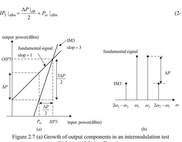
Fig. 2.7 (a) Growth of output components in an intermodulation test (b) Intermodulation distortion………..16
Fig. 3.1 Common-source input stage with inductive source degeneration…….….17
Fig. 3.2 Equivalent noise model of Figure 3.1……….…...18
Fig. 3.3 Differential pair amplifier………..23
Fig. 3.4 Simulated results of Fig. 3.3 (a) phase difference (b) gain error………...24
Fig. 3.5 Phase compensation circuit………....24
Fig. 3.6 Phase splitter with RC compensation………...25
Fig. 3.7 Simplified CMOS Gilbert Cell mixer………...………...…26
Fig. 4.1 Low-voltage topology………...……….31
Fig. 4.2 Source-coupled pair (a) conventional approach (b) narrowband approach...32
Fig. 4.3 (a) Differential input signal (b) Single-ended input signal…….……..….33
Fig. 4.6 Linearized equivalent of the circuit of the Fig. 4.5….………...37
Fig. 4.7 Equivalent circuit for the computation of the second-order kernels in Fig. 4.5...38
Fig. 4.8 Equivalent circuit for the computation of the third-order kernels in Fig. 4.5………..……….39
Fig. 4.9 The third-order intermodulation distortion (IM ). The device size is nr=16, 3 width=2.5um, and length=0.18um………...………....41
Fig. 4.10 Nonlinear effects of the transconductance and the output conductance…41 Fig. 4.11 (a) Common-source architecture (b) MGTR architecture………..43
Fig. 4.12 Small-signal parameter of NMOS (a) gm (b)gm' (c)g"m….………...44
Fig. 4.13 Cancellation of DC gm” in MGTR configuration. The device sizes of MT and AT are NF=16 and 12, respectively. Vshift=0.18V………44
Fig. 4.14 The third-order intermodulation distortions at 5.5GHz by harmonic- balance simulations and equation calculations………..45
Fig. 4.15 MGTR architecture………46
Fig. 4.16 Equivalent circuit of the Fig. 4.15……….46
Fig. 4.17 Cancellation of AC Gm” in MGTR configuration. The device sizes of MT and AT are NF=16 and 20, respectively. Vshift=0.21V………48
Fig. 4.18 Schematic of the folded MGTR direct conversion mixer………..……….49
Fig. 4.19 Microphotograph of MGTR mixer………50
Fig. 4.20 PCB layout of the MGTR mixer………51
Fig. 4.21 Measurement diagram including unit gain output buffer………..…51
Fig. 4.22 Single-end input return loss of the MGTR mixer………..52
Fig. 4.23 P-1dB measurement of MGTR mixer…………..………53
Fig. 4.25 IIP3 measurement versus AT gate bias voltage………..54
Fig. 5.1 The block diagram of the front-end circuit………..…..56
Fig. 5.2 The schematic of the front-end circuit………...57
Fig. 5.3 The schematic of low noise amplifier………57
Fig. 5.4 Simulation result of noise figure for several power dissipations at different device size, where ignoring the parasitic resistance, Rl………..59
Fig. 5.5 Improved phase splitter………..60
Fig. 5.6 Simulation result of phase difference of the Fig. 5.5……….60
Fig. 5.7 Simulation result of gain error of the Fig. 5.5………61
Fig. 5.8 The schematic of the folded MGTR direct conversion mixer……..………62
Fig. 5.9 Microphotograph of front-end circuit………...…....63
Fig. 5.10 PCB layout of front-end circuit………....64
Fig. 5.11 Measurement diagram including unit gain output buffer………...64
Fig. 5.12 Input return loss of front-end circuit………..65
Fig. 5.13 Simulation result of DSB noise figure………...66
Fig. 5.14 IIP3 measurement of front-end circuit………...66
Fig. 5.15 P-1dB measurement of front-end circuit………..67
CHAPTER 1
Introduction
1.1 Motivation
In recent years commercial wireless communication systems have been developed extensively and applied to various applications. The advance of integrated circuit technology helps miniaturize the size and reduce the consumption power of wireless transceivers. Therefore CMOS technology, which is attractive due to its advantages of low cost, high-level integration, and enhancing performance by scaling, becomes popular in system implementation. Until now, research on low-power RF systems is still an emergent topic in order to prolong battery lifetime.
The direct down-conversion receiver becomes more attractive since it has the advantages of low complexity, low power, and less extra components. And it lets system-on-chip become possible. Typical, the first stage of the receiver is a low noise amplifier (LNA), which provides high gain and low noise to suppress the overall system’s noise performance. On the other hand, the mixer transforms the radio-frequency (RF) signal into base-band directly and needs high linearity to avoid the distortion of the signal. How to improve the linearity of the mixer without extra power consumption is the main object of this thesis.
In the first one for wireless LAN application, some low-power topology is used to reduce supply voltage. Multiple gated transistors (MGTR) technology is adopted and a compact equivalent circuit using a complex transconductance is proposed for linearity design in this configuration.
In the second one for wireless LAN application, a low-power front-end circuit which includes a LNA, a phase splitter, and the MGTR mixer is designed. The LNA uses L-degeneration to achieve noise and power matching simultaneously. The single-ended signal is transformed into a differential form by the phase splitter. And the mixer provides higher linearity by using MGTR technology.
1.2 Thesis Organization
In the chapter 2 of the thesis, some basic concepts of RF design are introduced. These basic concepts which include the introduction of receiver architecture, WLAN standards, noise and linearity provide the guidance for RF circuit design.
In the chapter 3 of the thesis, the design consideration of some circuit blocks which include LNA, phase splitter and mixer is introduced. Based on these circuits, a mixer and a front-end circuit are designed and verified in later chapter.
In the chapter 4 of the thesis, the nonlinear sources of the device are analyzed. The multiple gated transistors configuration is introduced and a compact equivalent circuit using a complex transconductance is proposed for linearity design in this configuration. Following the above analysis, a low-power and high-linearity direct down-conversion mixer is designed. Finally, measurement result of the mixer chip fabricated by TSMC 0.18um CMOS technology is discussed.
In the chapter 5 of the thesis, a low-power front-end circuit is designed. The first stage is the LNA using inductive source degeneration topology for input matching. The second stage is the phase splitter which transforms single-ended signal into differential form. The last stage is the mixer which is the same as that in chapter 4. Overall front-end circuit is implemented.
CHAPTER 2
Basic Concepts in RF Design
2.1 Receiver Architecture
2.1.1 Heterodyne Receiver
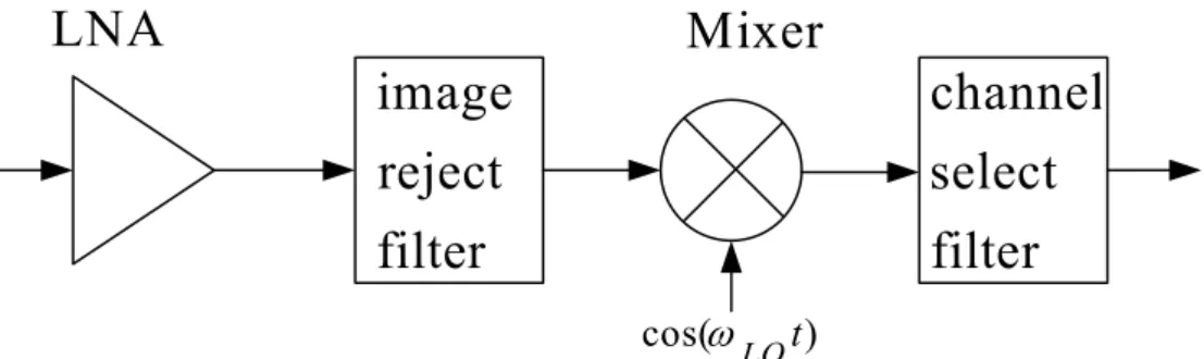
In heterodyne architectures, the signal band is translated into much lower frequencies by down-conversion mixer, and the filters are used to select the band and channel of the interested signals. In general, the low noise amplifier is placed in front of the down-conversion mixer, since the noise of the down-conversion mixer is high. A simple heterodyne architecture is shown in Fig. 2.1. This architecture is the most reliable reception technique today. But if the cost, complexity, integration and power dissipation are the primary criteria, the heterodyne receiver will become unsuitable due to its complexity and the need for a large number of external components.
Frequency planning is an important thing in heterodyne receiver. For high-side injection, an undesired signal (image) at a frequency of
) ( LO RF LO
IM ω ω ω
ω = + − is translated into the same frequency, intermediate frequency (IF), as the desired signal. Similarly, for low-side injection, the image
) cos(ωLOt
Mixer
filter
reject
image
filter
select
channel
LNA
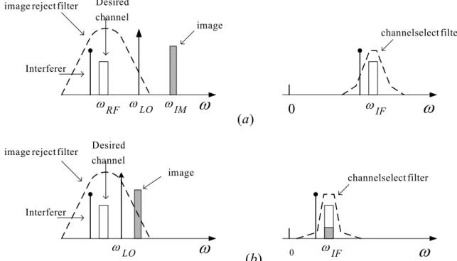
frequency is at ωIM =ωLO −(ωRF −ωLO). Therefore the image would cause the distortion of the signal at the intermediate frequency. As shown in Fig. 2.2, some techniques are necessary to suppress the image, such as image reject filter. How to choose the intermediate frequency? If 2ωIF is sufficiently large, the image reject filter will have a relatively small loss in the signal band and a large attenuation in the image band. But a lower 2ωIF will release the quality factor of the channel select filter to get great suppression of nearby interferers. Therefore we must take a trade-off between image rejection and channel selection.
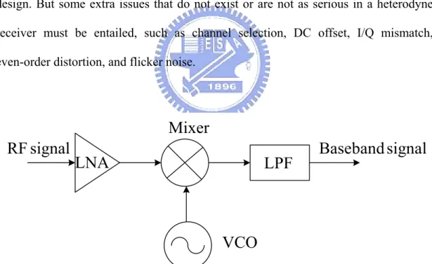
2.1.2 Homodyne Receiver
The homodyne receiver is also called “direct-conversion” or “zero-IF” architecture, since the RF signal is directly down-converted to the baseband in the first downconversion. In the homodyne receiver, the LO frequency is equal to the
0 0
ω
ω
ω
ω
LO ω LO ω channel Desired channel Desired Interferer Interferer image image filter reject image filter reject image filter select channel filter select channel IF ω IF ω ) (a ) (b IM ω RF ωFigure 2.2 Rejection of image versus suppression of interferers for (a) large ωIF (b) small ωIF
relatively sharp cutoff characteristics. The simple homodyne architecture is shown in Fig. 2.3. But quadrature outputs are needed for frequency and phase-modulated signals, since the two sides of FM or QPSK spectra carry different information. In recent years, this architecture becomes the topic of active research gradually due to the following reasons:
(1) The problem of image is removed due to ωIF = . Therefore no image filter is 0 required, and the LNA need not drive a 50-Ω load.
(2) It is attractive for monolithic integration because this architecture needs less external components.
For the above reasons, this architecture is suitable for low-power and single-chip design. But some extra issues that do not exist or are not as serious in a heterodyne receiver must be entailed, such as channel selection, DC offset, I/Q mismatch, even-order distortion, and flicker noise.
2.2 Wireless Local Area Network
In recent years, wireless local area networks (WLANs) become an important role in our life gradually. Some standards were established to regulate the development of the
LNA
Mixer
LPF
VCO
signal
RF
Baseband
signal
WLNAs. A brief introduction of our application is listed below:
IEEE 802.11a
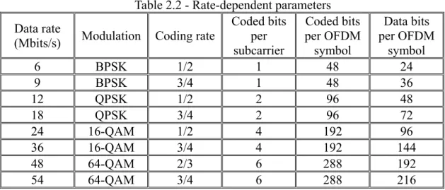
The IEEE 802.11a standard was defined by the Institute of Electrical and Electronics Engineers in 1999. The channelization scheme for this standard is shown in Table 2.1 and Fig. 2.4, and its physical layer is based on a 52 sub-carriers orthogonal frequency division multiplexing (OFDM) modulation scheme.
Table 2.1 - The set of the channelization
Regulatory domain Band Channel center frequencies United States U-NII lower band5.15-5.25 (GHz) 5180 MHz, 5200 MHz 5220 MHz, 5240 MHz United States U-NII middle band5.25-5.35 (GHz) 5260 MHz, 5280 MHz 5300 MHz, 5320 MHz United States U-NII upper band
5.725-5.825 (GHz)
5745 MHz, 5765 MHz 5785 MHz, 5805 MHz
This OFDM system provides a wireless LAN with data payload communication capabilities of 6, 9, 12, 18, 24, 36, 48, 54 Mbits/s, and its rate-dependent modulation parameters is shown in Table 2.2.
5180 5200 5220 5240 5260 5280 5300 5320
5150 5350
Edge Band
Lower Upper BandEdge
Spacing MHz 20 MHz/ 200 in Carriers 8 : Bands NII U Middle and Lower 5725 5745 5765 5785 5805 5825 Edge Band
Lower Upper BandEdge
MHz 30 MHz 30 MHz 20 MHz 20 Spacing MHz 20 MHz/ 100 in Carriers 4 : Bands NII -Upper U
Table 2.2 - Rate-dependent parameters Data rate
(Mbits/s) Modulation Coding rate
Coded bits per subcarrier Coded bits per OFDM symbol Data bits per OFDM symbol 6 BPSK 1/2 1 48 24 9 BPSK 3/4 1 48 36 12 QPSK 1/2 2 96 48 18 QPSK 3/4 2 96 72 24 16-QAM 1/2 4 192 96 36 16-QAM 3/4 4 192 144 48 64-QAM 2/3 6 288 192 54 64-QAM 3/4 6 288 216
For a NF of 10 dB and 5 dB implementation margins, the minimum input levels are shown in Table 2.3, and the maximum input power level is -30 dBm.
Table 2.3 – Receiver performance requirements Data rate
(Mbits/s) sensitivity (dBm) Minimum Adjacent channel rejection (dB) channel rejection (dB)Alternate adjacent
6 -82 16 32 9 -81 15 31 12 -79 13 29 18 -77 11 27 24 -74 8 24 36 -70 4 20 48 -66 0 16 54 -65 -1 15
2.3 Noise Basic
Noise can be loosely defined as any random interference unrelated to the signal of interest, and noise is characterized by a PDF and a PSD. In analog circuits, the signal-to-noise ratio (SNR), defined as the ratio of the signal power to the total noise power, is an important parameter. But in RF design, most of the front-end receiver blocks are characterized in terms of their noise figure, which is a measure of SNR degradation due to the added noise from the circuit/system, rather than the input-referred noise. Noise factor can be expressed as
source input to due power noise output power noise output total factor noise = (2-1)
the noise figure (NF) is simply the noise factor expressed in decibels. If a system has no noise, then noise figure is 0 dB regardless of the gain. In reality, the finite noise of a system degrades the SNR, yielding noise figure > 0 dB. For those whose noise factor is quite close to unity, noise temperature, TN, is an alternative way of
expressing the effect of noise contribution due to its higher-resolution description of noise performance, and is defined as the increase in temperature required of the source resistance for it to account for all of the output noise at the reference temperature Tref (which is 290 K). It is related to the noise factor as follows:
1) -factor (noise T T T T 1 factor noise N ref ref N ⇒ = ⋅ + = (2-2)
2.3.1 Noise Source
Thermal noise:Thermally agitated charge carriers in a conductor constitute a randomly varying current that gives rise to a random voltage due to their Brownian motion. Thermal noise is often called Johnson noise or Nyquist noise. The noise voltage has a zero average value, but a nonzero mean-square value.
In a resistor R, thermal noise can be represented by a series noise voltage source 2 4
n
v = kTR f∆ or by a shunt noise current source 2 4
n kT f i R ∆ = , where k is
Boltzmann’s constant (about 1.38×10⁻²³ J/K), T is the absolute temperature in Kelvins,
and Δf is the noise bandwidth. However, purely reactive elements generate no thermal noise.
(1) There must be direct current flow.
(2) There must be energy barrier over which a charge carrier hops.
Charge comes in discrete bundles. The randomness of the arrival time gives rise to the whiteness of shot noise. Therefore the shot noise can be modeled by a shunt noise current source 2 2
n DC
i = qI ∆ , where q is the electronic charge, If DC is the DC current
in amperes, and ∆f is the noise bandwidth in hertz. Flicker Noise:
Flicker noise appears as 1/f character and is found in all active devices, as well as in some discrete passive element such as carbon resistors. In diodes, flicker noise is caused by traps associated with contamination and crystal defects in the depletion regions. The traps capture and release carriers in a random fashion and the time constants associated with the process give rise to the 1/f nature of the noise power density. The flicker noise in diode can be represented as 2
j j K I i f f A = ⋅ ⋅ ∆ , where K is the process-dependent constant, Aj is the junction area, and I is the bias current. In
MOSFET, charge trapping phenomena are invoked in surface, and his type of noise is much greater than that of the bipolartransistor. The flicker noise in MOSFET can be given by 2 2 2 2 m n T ox g K K i f A f f WLC f ω = ⋅ ⋅ ∆ ≈ ⋅ ⋅ ⋅ ∆ (2-3)
where K is the process-dependent constant and A is the area of the gate.
2.3.2 Noise Model of MOSFET
The dominant noise source in CMOS devices is channel noise, which basically is thermal noise originated from the voltage-controlled resistor mechanism of a MOSFET. This source of noise can be modeled as a shunt current source in the output
circuit of the device. The channel noise of MOSFET is given by f
g kT
ind2 =4 γ d0∆ (2-4)
where γ is bias-dependent factor, and gd0 is the zero-bias drain conductance of the device. Another source of drain noise is flicker noise and is given by (2-3). Hence, the total drain noise source is given by
f WLC g f K f g kT i ox m d nd = ∆ + ⋅ 2 ⋅∆ 2 0 2 4 γ (2-5)
At RF frequencies, the thermal agitation of channel charge leads to a noisy gate current because the fluctuations in the channel charge induce a physical current in the gate terminal due to capacitive coupling. This source of noise can be modeled as a shunt current source between gate and source terminal with a shunt conductance gg,
and may be expressed as f
g kT
ing2 =4 δ g∆ (2-6)
where the parameter gg is shown as
0 2 2 5 d gs g g C g =ω (2-7)
and δ is the gate noise coefficient. This gate noise is partially correlated with the channel thermal noise because both noise currents stem from thermal fluctuations in the channel, and the magnitude of the correlation can be expressed as
j i i i i c d g d g 395 . 0 2 2 * − ≈ ⋅ ⋅ ≡ (2-8)
where the value of -0.395j is exact for long channel devices. Hence, the gate noise can be re-expressed as ) | | 1 ( 4 | | 4 ) ( 2 2 2 2 i i kT g f c kT g f c ing = ngc + ngu = δ g∆ + δ g∆ − (2-9)
where the first term is correlated and the second term is uncorrelated to channel noise. From previous introduction of MOSFET noise source, a standard MOSFET noise model can be presented in Fig. 2.5, where 2
nd
i is the drain noise source, 2
ng
i is the gate noise source, and 2
rg
v is thermal noise source of gate parasitic resistor r . g
2.3.3 Noise Figure of Cascaded Stages
For a cascade of m stages, the overall noise figure can be characterized by Friis formula ) 1 ( 1 2 1 1 ... 1 ) 1 ( 1 − − + + − + − + = m p m p total A NF A NF NF NF (2-10)
where NF is the noise factor of stage n, and n A denotes the power gain of pn stage n. This equation indicates that the noise contributed by each stage decreases as the gain preceding the stage increases. Hence, the first few stages in a cascade are the most critical for noise figure. But if a stage exhibits attenuation, then the noise figure of the following circuit is amplified when referred to the input of that stage.
2.4 Linearity Basic
The nonlinearity of the system often leads to interesting and important phenomena,
G
S
gsC
D
S
2 ngi
v
gsg
mv
gsr
oi
nd2 2 rgv
r
g-+
such as harmonics, gain compression, desensitization, blocking, cross modulation, intermodulation, etc. These distortions will degrade the performance of the system. Volterra series will be used for distortion computations. It can provide designers some information to derive which circuit parameters or circuit elements they have to modify in order to obtain the required specifications. Therefore, we introduce Volterra series in the section.
2.4.1 Fundamental of the Volterra Series
In fact a Volterra series describes a nonlinear system in a way which is equivalent to the way Taylor series approximate an analytic function. A nonlinear system which is excited by a signal with small amplitude can be described by a Volterra series which can be broken down after the first few terms. The higher the input amplitude, the more terms of that series need to be taken into account in order to describe the system behavior properly. For very high amplitudes, the series diverges, just as Taylor series. Hence, Volterra series are only suitable for the analysis of weakly nonlinear circuits.
The Volterra series approach has been proven to very attractive for hand calculations of small transistor networks. Since Volterra kernels retain phase information, they are especially useful for high-frequency analysis.
1
H
n
H
2
H
)
(t
x
y
(t
)
M
M
The theory of Volterra series can be viewed as an extension of the theory of linear, first-order systems to weakly nonlinear systems. And a system is considered as the combination of different operators of different order in the Volterra series description, as shown in Fig. 2.6. Every block H1, H2, and Hn represents an operator of order 1, 2,
and n, respectively. How much operators must be used is dependent on the input amplitude. In general, the weakly nonlinear effects can be described accurately by taking into account third-order effects only.
In the time domain, the transformation on an input signal, x(t), performed by a nth-order Volterra operator is given by
∫
∫
−+∞∞ +∞ ∞ − − − − = n n n n n x t h x t x t x t d d d H [ ( )] L (τ1,τ2,L,τ ) ( τ1) ( τ2)L ( τ ) τ1 τ2L τ (2-11) the n-dimension integral is seen to be an nth-order convolution integral. The function) , , , ( 1 2 n n
h τ τ Lτ is an nth-order Volterra kernel. The output of a nonlinear system can be represented as the sum of the output of a first-order Volterra operator with the output of a second-order one, a third-order one, and so on, as shown in Fig. 2.6. The Volterra series representation of the nonlinear system can be expressed as
)] ( [ )] ( [ )] ( [ )] ( [ ) (t H1 x t H2 x t H3 x t H x t y = + + +L+ n (2-12)
In the frequency domain, the nth-order Volterra kernel can be given by
∫
∫
−+∞∞ + + − +∞ ∞ − = s s n n n n n s s h e d d d H L L τ L τ τ L nτn τ τ L τ 2 1 ) ( 1 1, , ) ( , , ) 11 ( (2-13)and is called the nth-order nonlinear transfer function or the nth-order kernel transform.
2.4.2 Nonlinear Performance Parameters in Terms of Volterra Kernels
When a system that can be described by a Volterra series up to order three, is excited by the sum of two sinusoidal excitations A1cosω and 1t A2cosω , then the 2t output is given by the sum of the responses listed in Table 2.4. From Table 2.4, theTable. 2.4 Different responses at the output of a nonlinear system described by Volterra kernels.
Order Frequency of response Amplitude of response Type of response 1 1 1 ω 2 ω ) ( 1 1 1H jω A ) ( 2 1 2 H jω A Linear 2 2 2 1 ω ω + | |ω1−ω2 ) , ( 1 2 2 2 1A H jω jω A ) , ( 1 2 2 2 1A H jω jω A − 2nd-order intermodulation products 2 2 1 2ω 2 2ω 2 1 ( , ) 1 1 2 2 1 H jω jω A 2 1 ( , ) 2 2 2 2 2 H jω jω A 2nd harmonics 2 2 0 0 2 1 ( , ) 1 1 2 2 1 H jω jω A − 2 1 ( , ) 2 2 2 2 2 H jω jω A − DC shift 3 3 3 3 2 1 2ω +ω | 2 | ω1−ω2 2 1 2ω ω + | 2 |ω1− ω2 4 3 ( , , ) 2 1 1 3 2 2 1 A H jω jω jω A 4 3 ( , , ) 2 1 1 3 2 2 1 A H jω jω jω A − 4 3 ( , , ) 2 2 1 3 2 2 1A H jω jω jω A 4 3 ( , , ) 2 2 1 3 2 2 1A H jω jω jω A − − Third-order intermodulation products 3 3 1 2 2 1 ω ω ω ω + − = 2 2 1 1 ω ω ω ω − + = 4 3 ( , , ) 2 2 1 3 2 2 1A H jω jω jω A − 4 3 ( , , ) 2 1 1 3 2 2 1 A H jω jω jω A − Third-order desensitization 3 3 1 1 1 2ω −ω =ω 2 2 2 2ω −ω =ω 4 3 ( , , ) 1 1 1 3 3 1 H jω jω jω A − 4 3 ( , , ) 2 2 2 3 3 2 H jω jω jω A − Third-order compression or expansion 3 3 1 3ω 2 3ω 4 1 ( , , ) 1 1 1 3 3 1 H jω jω jω A 4 1 ( , , ) 2 2 2 3 3 2 H jω jω jω A Third harmonics
expressions for the second and third harmonic distortion in terms of general Volterra are given by ) ( ) , ( 2 1 1 1 1 2 1 2 ω ω ω j H j j H A HD = (2-14) ) ( ) , , ( 4 1 1 1 1 1 3 2 1 3 ω ω ω ω j H j j j H A HD = (2-15)
Furthermore, among the intermodulation products, the third-order intermodulation products at 2ω1−ω2 and 2ω2 −ω1 is important. Since if the difference between
1
ω and ω is small, the distortions at 2 2ω1−ω2 and 2ω2 −ω1 will appear in the vicinity of ω and 1 ω . Using Table 2.4 the third-order intermodulation distortion in 2
terms of Volterra kernel transforms
) ( ) , , ( 4 3 1 1 2 2 1 3 2 2 3 ω ω ω ω j H j j j H A IM = − (2-16)
This effect causes some distortion at our desired frequency and damages desired signals. Therefore third intercept point (IP3) is used to characterize this behavior. This parameter is measured by supplying a two-tone signal to the system. This input signal must be chosen to be sufficiently small in order to remove higher-order nonlinear terms. In a typical test, A1=A2=A, hence the magnitude of third-order intermodulation
products grows at three times the rate at which the fundamental signal on a logarithmic scale when input signal increases. The third-order intercept point is defined to be the point at which third-order intermodulation product equals to the fundamental signal, and the corresponding input signal is called input IP3 (IIP3) and the corresponding output signal is called output IP3 (OIP3). The AIP3, therefore, can be obtained by setting IM3 =1 and expressing as
) , , ( ) ( 3 4 2 2 1 3 1 1 2 3 ω ω ω ω j j j H j H AIP − = (2-17)
Besides, a quick method of measuring IIP3 is as follows. As shown in Fig. 2.7, If the power of the two-tone signal, Pin, is small enough to ignore higher order nonlinear
terms, then IIP3 can be expressed as
dBm in dB dBm P P IIP | 2 | | 3 + ∆ = (2-18) P ∆ 2 P ∆ 2 3 P∆ 3 IIP 3 OIP in P input power(dBm) power(dBm) output ω 1 ω ω2 2 1 2ω −ω 2ω2−ω1 P ∆ 1 slop signal l fundamenta = 3 slop IM3 = signal l fundamenta IM3 (a) (b)
Figure 2.7 (a) Growth of output components in an intermodulation test (b) Intermodulation distortion
CHAPTER 3
Design Consideration in Front-End Circuit Design
3.1 Low Noise Amplifier Basic
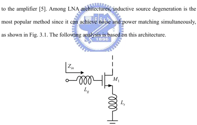
Low noise amplifier is the first gain stage in the receive path so its noise figure directly adds to that of the system. There, therefore, are several common goals in the design of LNA. These include minimizing noise figure of the amplifier, providing enough gain with sufficient linearity and providing a stable 50 Ω input impedance to terminate an unknown length of transmission line which delivers signal from antenna to the amplifier [5]. Among LNA architectures, inductive source degeneration is the most popular method since it can achieve noise and power matching simultaneously, as shown in Fig. 3.1. The following analysis is based on this architecture.
3.1.1 Low Noise Amplifier Architecture Analysis
In Fig. 3.1, the input impedance can be expressed asin Z s L g L 1 M
gs s g o s T s gs m s gs m gs s g in C L L at L L C g L C g sC L L s Z ) ( 1 1 ) ( + = = ≈ = + + + = ω ω ω (3-1)
As shown in (3-1), the input impedance is equal to the multiplication of cutoff frequency of the device and source inductor at resonant frequency. Therefore it can be set to 50 Ω for input matching while resonant frequency is designed to be equal to the operating frequency.
According to prior introduction, the equivalent noise model of common-source LNA with inductive source degeneration can be expressed as Fig. 3.2, where R is l
the parasitic resistance of the inductor, Rg is the gate resistance of the device. Note
that the overlap capacitance Cgd has also been neglected in the interest of simplicity.
Then the noise figure can be obtained by computing the total output noise power and output noise power due to input source. To find the output noise, we first evaluate the transconductance of the input stage. With the output current proportional to the voltage on Cgs and noting that the input circuit takes the form of series-resonant
network, the transconductance at the resonant frequency can be expressed as
s o T s T s gs o m in m m R L R C g Q g G ω ω ω ω ( + ) = 2 = = (3-2) gs C 2 ngu i vgs gmvgs ind2 2 Rg v -+ 2 ngc i g R l R g L s L s R 2 Rl v 2 s v 2 out i
where Qin is the effective Q of the amplifier input circuit. So the output noise power
density due to the source can be expressed as
2 2 2 2 . , ) 1 ( 4 ) ( s s T s o T eff m Rs o Rs a R L R kT G S S ω ω ω ω + = = (3-3)
In the similar way, the output noise power density due to Rg and Rl is
2 2 2 2 , , ) 1 ( ) ( 4 ) ( s s T s o T l g o R R a R L R R R kT S g l ω ω ω ω + + = (3-4)
Furthermore, channel current noise of the device is the dominant noise contributor, and its noise power density associated with the correlated portion of the gate noise can be expressed as 2 , , ) 1 ( 4 ) ( s s T do o i i a R L g kT S ngc nd ω γκ ω + = (3-5)
where γ is the coefficient of channel thermal noise, α = gm/gd0 and
2 2 2 5 2 1 5 + + = γ δα γ δα κ c cQL (3-6) gs s o L C R Q ω 1 = (3-7)
The last noise term is the contribution of the uncorrelated portion of the gate noise, and its output noise power density can be expressed as
2 , ) 1 ( 4 ) ( s s T do o i a R L g kT S ngu ω ωγξ + = (3-8) where ) 1 )( 1 ( 5 2 2 2 L Q c + − = γ δα ξ (3-9)
According to (3-3), (3-4), (3-5) and (3-8), the noise figure at the resonant frequency can be expressed as + + + = T o L s g s l Q R R R R F ω ω α γχ 1 (3-10) where ) 1 ( 5 5 | | 2 1+ c QL 2 + 2 +QL2 = γ δα γ δα χ (3-11)
From (3-11), we observe that χ includes the terms which are constant, proportional to QL, and proportional to 2
L
Q . It follows that (3-11) will contain terms which are proportional to QL as well as inversely proportional to QL. A minimum
noise figure, therefore, exits for a particular QL.
3.1.2 Optimizations of Low Noise Amplifier Design Flow
The analysis of the previous section can now be drawn upon in designing the LNA. In order to pick the appropriate device size and bias point to optimize noise performance given specific objectives for gain and power dissipation, a simple second-order model of the MOSFET transconductance can be employed which accounts for high-field effects in short channel devices. Assuming that the drain current, Id, has the form
ρ ρ + = − + − = 1 1 ) ( 2 sat sat ox T gs sat T gs sat ox DS WC v LE V V LE V V v WC I (3-12) where sat T gs LE V V − ≡
ρ . And the (3-7) can be replace as
WL Q R C R WLC Q o L s ox s ox o L = 2ω 3 ⇒ = 2 3ω (3-13)
ρ ρ ω + = = 1 1 2 3 2 sat sat o s L DD DS DD D v E R Q V I V P (3-14)
The noise figure can be expressed in terms of PD and Vgs. Two parameters linked to
power dissipation need to be accounted for. ) ( 1 gs gs m T f V C g = ≈ ω (3-15) ) , ( 1 1 2 3 2 2 2 D gs D o s o D sat sat DD L P f V P P R P E v V Q = + = + = ρ ρ ρ ρ ω (3-16) where s o sat sat DD o R E v V P ω 2 3 = .
The noise figure of the LNA, therefore, can be expressed as
) , ( ) 1 ( 5 5 | | 2 1 1 2 2 2 D gs L L T o L s g s l c Q Q f V P Q R R R R F = + + + + + + = γ δα γ δα ω ω α γ (3-17)
In general, there are two approaches to optimize noise figure. The first approach assumes a fixed transconductance, Gm. The second approach assumes fixed power
consumption.
(1) Fixed Gm optimization: To fix the value of the transconductance, Gm, we need
only assign a constant value to ρ. Once ρ is determined, the optimization of the noise figure can be obtained by (3-17):
) , ( 0 ) , ( . .
.opt Lopt gs Dopt D Vgs fixed D D gs P V f F Q P P P V f = ⇒ ⇒ ⇒ = ∂ ∂ (3-18)
From (3-13), we can obtain the optimal width to get the minimal noise figure for a given Gm under the assumption of matched input impedance. In this approach, the
designer can achieve high gain and low noise performance by selecting the desired transconductance, but its disadvantage is that we must sacrifice the power consumption to achieve minimum noise figure.
(2) Fixed PD optimization: An alternative method of optimization fixes the power
dissipation and adjusts device size and bias point to minimize the noise figure. Once PD is determined, the optimization of the noise figure can be obtained by
(3-19): ) , ( 0 ) , ( . .
.opt Lopt gsopt D gs P fixed gs D gs P V f F Q V V P V f D = ⇒ ⇒ ⇒ = ∂ ∂ (3-19)
Then the optimum device size can be obtained to get the best noise performance for fixed power dissipation. In this approach, the designer can specify the power dissipation and find the optimal noise performance, but its disadvantage is that the transconductance is held up by the optimal noise condition.
3.2 Phase Splitter Basic
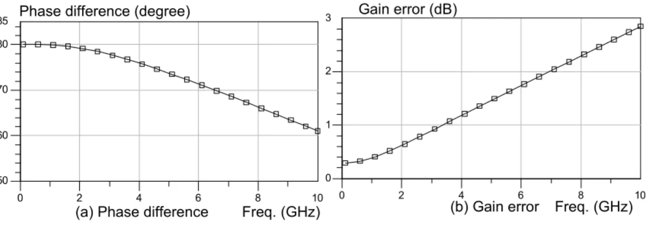
Differential phase splitters are basic cells required in microwave components such as balanced mixers, multipliers, and phase shifters. An ideal differential phase splitter will generate a 180 degree phase difference at its two outputs and the same magnitude of the power at each output from a single input [16].
In RFIC, there are passive and active differential phase splitters. The passive differential phase splitters can be achieved by using the LC networks or microstriplines. But the spiral inductors, MIM capacitors, and microstriplines are too expensive due to their larger physical size at lower microwave frequencies. Besides, the passive differential phase splitters may cause some signal loss. There are three categories of active differential phase splitters normally employed in lower microwave frequencies for wireless communications: single FET circuits, common-gate common-source circuits, and differential amplifier circuits. The
therefore the following introduction is based on this architecture.
The differential amplifier circuit is shown in Fig. 3.3. Ideally, this circuit will provide equal amplitude and 180 degree phase difference. However, the finite impedance at node x caused by strong parasitic at high frequency will affect the phase difference and gain balance of the circuit.
Now, we assume that the common source input impedance of M1 and M2 equals Z. The input ac signal vin can be expressed as
2 1 gs gs
in v v
v = − (3-20)
and the vgs1 and vgs2 have the following relation as
Z R R Z Z R v v source source source gs gs + = = − // 1 2 (3-21)
where Rsource is the input impedance of the current source.
In practice, the value of the Rsource is finite. This will cause that |vgs1|>|vgs2 | and
their phase difference is not 180 degree. The output signal, therefore, will not balance,
M1
M2
x
LR
R
L out1V
V
out2input
VDD
as shown in Fig. 3.4. To overcome this problem, some compensation method must be used.
To let the magnitude of the vgs1 and vgs2 be equal and the phase difference of the vgs1
and vgs2 equals 180 degree, a RC feedback circuit shown in Fig. 3.5 can be used to
compensate phase error [15]. The phase difference between input port and output port can be expressed as ) ( tan 90 1 RCω PhaseShift = − − (3-22) So we can obtain a desirable phase shift at the desired frequency by choosing proper value of R and C.
Fig. 3.6 shows the schematic of the phase splitter with RC compensation. The current source is realized by an active device. R1 and R2 are used to bias the
Phase difference (degree)
Freq. (GHz) Freq. (GHz) Gain error (dB)
(a) Phase difference2 4 6 8 (b) Gain error
0 10 160 170 180 150 185 2 4 6 8 0 10 1 2 0 3
Figure 3.4 Simulated results of Fig. 3.3 (a) phase difference (b) gain error
in
v
R
C
v
out
3.5. The resistor, Rf, is used to compensate the gain error. The relation between the vd1
and vg2 can be expressed as
f f eq eq d g R C Z R Z R v v + + = ω / 1 ) // ( // 1 1 1 2 (3-23)
where Req =R1// R2 and Z1 is the input impedance of M2 . The vg2, therefore, can
be adjusted by changing the value of Req, Cf, Rf, and Z1. The phase error can be
compensated by proper selection of Req and Cf, and the gain balance is achieved by
adjusting the value of Req, Cf, Rf, and Z1.
3.3 Down-Conversion Mixer Basic
The purpose of the mixer is to convert a signal from one frequency to another. In a receiver, this conversion is from radio frequency to intermediate frequency or zero-IF. Mixing requires a circuit with a nonlinear transfer function, since nonlinearity is
out1
V
V
out2 LR
R
Linput
M1
M2
1R
2R
1R
2R
VDD
fR
fC
fundamentally necessary to generate new frequencies. Fig. 3.7 shows a simplified CMOS Gilbert Cell mixer, which is composed of transconductance stage and switching stage.
The RF input must be linear, or adjacent channels could intermodulate and interfere with the desired channel. And the third-order intermodulation term from the two other signals will be directly on top of the desired signal. The LO input need not be linear, since the LO is clean and of known amplitude. In fact, the LO input is usually designed to switch the upper quad so that for half the cycle M3 and M6 are on and taking all current to output loading. For the other half of the LO cycle, M3 and M6 are off and M4 and M5 are on. This stage will be, therefore, like switch to mixing RF signal to IF signal.
3.3.1 Conversion Gain
The gain of mixers must be carefully defined to avoid confusion. The voltage
+
RF
RF
−
+
IF
IF
−
+
LO
LO
+
−
LO
VDD
VDD
M1
M2
M3
M4
M5 M6
LR
R
Lconversion gain of a mixer is defined as the ratio of the rms voltage of the IF signal and rms voltage of the RF signal. Note that the frequencies of these two signals are different. The power conversion gain of a mixer is defined as the IF power delivered to the load divided by the available RF power from the source. If the impedances are both matched to 50 Ω, then the voltage conversion gain and power conversion gain of the mixer are equal when they are expressed in decibels.
Now, we assume that M3-M6 work like an ideal switch, and the conversion transconductance of the mixer can be expressed as
m c g G π 2 = (3-24)
where gm is the transcondcutanc of M1 and M2, and 2/π is produced by switching stage.
3.3.2 Switching Stage
For small LO amplitude, the amplitude of the output depends on the amplitude of the LO signal. Thus, gain is larger for larger LO amplitude. For Large LO signals, the upper quad switches and no further increase occur. Thus, at this point, there is no longer any sensitivity to LO amplitude. Besides, if upper quad transistors are alternately switched between completely off and fully on, the noise will be minimized. Since upper transistor contributes no noise when it is fully off, and when fully on, the upper transistor behaves like a cascode transistor which does not contribute significantly to noise.
The large LO signal is required to let upper quad transistors achieve complete switching. But if the LO voltage is made too large, a lot of current has to be moved into and out of the transistors during transitions. This can lead to spikes in the signals and can actually reduce the switching speed and cause an increase in LO feed-through.
Thus, too large a signal can be just as bad as too small a signal.
3.3.3 Mixer Noise
Noise figure for a mixer is defined as
source input to due IF at power noise output IF at the power noise output total factor noise = (3-25)
In general, the noise figure of the mixer is divided to two categories, single-sideband (SSB) noise figure and double-sideband (DSB) noise figure. The difference between the two definitions is the value of the denominator in (3-25). In the case of SSB noise figure, only the noise at the output frequency due to the source that originated at the RF frequency is considered, and it is usually used in heterodyne systems. In the case of DSB noise figure, all the noise at the output frequency due to the source is considered (noise of the source at the input and image frequencies), and it is usually used in homodyne systems.
Because of the added complexity and the presence of noise that is frequency translated, mixers tend to be much noisier than LNAs. In generally, mixers have three frequency bands where noise is important:
(1) Noise already presents at the IF: The transistors and resistors in the circuit will generate noise at the IF. Some of this noise will make it to the output and corrupt the signal.
(2) Noise at the RF and image frequency: The noise presents at the RF and image frequency will be mixed down to the IF.
(3) Noise at multiples of the LO frequencies: Any noise that is near a multiple of the LO frequency can also be mixed down to the IF, just like the noise at the RF. Besides, the flicker noise will become more important in the homodyne receiver. In the design of the direct down-conversion mixer, how to reduce the flicker noise of
upper quad transistors is the important thing. According to (2-3), this noise can be reduced by increasing the device size for a given gm.
3.3.4 Port-to-Port Isolation
The isolation between each two ports of a mixer is critical. The LO-RF feed-through results in LO leakage to the LNA and eventually the antenna, whereas the RF-LO feed-through allows strong interferers in the RF path to interact with the local oscillator driving the mixer. The LO-IF feed-through is important because if substantial LO signal exists at the IF output even after low-pass filtering, then the following stage may be desensitized. Fortunately, this feed-through can be reduced largely by used the double-balanced architecture. Finally, the RF-IF isolation determines what fraction of the signal in the RF path directly appears in the IF, a critical issue with respect to the even-order distortion problem in homodyne receivers. The required isolation levels greatly depend on the environment in which the mixer is employed. If the isolation provided by the mixer is inadequate, the preceding or following circuits may be modified to remedy the problem.
3.3.5 Linearity
As far as cascaded stages are concerned, linearity is a very important performance in mixer stage. In general, it will dominate the distortion of the entire receiver. The detail analysis will be introduced in Chapter 4.
CHAPTER 4
5.5 GHz Low-Power and High-Linearity Mixer
The mixer is based on the conventional doubly balanced CMOS Gilbert Cell mixer, as shown in Fig. 3.7 and it is composed of transconductance stage, mixing stage, load impedance and current source. The doubly balanced configuration exhibits following advantages:
(a) It generates less even-order distortion resulted from transconductance stage.
(b) It has less LO-IF feed-through. Because the differential pairs M3-M4 and M5-M6 add the amplified LO signal with opposite phases, thereby providing a first-order cancellation.
4.1 Low-Power Design Consideration
Since each of conducting MOSFETs are ideally in saturation, the expected drain to source voltage is VT +200mV , neglecting body effect. Consequently, this architecture needs at least 3VT +600mV . This high voltage is not suitable for low-power design therefore we adopt following techniques to reduce supply voltage.
4.1.1 Low Voltage Topology
In order to reduce supply voltage, we adopt a typical low-voltage topology shown in Fig. 4.1(a). This topology uses two RF traps and one coupling capacitor. The function of the RF traps is provide a low impedance across its terminals at dc and high impedance at RF, and the function is usually realized by using on-chip LC tanks. The function of the coupling capacitor is used to couple the RF energy between the two
elements. Therefore the dc equivalent circuit becomes two independent biasing paths, as shown in Fig. 4.1(b), and the function of the ac equivalent circuit is the same as that of the cascode topology [3]. So this topology can achieve following advantages: (a) Lower supply voltage.
(b) The property of the cascode topology is retained.
(c) The two paths can be biased at different bias condition based on the different consideration.
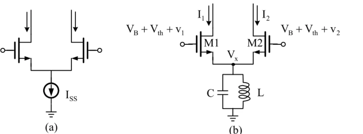
4.1.2 Narrowband Source-Coupled Pair
As shown in Fig. 4.2 (a), the first stage of the Gilbert cell mixer is the source-coupled pair transconductance stage. The high impedance of the current source forces the output currents to be balanced when input signal is unbalanced. On the other hand, if the input signal is perfectly differential, the output current is also balanced. The architecture is unsuitable for low-power design since the current source needs at least VT +200mV . In some cases, the current source is removed to reduce
rail bias Bottom rail bias Top rail bias Top rail bias Bottom elem ent1 elem ent2 el em ent1 elem ent2 elem ent2 ele m en t1 trap RF trap RF GND AC GND AC pass by circuit equivalent DC ACequivalentcircuit (a) (b) (c) Figure 4.1 Low-voltage topology
supply voltage, but the drawback of the omission is that the mixer will not reject unbalance in the RF differential inputs. Therefore we adopt a LC tank to replace the conventional current source, as shown in Fig. 4.2 (b). In dc biasing condition, the inductor provides a low resistance path for the dc bias current of M1 and M2 to ground, hence it almost needs no dc voltage drop across the source-coupled pair. At the operating frequency, the high impedance of the tank exhibits the ac function of the current source when the resonance frequency of the tank is tuned at ω0 (i.e.,
2 0 /
1 LC =ω ).
The detail analysis is as follows. In Fig. 4.2 (b), the current of the M1 and M2 can be expressed as 2 1 1 ( ) 2 B x n V v V K I = + − (4-1) 2 2 2 ( ) 2 B x n V v V K I = + − (4-2)
where K is the large signal transconductance parameter. The voltage n V of the x common-source node can be expressed as (4-3) by using Kirchoff’s current law
∫
+ = + Vxdt L dt dV C I I x 1 2 1 (4-3) M1 M2 L C x V 1 I I2 SS I 1 th B V v V + + VB +Vth +v2 (a) (b)Thus, from (4-1), (4-2) and (4-3), we can obtain (4-4) + + + + − = + + 2 ) 2 )( ( 1 2 2 2 2 1 2 1 2 2 v v V v v Vx V dt d C K Vx LC Vx dt d C g Vx dt d x B n m (4-4)
then the solution of the voltage V depends on the input signals, x v1 and v2.
In the case of a single-ended input signal (v1 = Asinω0t,v2 =0), the voltage V x can be expressed as ψ ω + = A t Vx sin 0 2 (4-5)
where ψ represents the solution of the nonlinear differential equation, (4-6), t A C K dt d V C g dt d n B m 0 2 0 2 0 2 2 2 sin 4 1 2 ψ ψ ω ψ ω ω ψ + = − + (4-6)
In equation (4-6), the ψ contain the harmonics of 2ω0 and maybe higher, but none at ω0.
In the case of a differential input signal (v1 =−v2 =(A/2)sinωot), the voltage V x can be expressed as
ψ
=
Vx (4-7)
and the solution can be verified in Fig. 4.3.
50 100 150 200 250 300 0 350 -10 -5 0 5 10 -15 15 50 100 150 200 250 300 0 350 -4 -2 0 2 4 -6 6 time (ps) time (ps) Voltage (mV) v1 v2 Vx Voltage (mV) v1 v2 Vx (a) (b)
As shown in Fig. 4.3, if the input signal is single-ended, the common-source terminals will have a voltage wave of 1/2 the input amplitude. On the other hand, the common-source terminals will exhibit no power at ω0 when input signal is
differential pair. Therefore the transconductance stage responds to difference between
1
v and v2. In other words, the common-mode gain is reduced by the LC tank. Besides, the differential output current can be expressed as
) sin( ) sin( 0 0 2 1 0 I I g A t K A t I = − = m ω − nψ ω (4-8)
In (4-8), the first term is the linear transform, and the second term is the distortion signals. Of particular interest is the third-order distortion term which is generated by multiplying the second-harmonics (2ω0) of the ψ and the sin(ω0t). Thus the low impedance at 2ω0 will cause lower second-harmonics and get better linearity than
that of the conventional current source.
4.2 Analysis of Linearity
In low-power RF transceiver design, linearity requirement becomes more and more challenging. Circuit nonlinearity results in various system distortions associated with the even- and odd-order nonlinearities. Of these distortions, the third-order intermodulation is one of the most critical terms responsible for linearity degradation in general RF systems. Due to the fact, how to improve the linearity of RF circuits without extra power consumption becomes an important topic to be studied.
As far as cascaded stages are concerned, system design calls for high linearity in the mixer stage to alleviate the distortion issues. A mixer is generally composed of a transconductance amplifier and a switching stage. Linearity is most limited by the transconductance amplifier, and therefore we will discuss the nonlinear effect of the
common-source amplifier in section 4.2.1.
In recent years, several techniques have been proposed to improve the linearity of MS/RF circuits by linearization of the nonlinear transconductance, such as degeneration feedback [5] and a bisymmetric Class-AB stage [6]. Another scheme is the superposition of auxiliary transistors operated in different bias conditions to null the derivative of device transconductance [7, 8]. Combined with the technique of out-of-band impedance termination, circuit linearity can be further enhanced, as indicated by the Volterra series analysis [9, 10]. The scheme, named as derivative superposition or multiple gated transistors (MGTR), offers a good opportunity to extend linearity without increasing power consumption, and is introduced in section 4.2.2.
Reference [10] gives designs showing that the device size of the auxiliary transistor (AT) is larger than that of the main transistor (MT), which does not precisely match to the derivative cancellation analysis derived through DC transconductance analysis. It is proposed that a complex transconductance shall be employed to search for the optimal design parameters. Therefore we propose a compact box-type equivalent circuit for the design of the multiple gated transistors technique in section 4.2.3.
4.2.1 Nonlinear Effects of Common-Source Amplifier
For the common-source amplifier, the nonlinear effect is dominated by the transconductance and the output conductance of the device. The nonlinear effects of the capacitances and substrate can be neglected, and they can be considered as linear elements [11]. Therefore we only consider the transconductance and the output conductance as the nonlinear source for the following analysis.
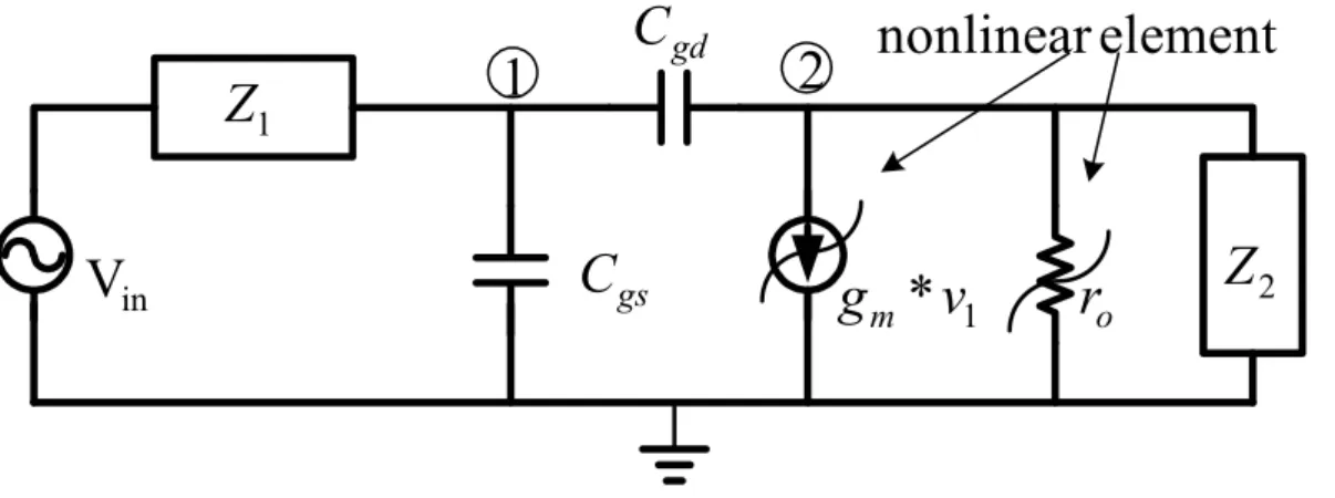
Fig. 4.4 shows a common-source amplifier, where Z1 is the input impedance, and Z2 is the output impedance. From the above-mentioned introduction and assuming that the common-source amplifier works in the weakly nonlinear region, the