鉍-銻-碲奈米線之合成、量測與熱電性質 - 政大學術集成
64
0
0
全文
(2) 摘要 諸多的研究顯示,和塊材相比,低維度的材料其物理性質會有所不同,為了 探究熱電材料在低維度下對其熱電性質所造成的效應,我們合成了 BixSb2-xTe3-y 奈米線並量測其熱電性質。本實驗藉由熱處理薄膜製備奈米線的方法合成單晶 BixSb2-x Te3-y 奈米線。我們先利用脈衝雷射沉積系統將 BixSb2-x Te3 鍍在矽基板上 形成薄膜,再將薄膜以 350 ℃至 490 ℃熱處理 5 到 21 天,奈米線即為了平衡因 薄膜與矽基板彼此熱膨脹係數不同所造成的應力而自薄膜上長出,其直徑為幾十 奈米至幾百奈米不等,長度則為幾微米至幾十微米。為了瞭解奈米線之構成與量. 政 治 大 加熱元件及溫度感測元件之量測平台上,由於奈米線已被架空,我們便能透過選 立 測其熱電性質,我們結合微影製程及操縱技術,將單根奈米線架空於附有電極、. ‧ 國. 學. 區繞射分析奈米線其結晶性,並使用能量散射分析儀得知奈米線之成分,利用四 點量測可得知奈米線的電阻率 ρ,以加熱元件在奈米線兩端產生溫差,並量測因. ‧. 西貝克效應 (Seebeck effect) 所造成之電壓差即能得到西貝克係數 S (Seebeck. sit. y. Nat. coefficient),三倍頻技術要求所量測的樣品必須要架空於基板上,運用三倍頻技. al. er. io. 術 (3ω method) 可量測奈米線之熱導率 κ 及比熱。結合微影製程、操縱技術以及. v. n. 量測系統,我們成功得到單根奈米線的三個熱電係數 ρ、S 以及 κ,並了解低維. Ch. 度對熱電性質所造成的影響。. engchi. i. i n U.
(3) Abstract Compare with the bulk materials, many researches had revealed that physical properties were different in low dimensional materials. To study the low-dimensional effects on thermoelectric properties of thermoelectric materials, BixSb2-xTe3-y nanowires were synthesized and studied for their thermoelectric properties. Single-crystallized BixSb2-xTe3-y nanowires were synthesized by on-film formation of nanowires. First, BixSb2-xTe3 thin films were deposited on SiO2/Si substrates by using the pulsed laser deposition system. BixSb2-xTe3-y nanowires grew from the films by. 政 治 大 between the film and the. annealing the films at 350~490 ℃ for 5~21 days through the stress release of the thermal expansion mismatch. 立. substrate. A series of. BixSb2-xTe3-y nanowires were prepared with the diameter from few tens of nanometers. ‧ 國. 學. to few hundreds of nanometers and the length from few micrometers to few tens of. ‧. micrometers. In order to analyze the components and measure the thermoelectric. sit. y. Nat. properties of the nanowires, the technique of combining microfabrication and. io. er. manipulation for suspending a single BixSb2-xTe3-y nanowire on a measurement platform with electrodes, heater and thermometers was developed. As long as the wire. al. n. v i n is suspended, the crystallizationC of the nanowire is able h e n g c h i Uto be analyzed by the selected. area electron diffraction (SAED). The composition of the nanowire can be analyzed by the STEM-EDX. Resistivity ρ is measured by the four-point probe method. In order to get the Seebeck coefficient S, temperature difference were generated by the heater and thermoelectric voltage generated by Seebeck effect were measured. The 3ω method which demands that the wire should be suspended was applied to measure the thermal conductivity κ and specific heat c. By using the developed technique and the measurement system, three thermoelectric parameter ρ, S, κ of a single nanowire were successfully measured and the low-dimensional effect on thermoelectric properties were examined. ii.
(4) 致謝 首先我想要感謝的是我的家人們,感謝我很愛很愛的媽媽和爸爸養育我,支 持我走到這一步,感謝我很愛很愛的妹妹和弟弟,我們相親相愛,互相扶持,做 哥哥的我真的很開心有你們這兩個小的,感謝我很愛很愛的阿公,謝謝你來參加 我的畢業典禮,看你穿上我的碩士袍後露出的笑容,讓我覺得一切的努力都是值 得的,第一次離開高雄到台北就學,心情既緊張又期待,感謝姑姑、姑丈還有表 兄弟姊妹們,讓我在外地求學時有個依靠。 感謝陳洋元教授既嚴謹又開放的指導,讓我在實驗上有所發揮並且往正確的. 政 治 大 能獨立完成奈米線的製作,還有熊德智學長在我實驗初期帶了我一陣子,讓我對 立 方向進行,感謝尚謙學長從我一進實驗室就開始帶著我做實驗直到他畢業,讓我. ‧ 國. 學. 奈米線的量測有初步的了解,非常非常感謝秉中學長,總是給我啟發,為我解惑, 在他的帶領下我學到了很多,讓我得以交出成果順利畢業,感謝虹蚚學長、翊誠. ‧. 學長、偉嘉學長在無塵室的製程幫我很多忙,正龍學長和天蔚學長總是不吝色地. sit. y. Nat. 給我們這些學弟妹們一些指教,我想我永遠不會忘記和政憲、育竹、耀文一起煮. al. er. io. 麵趕論文的那些日子,特別要感謝政憲在塊材的製作與量測上給我的幫助,感謝. v. n. 慈蓮學姊、佳華學長、Dedi、瀞謙、泓舜、暉閔、琬婷、怡臻、凡芸、寬仁學長. Ch. engchi. i n U. 和學弟妹們,因為有你們,奈米材料與低溫物理實驗室內總是充滿了歡笑聲,為 我的碩士生涯增添好多好多的樂趣,還要特別感謝中央研究院奈米核心設施中心 曾傳銘博士在 TEM 分析上的大力協助與郭白嘉學長代為操作 FIB,感謝在碩一 與我一起熬夜讀書、寫作業的同學們,特別感謝勛哥告訴我研發替代役的資訊, 讓我得以在智慧財產局服役。. iii.
(5) Table of Contents 摘要 .............................................................................................................................. i Abstract ....................................................................................................................... ii 致謝 ............................................................................................................................ iii Table of contents ....................................................................................................... iv List of figures ............................................................................................................. vi List of tables ............................................................................................................. xii. 政 治 大 Chapter 2 Thermoelectric立 material .......................................................................... 2 Chapter 1 Introduction ............................................................................................. 1. ‧ 國. 學. 2.1 Thermoelectric effect ......................................................................................... 2 2.2 Figure of merit .................................................................................................... 5. ‧. Chapter 3 Synthesis of nanowires ............................................................................ 7. sit. y. Nat. io. al. er. 3.1 Experimental equipment and techniques ............................................................ 8. v. n. 3.2 Target preparation ............................................................................................ 11. Ch. engchi. i n U. 3.3 Film deposition ................................................................................................. 14 3.4 Annealing process ............................................................................................ 17 3.5 Analysis results ................................................................................................ 20 Chapter 4 Thermoelectric property measurements of nanowires ...................... 28 4.1 Experimental equipment and techniques .......................................................... 28 4.2 Primary measurement platform fabrication ...................................................... 34 4.2 Nanowires suspension and completion of measurement platform ................... 34 4.4 Thermoelectric property measurements of nanowires ..................................... 41 iv.
(6) 4.4.1 Resistivity measurement ............................................................................ 41 4.4.2 Seebeck measurement ............................................................................... 41 4.4.3 Thermal conductivity measurement .......................................................... 42 4.4.4 Pattern design ............................................................................................ 43 4.5 Measurement results ......................................................................................... 45 Chapter 5 Conclusions ............................................................................................. 50 References ................................................................................................................. 51. 立. 政 治 大. ‧. ‧ 國. 學. n. er. io. sit. y. Nat. al. Ch. engchi. v. i n U. v.
(7) List of figures Chapter 2 Figure 2.1. The Seebeck effect ...................................................................... 2. Figure 2.2. The Peltier effect ........................................................................ 3. Figure 2.3. (a) The Seebeck circuit configured as a generator. (b) The Seebeck circuit configured as a cooler ....................................... 3. Figure 2.4. The Thomson effect .................................................................... 4. Figure 2.5. Schematic dependence of electrical conductivity, Seebeck. 政 治 大 concentration of free carriers ...................................................... 立. coefficient, power factor, and thermal conductivity on. ‧ 國. Figure 3.1. 學. Chapter 3. 5. Schematic representation of the growth of BiSxb2-xTe3. ‧. nanowires by stress-induce method. (a) Deposit BiSxb2-xTe3 thin. sit. y. Nat. films on SiO2/Si substrates by using pulsed laser deposition. io. al. er. system. (b) Seal the films in a vacuumed quartz tube. (c). n. Anneal the films at 350~500 ℃ for 5~21 days (d) Completion of BixSb2-xTe3. v i n C h growth ................................................ nanowires engchi U. 7. Figure 3.2. Scheme for X-ray diffraction ...................................................... 8. Figure 3.3. Pulsed laser deposition system for nanoparticles and thin film fabrication ................................................................................... 9. Figure 3.4. Exterior view of TEM and cross section of column ................... 10. Figure 3.5. X-Ray diffraction pattern of Bi0.5Sb1.5Te3 ingot ......................... 12. Figure 3.6. EDX spectrum of Bi0.5Sb1.5Te3 ingot .......................................... 12. Figure 3.7. X-Ray diffraction pattern of Bi1.5Sb0.5Te3 ingot ......................... 13. Figure 3.8. EDX spectrum of Bi1.5Sb0.5Te3 ingot .......................................... 13 vi.
(8) Figure 3.9. SEM image of Bi0.5Sb11.5Te3 thin film that deposited for 1 hour. The power and the frequency of the laser are 170mJ and 10Hz respectively. The rectangular shows the corresponding area of EDX analysis .............................................................................. 14. Figure 3.10. EDX spectrum of Bi0.5Sb1.5Te3 film ............................................ 15. Figure 3.11. AFM analysis shows that the thickness of the film is about 38nm ........................................................................................... 15. Figure 3.12. SEM image of Bi1.5Sb0.5Te3 thin film that deposited for 5 min.. 政 治 大 respectively. The rectangular shows the corresponding area of 立 The power and the frequency of the laser are 160mJ and 30Hz. EDX analysis .............................................................................. 16. ‧ 國. 學. EDX spectrum of Bi1.5Sb0.5Te3 film ............................................ 16. Figure 3.14. AFM analysis shows that the thickness of the film is about. ‧. Figure 3.13. y. sit. OM image of the Bi0.5Sb1.5Te3 thin film after annealing at. io. er. Figure 3.15. Nat. 88nm ............................................................................................. 17. 350 ℃ for 21 days .................................................................... 18. n. al. Figure 3.16. Ch. Side view SEM image of Bi0.5Sb1.5. engchi. v i n Te U film after annealing at 3. 350 ℃ for 21 days .................................................................... 18 Figure 3.17. OM image of the Bi1.5Sb10.5Te3 thin film after annealing at 490 ℃for 5 days ........................................................................ 19. Figure 3.18. Side view SEM image of Bi1.5Sb10.5Te3 film after annealing at 490 ℃ for 5 days ...................................................................... 19. Figure 3.19. SEM image of a suspend nanowire No.1 which grown from Bi0.5Sb1.5Te3 film after annealing at 500 ℃for 5 days. The nanowire is 150 nm in diameter. The electrodes had already. vii.
(9) deposited by the FIB. .................................................................. 20 Figure 3.20. TEM image of the nanowire No. 1 ............................................. 21. Figure 3.21. Selected area diffraction pattern of the nanowire No. 1. ............ 21. Figure 3.22. The scanning TEM image of (a) top (b) middle (c) bottom part of the nanowire No.1. The EDX line-scan profile show that Bismuth, antimony and telluride homogeneously distributed through the nanowire .................................................................. 22. Figure 3.23. EDX point-scan spectrum of the (a) top (b) middle (c) bottom. 政 治 大 point ............................................................................................ 立. part of the nanowire No.1. The inset shows the corresponding. SEM image of a suspend nanowire No.2 which grown from. 學. ‧ 國. Figure 3.24. 23. Bi1.5Sb0.5Te3 film after annealing at 490 ℃for 5 days. The. ‧. nanowire is 220 nm in diameter ................................................. 24 TEM image of the nanowire No. 2 ............................................. 24. Figure 3.26. TEM image of the nanowire No. 2 ............................................. 25. Figure 3.27. Selected area diffraction pattern of the nanowire No. 2 ............. 25. y. sit. er. io. al. v i n C himage of (a) top (b) The scanning TEM middle (c) bottom part engchi U n. Figure 3.28. Nat. Figure 3.25. of the nanowire No.2. The EDX line-scan profile show that Bismuth, antimony and telluride homogeneously distributed through the nanowire .................................................................. 26 Figure 3.29. EDX point-scan spectrum of the (a) top (b) middle (c) bottom part of the nanowire No.2. The inset shows the corresponding point ............................................................................................ 27. viii.
(10) Chapter 4 Figure 4.1. Set up of probe station with micropositioner for manipulating nanowire ..................................................................................... 30. Figure 4.2. Four-probe configuration for measuring the resistivity of a wire ...................................................................................................... 30. Figure 4.3. Illustration of the four-probe configuration for measuring the specific heat and thermal conductivity of a wire ........................ 32. Figure 4.4. Schematic representation of making Si3N4 membrane: (Step 1). 政 治 大 exposed to a pattern of ultraviolet light. (Step 3) Soluble 立 Substrate spin coat with photoresist. (Step 2) Photoresist be. ‧ 國. 學. photoresist be developed by the developer. (Step 4) Remove Si3N4 by dry etch. (Step 5) Create cavities and leave a Si3N4. ‧. membrane by wet etch. (Step 6) Strip the photoresist ................ 34 Schematic representation of depositing the contact pads: (Step. sit. y. Nat. Figure 4.5. io. er. 1) Substrate spin coat with photoresist. (Step 2) Photoresist be. al. v i n photoresist be C developed U (Step 4) Deposit h e n gbyctheh ideveloper. n. exposed to a pattern of ultraviolet light. (Step 3) Soluble. Ni/Au. (Step 5) Lift-off the photoresist. ..................................... 35 Figure 4.6. Schematic representation of suspend the nanowire and deposit the electrodes by method one. (1)Prepare a primary measurement platform. (2)Break the membrane by ultrasonic wave. (3)Suspend the wire. (4)Deposit electrode by FIB .......... 36. Figure 4.7. SEM image of a suspended nanowire ........................................ 37. ix.
(11) Figure 4.8. Schematic representation of suspend the nanowire and deposit the electrodes by method two. (a) and (b) follow the same procedure but with different pattern. (1)Prepare a primary measurement platform with membrane. (2)Put the wire on the primary measurement platform. (3)Make the thermometer and electrodes by lift-off process. (4)Remove the membrane ........... 38. Figure 4.9. SEM top view image of the suspended nanowire ...................... 38. Figure 4.10. SEM tilt view image of the suspended nanowire ....................... 39. Figure 4.11. Schematic representation of suspend the nanowire and deposit. 政 治 大 the electrodes by method three. (1)Make the thermometers on 立. the primary measurement platform by the lift-off process.. ‧ 國. 學. (2)Break the membrane by ultrasonicwave. (3)Suspend the. ‧. wire. (4)Deposit a layer of platinum to cover the contact ............ 39 SEM image of the suspended nanowire. ...................................... 40. Figure 4.13. Schematic representation of pattern one ..................................... 43. Figure 4.14. Schematic representation of pattern three .................................. 44. Figure 4.15. 44. y. sit. er. io. al. v i n C h of pattern twoU .................................... Schematic representation engchi n. Figure 4.16. Nat. Figure 4.12. The resistivity of the Bi0.6Sb1.4Te3 nanowire with diameter 150nm ......................................................................................... 45. Figure 4.17. The temperature dependence of the phase angle of V ................ 45. Figure 4.18. The. temperature. difference. ΔT. dependence. of. the. thermoelectric voltage ΔV at T=200K ........................................ 46 Figure 4.19. The Seebeck coefficient of the Bi0.6Sb1.4Te3 nanowire with diameter 150nm .......................................................................... 46. Figure 4.20. The temperature dependence of R' ............................................. 47. x.
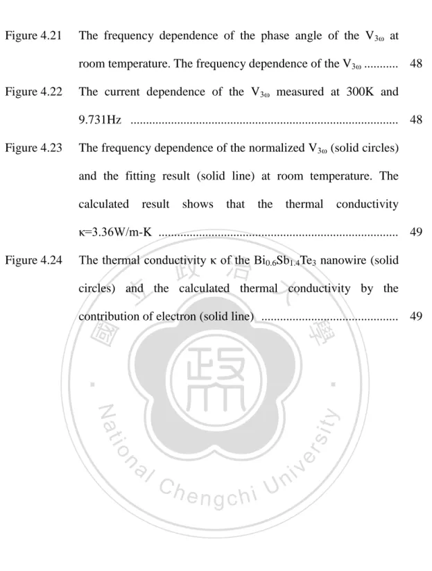
(12) Figure 4.21. The frequency dependence of the phase angle of the V3ω at room temperature. The frequency dependence of the V3ω ........... 48. Figure 4.22. The current dependence of the V3ω measured at 300K and 9.731Hz ...................................................................................... 48. Figure 4.23. The frequency dependence of the normalized V3ω (solid circles) and the fitting result (solid line) at room temperature. The calculated. result. shows. that. the. thermal. conductivity. κ=3.36W/m-K ............................................................................. 49. 政 治 大 the calculated thermal conductivity. The thermal conductivity κ of the Bi0.6Sb1.4Te3 nanowire (solid circles) and. 立. by the. contribution of electron (solid line) ............................................ 49. 學 ‧. ‧ 國 io. sit. y. Nat. n. al. er. Figure 4.24. Ch. engchi. xi. i n U. v.
(13) List of tables Chapter 3 Table 3.1. The weight percentage and atomic percentage of the Bi0.5Sb1.5Te3 ingot ................................................................................................. 12. Table 3.2. The weight percentage and atomic percentage of the Bi1.5Sb0.5Te3 ingot ................................................................................................. 13. Table 3.3. The weight percentage and atomic percentage of the Bi0.5Sb1.5Te3 film .................................................................................................. 15. Table 3.4. film. 16. Weight percentage and atomic percentage of three parts of the. 學. ‧ 國. Table 3.5. 政 治 大 .................................................................................................. 立. The weight percentage and atomic percentage of the Bi1.5Sb0.5Te3. nanowire No. 1 ................................................................................ 23 Weight percentage and atomic percentage of three parts of the nanowire No. 2 ................................................................................ 27. ‧. io. sit. y. Nat. n. al. er. Table 3.6. Ch. engchi. xii. i n U. v.
(14) Chapter 1 Introduction Thermoelectric materials can be used to convert thermal energy into electrical energy directly and vice versa. The performance of a thermoelectric material can be judge by the dimensionless parameter ZT=S2T/ρκ where S is the Seebeck coefficient, T is the used temperature, ρ is the resistivity and κ is the thermal conductivity. Bulk silicon (Si) has a high thermal conductivity (~150 W/m-K at room temperature), giving ZT≈0.01 at 300 K [1]. Recent report has shown that it is possible. 治 政 大 (EE) method [2]. To study which were synthesized by an aqueous electroless etching 立. to achieve ZT=0.6 at room temperature in rough Si nanowires of ~50 nm diameter. low-dimensional effects on thermoelectric properties is very interesting.. ‧ 國. 學. Many methods have been used to synthesize the bismuth telluride-based. ‧. nanowire. For example, chemical electrodeposition is applicable to fabricate. y. Nat. nanowires in prepatterned aluminum matrix (AAM) template [3]. In this research,. er. al. v i n thermoelectricCproperties on a same nanowire hengchi U n. Measuring. io. nanowires [4].. sit. single-crystalline BixSb2-xTe3 nanowires were synthesized by the on-film formation of. to obtain ZT is. challenging. In this research, we develop the technique to know the composition, crystalline orientation and thermoelectric properties on a same BixSb2-x Te3 nanowire.. 1.
(15) Chapter 2 Thermoelectric material Introduction This chapter gives an introduction of the thermoelectric effects and thermoelectric material. Section 2.1 gives a brief concept about thermoelectric effect. Section 2.2 discusses the figure of merit for thermoelectric materials.. 2.1 Thermoelectric effect The thermoelectric effect refers to phenomena by which either a temperature. 政 治 大 difference. These phenomena are known more specifically as the Seebeck effect, 立. difference creates an electric potential or an electric potential creates a temperature. Peltier effect, and Thomson effect.. ‧ 國. 學. Seebeck effect [5]. ‧. When two dissimilar conductors, A and B, constitute a circuit, a current will flow. sit. y. Nat. as long as the junctions of the two conductors are at different temperature. Conductor. io. al. n. colder junction.. er. A is defined as being positive to conductor B if the electrons flow from A to B at. Ch. engchi. Figure 2.1. i n U. v. The Seebeck effect. If the temperature difference ΔT between the two ends of a material is small, then the Seebeck coefficient which represent as S of a material is conventionally defined as S = −∆𝑉⁄∆𝑇 where ΔV is the thermoelectric voltage seen at the terminals.. 2.
(16) Peltier effect [5] When an electric current flows across a junction of two dissimilar conductors, heat is liberated or absorbed. When the electric current flows in the same direction as the Seebeck current, heat is absorbed at the hotter junction and liberated at the colder junction. The Peltier effect is defined as the reversible change in heat content when one coulomb crosses the junction. The direction in which the current flows determines whether heat is liberated or absorbed. This effect is reversible and is independent of the shape or dimension of the. 政 治 大 and the temperature of the junction, not of the contact. 立. materials composing the junction. It is a function of the compositions of the materials. ‧. ‧ 國. 學 sit. io. al. n. Figure 2.3. y. The Peltier effect. er. Nat. Figure 2.2. Ch. engchi. i n U. v. (a) The Seebeck circuit configured as a generator. (b) The Seebeck circuit configured as a cooler. 3.
(17) Thomson effect [5] The Thomson effect is define as the change in the heat content of a single conductor of unit cross section when a unit quantity of electricity flows along it through a temperature gradient of 1K. Consider a single conductor which has been heated at one point to some temperature T2. A thermal gradient will exist on either side of the heated point. Two points, P1 and P2, of equal temperature, T1<T2, will be found on either side of T2. If current flows in a circuit which include the single conductor, the temperature at P1 and. 政 治 大 to the direction of the temperature gradient. The electrons flowing past P will absorb 立 P2 will change. These changes are a result of the motion of the electrons with present 1. energy in moving against the temperature gradient and increase their potential energy.. ‧ 國. 學. The electrons following in the same direction as the thermal gradient will give up. ‧. energy and thus decrease their potential energy.. sit. y. Nat. Heat will accordingly be absorbed at P1, where the current direction is opposite. io. er. to the heat flow. Heat will be liberated at P2, where the current direction is the same as the heat flow. These changes in the heat content of the conductor are the Thomson. n. al. effect.. Ch. Figure 2.4. engchi. i n U. The Thomson effect. 4. v.
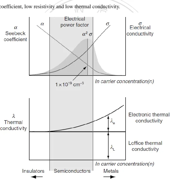
(18) 2.2 Figure of merit Because thermoelectric materials show the thermoelectric effect in a strong and/or convenient form, it can be demonstrate in power generation and refrigeration. A figure of merit for the thermoelectric device is defined as Z=S2/ρκ where S is the Seebeck coefficient, ρ is the resistivity, and κ is the thermal conductivity. The performance of a thermoelectric material can be judged by the dimensionless parameter ZT=S2T/ρκ where T is the use temperature. A greater ZT indicates a greater thermodynamic efficiency. A good thermoelectric material should have high Seebeck. 政 治 大. coefficient, low resistivity and low thermal conductivity.. 立. ‧. ‧ 國. 學. n. er. io. sit. y. Nat. al. Figure 2.5. Ch. engchi. i n U. v. Schematic dependence of electrical conductivity, Seebeck coefficient, power factor, and thermal conductivity on concentration of free carriers. [6] 5.
(19) The electrical conductivity is a reflection of the charge carrier concentration and all three parameters which occur in the figure-of-merit are functions of carrier concentration. The electrical conductivity increases with increase in carrier concentration while the Seebeck coefficient decreases, with the electrical power factor maximizing at a carrier concentration of around 1025/cm. The electronic contribution to the thermal conductivity λe, which in thermoelectric materials is generally around 1/3 of the total thermal conductivity, also increases with carrier concentration. Evidently the figure-of-merit optimizes at carrier concentrations which corresponds to semiconductor materials.. 立. 政 治 大. ‧. ‧ 國. 學. n. er. io. sit. y. Nat. al. Ch. engchi. 6. i n U. v.
(20) Chapter 3 Synthesis of nanowires Introduction This chapter presents how to synthesize nanowires and the analysis result of the nanowire. Stress-induced method was applied to synthesize nanowires. Section 3.1 introduces the acquired equipment and techniques. Section 3.2 shows how to make the target for the pulsed laser deposition system. Section 3.3 show how to deposit BixSb2-xTe3 thin film by pulsed laser deposition system. Section 3.4 shows the. 政 治 大. annealing process for growing nanowires. Section 3.5 shows the analysis result of the grown nanowires.. 立. ‧. ‧ 國. 學. n. er. io. sit. y. Nat. al. Figure 3.1. Ch. engchi. i n U. v. Schematic representation of the growth of BixSb2-xTe3 nanowires by stress-induce method. (a) Deposit BixSb2-xTe3 thin films on SiO2/Si substrates by using pulsed laser deposition system. (b) Seal the films in a vacuumed quartz tube. (c) Anneal the films at 350~500 ℃ for 5~21 days (d) Completion of BiSxb2-xTe3 nanowires growth. 7.
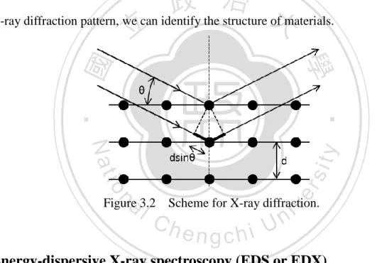
(21) 3.1 Experimental equipment and techniques X-ray diffraction (XRD) X-ray diffraction (XRD) is a common technique for analyzing the crystal structure of materials. Now consider a monochromatic X-ray beam with wavelength λ at an incident angle θ is incident in a crystalline material that the spacing between diffracting planes of the material is d. The path difference of the scattered X-ray by two nearby diffracting plane equals to 2d sin 𝜃 . The scattered X-ray interfere constructively when the path difference of the scattered X-ray equals to an integer. 政 治 大 X-ray diffraction pattern, we can identify the structure of materials. 立. multiple of the wavelength. This leads to Bragg law nλ = 2d sin 𝜃. By analyzing the. ‧. ‧ 國. 學. n. er. io. sit. y. Nat. al. Figure 3.2. i n U. v. Scheme for X-ray diffraction.. Ch. engchi. Energy-dispersive X-ray spectroscopy (EDS or EDX) Energy-dispersive X-ray spectroscopy (EDS or EDX) is an analytical technique used for the elemental analysis or chemical characterization of a sample. It relies on the investigation of an interaction of some source of X-ray excitation and a sample. Its characterization capabilities are due in large part to the fundamental principle that each element has a unique atomic structure allowing unique set of peaks on its X-ray spectrum To stimulate the emission of characteristic X-rays from a specimen, a high-energy beam of charged particles such as electrons or protons, or a beam of 8.
(22) X-rays, is focused into the sample being studied. The incident beam may excite an electron in an inner shell, ejecting it from the shell while creating an electron hole where the electron was. An electron from an outer, higher-energy shell then fills the hole, and the difference in energy between the higher-energy shell and the lower energy shell may be released in the form of an X-ray. As the energy of the X-rays are characteristic of the difference in energy between the two shells, and of the atomic structure of the element from which they were emitted, this allows the elemental composition of the specimen to be measured.. 政 治 大 Pulsed laser deposition (PLD) 立. Pulsed laser deposition is a technique for depositing thin film or making. ‧ 國. 學. nanoparticle. To deposit thin film, a high power pulsed laser is focused in a vacuum. ‧. chamber and hit the target. The material which is to be deposited then be vaporized. sit. y. Nat. from the target and form a thin film on the substrate. Substituting substrate into liquid. io. then it can get nanoparticle instead of thin film.. n. al. Ch. engchi. er. nitrogen-cooled copper plate and following a similar procedure in background gas. i n U. v. Figure 3.3 Pulsed laser deposition system for nanoparticles and thin film fabrication.. 9.
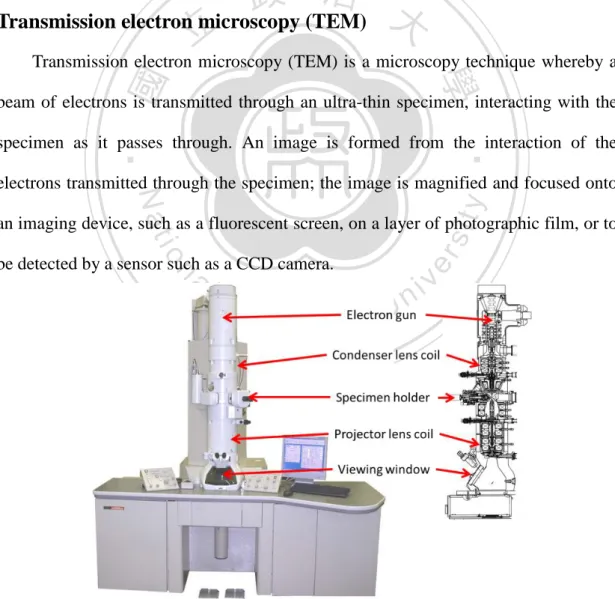
(23) Scanning electron microscope (SEM) A scanning electron microscope (SEM) is a type of electron microscope that images a sample by scanning it with a beam of electrons. Electron beam is emitted from an electron gun and be focused by condenser lenses to a spot and interacts with the sample. The energy exchange between the electron beam and the sample results in emission of secondary electrons by inelastic scattering and the emission of electromagnetic radiation, the reflection of high-energy electrons by elastic scattering, each of which can be detected by specialized detectors. The signal then is converted. 政 治 大 Transmission electron microscopy (TEM) 立. into image and display on the monitor.. Transmission electron microscopy (TEM) is a microscopy technique whereby a. ‧ 國. 學. beam of electrons is transmitted through an ultra-thin specimen, interacting with the. ‧. specimen as it passes through. An image is formed from the interaction of the. sit. y. Nat. electrons transmitted through the specimen; the image is magnified and focused onto. io. be detected by a sensor such as a CCD camera.. n. al. Figure 3.4. Ch. engchi. er. an imaging device, such as a fluorescent screen, on a layer of photographic film, or to. i n U. v. Exterior view of TEM and cross section of column.. 10.
(24) Selected area diffraction (SAD) In a TEM, a thin crystalline specimen is subjected to a parallel beam of high-energy electrons. Because the wavelength of high-energy electrons is a few thousandths of a nanometer and the spacing between atoms in a solid is about a hundred times larger, the atoms act as a diffraction grating to the electrons, which are diffracted. That is, some fraction of them will be scattered to particular angles, determined by the crystal structure of the sample, while others continue to pass through the sample without deflection. As a result, the image on the screen of the. 政 治 大 corresponding to a satisfied diffraction condition of the sample's crystal structure. 立. TEM will be a series of spots—the selected area diffraction pattern, SADP, each spot. ‧ 國. 學. 3.2 Target preparation. ‧. To prepare the target of the pulsed laser deposition system, Bi2Te3 and Sb2Te3. sit. y. Nat. powders were mixed by a particular ratio. The mixed powder is sealed into a. io. er. vacuumed quartz tube The tube with the powder inside was put into the furnace and heated up to 750℃. The melting point of Bi2Te3 and Sb2Te3 are 585℃ and 580℃. al. n. v i n respectively Temperature was kept C hat 750℃ for a fewUhours to make sure the Bi Te engchi 2. 3. and Sb2Te3 were form into BixSb2-xTe3 compound. The tube containing the melting compound was slowly cool down to room temperature and formed a bulk. The bulk was cut into ingot. The structure and the composition of the ingot were checked by the XRD and EDX respectively.. 11.
(25) 立. Figure 3.5. 政 治 大. X-Ray diffraction pattern of Bi0.5Sb1.5Te3 ingot.. ‧. ‧ 國. 學. n. er. io. sit. y. Nat. al. Figure 3.6. Ch. engchi. i n U. v. EDX spectrum of Bi0.5Sb1.5Te3 ingot.. Table 3.1 The weight percentage and atomic percentage of the Bi0.5Sb1.5Te3 ingot. Element. Weight%. Atomic%. Bi. 14.48. 9.24. Sb. 28.4. 31.09. Te. 57.13. 59.68. 12.
(26) 立. Figure 3.7. 政 治 大. X-Ray diffraction pattern of Bi1.5Sb0.5Te3 ingot.. ‧. ‧ 國. 學. n. er. io. sit. y. Nat. al. Figure 3.8. Ch. engchi. i n U. v. EDX spectrum of Bi1.5Sb0.5Te3 ingot.. Table 3.2 The weight percentage and atomic percentage of the Bi1.5Sb0.5Te3 ingot. Element. Weight%. Atomic%. Bi. 40.83. 29.51. Sb. 8.04. 9.97. Te. 51.23. 60.52. 13.
(27) 3.3 Film deposition Cut the silicon (Si) wafer with 300nm silicon oxide (SiO2) into 9~600mm2 rectangular SiO2/Si substrates. Substrates were cleaned by using acetone, isopropyl alcohol and deionized water in ultrasonic bath for 10 minute each, respectively. Stick the SiO2/Si substrates on the substrate holder and fix the target on the target holder of the pulsed laser deposition system (PLD). The distance between the target and the substrate was 8 cm. Adjust the laser to focus on the surface of the target. Vacuum the chamber by rotary pump and cryopump to the pressure lower than. 政 治 大 for a period of time at room temperature. The total thickness of the formed 立 5.0×10⁻⁷ torr. Use different power and different frequency of the laser to hit the target. BixSb2-xTe3 films were ranged from few tens of nanometer to few hundreds of. ‧ 國. 學. nanometers. The composition of the film is confirm by the EDX. ‧. n. er. io. sit. y. Nat. al. Figure 3.9. Ch. engchi. i n U. v. SEM image of Bi0.5Sb11.5Te3 thin film that deposited for 1 hour. The power and the frequency of the laser are 170mJ and 10Hz respectively. The rectangular shows the corresponding area of EDX analysis.. 14.
(28) Figure 3.10. EDX spectrum of Bi0.5Sb1.5Te3 film.. 政 治 大 Weight%. Table 3.3 The weight percentage and atomic percentage of the Bi0.5Sb1.5Te3 film.. 立. Element. Te. 9.59. 學. Sb. 15.00. ‧ 國. Bi. Atomic%. 27.86 57.14. 30.57 59.83. ‧. n. er. io. sit. y. Nat. al. Ch. engchi. i n U. v. Figure 3.11 AFM analysis shows that the thickness of the film is about 38nm.. 15.
(29) Figure 3.12. 立. 政 治 大 Sb Te thin film that deposited for 5 min. The. SEM image of Bi1.5. 0.5. 3. ‧ 國. 學. power and the frequency of the laser are 160mJ and 30Hz respectively. The rectangular shows the corresponding area of EDX analysis.. ‧. n. er. io. sit. y. Nat. al. Figure 3.13. Ch. engchi. i n U. v. EDX spectrum of Bi1.5Sb0.5Te3 film.. Table 3.4 The weight percentage and atomic percentage of the Bi1.5Sb0.5Te3 film. Element. Weight%. Atomic%. Bi. 42.43. 30.90. Sb. 7.44. 9.30. Te. 50.13. 59.80. 16.
(30) 立. 政 治 大. Figure 3.14 AFM analysis shows that the thickness of the film is about 88nm.. ‧ 國. 學 ‧. 3.4 Annealing process. y. Nat. The films were sealed in a vacuumed quartz tube below the pressure of 5×10⁻⁶. er. io. sit. mbar and anneal them at 350~500 ℃ for 5~21 days. The thermal expansion coefficient of the BixSb2-xTe3 film (~13.4×10⁻⁶/℃), SiO2 (0.5×10⁻⁶/℃) and Si. al. v i n /℃) are different. During the substrate restricted the C hthe annealing process, engchi U n. -6. (2.4×10. expansion of the film and put the film under compressive stress. The nanowires then. grew from the film in order to release the compressive stress. The films were cooled down in air. Scanning electron microscope (SEM) and optical microscope (OM) were used to observe the nanowire.. 17.
(31) 立. OM image of the Bi0.5Sb1.5Te3 thin film after annealing at 350 ℃for 21. 學. ‧ 國. Figure 3.15. 政 治 大. days.. ‧. n. er. io. sit. y. Nat. al. Figure 3.16. Ch. engchi. i n U. v. Side view SEM image of Bi0.5Sb1.5Te3 film after annealing at 350 ℃ for 21 days. 18.
(32) 立. OM image of the Bi1.5Sb10.5Te3 thin film after annealing at 490 ℃for 5. 學. ‧ 國. Figure 3.17. 政 治 大. days.. ‧. n. er. io. sit. y. Nat. al. Figure 3.18. Ch. engchi. i n U. v. Side view SEM image of Bi1.5Sb10.5Te3 film after annealing at 490 ℃ for 5 days. 19.
(33) 3.5 Analysis results In order to analyze a single nanowire by transmission electron microscopy (TEM), the wire was suspended on a measurement platform so that electron beam can penetrate the wire. The wire is divided into three parts. The end close to the heater is defined as top part. The end away from the heater is defined as bottom part. Between the top and the bottom is the middle part. To see if the wire is well crystalized or not and the growth orientation of the nanowire, selected area diffraction (SAD) was taken. To see the distribution of the bismuth, antimony and telluride in the wire, EDX. 政 治 大. line-scan profile was taken. To know the ratio between the three element EDX point scan has been done.. 立. ‧. ‧ 國. 學. Nanowire No.1. n. er. io. sit. y. Nat. al. Figure 3.19. Ch. engchi. i n U. v. SEM image of a suspend nanowire No.1 which grown from Bi0.5Sb1.5Te3 film after annealing at 500 ℃for 5 days. The nanowire is 150 nm in diameter. The electrodes had already deposited by the FIB. 20.
(34) 立. Figure 3.20. 政 治 大 TEM image of the nanowire No. 1.. ‧. ‧ 國. 學. n. er. io. sit. y. Nat. al. Figure 3.21. Ch. engchi. i n U. v. Selected area diffraction pattern of the nanowire No. 1.. 21.
(35) (a). (b). 立. 政 治 大. ‧. ‧ 國. 學 sit. n. al. er. io. Figure 3.22. y. Nat. (c). Ch. engchi. i n U. v. The scanning TEM image of (a) top (b) middle (c) bottom part of the nanowire No.1. The EDX line-scan profile show that Bismuth, antimony and telluride homogeneously distributed through the nanowire. 22.
(36) (a). (b). 政 治 大. 立. ‧. ‧ 國. 學. (c). n. er. io. sit. y. Nat. al. Ch. engchi. i n U. v. Figure 3.23 EDX point-scan spectrum of the (a) top (b) middle (c) bottom part of the nanowire No.1. The inset shows the corresponding point. Table 3.5 Weight percentage and atomic percentage of three parts of the nanowire Element. Atomic%. Atom number. Top. Middle. Bottom. Top. Middle. Bottom. Bi. 13.13. 13.20. 12.87. 0.62. 0.62. 0.62. Sb. 29.53. 28.88. 28.79. 1.38. 1.38. 1.38. Te. 57.52. 57.92. 58.34. 2.71. 2.71. 2.80. 23.
(37) Nanowire No.2. 立. ‧ 國. 學. SEM image of a suspend nanowire No.2 which grown from. ‧. Bi1.5Sb0.5Te3 film after annealing at 490 ℃for 5 days. The nanowire. io. sit. y. Nat. is 220 nm in diameter.. n. al. er. Figure 3.24. 政 治 大. Ch. engchi. i n U. v. Figure 3.25 TEM image of the nanowire No. 2. 24.
(38) 立. 政 治 大. ‧ 國. 學 ‧. Figure 3.26 TEM image of the nanowire No. 2.. n. er. io. sit. y. Nat. al. Figure 3.27. Ch. engchi. i n U. v. Selected area diffraction pattern of the nanowire No. 2. 25.
(39) (a). (b). 立. 政 治 大. ‧. ‧ 國. 學. n. al. er. io. sit. y. Nat. (c). Ch. engchi. i n U. v. Figure 3.28 The scanning TEM image of (a) top (b) middle (c) bottom part of the nanowire No.2. The EDX line-scan profile show that Bismuth, antimony and telluride homogeneously distributed through the nanowire.. 26.
(40) (a). (b). 政 治 大. 立. ‧. ‧ 國. 學. (c). n. er. io. sit. y. Nat. al. Ch. engchi. i n U. v. Figure 3.29 EDX point-scan spectrum of the (a) top (b) middle (c) bottom part of the nanowire No.2. The inset shows the corresponding point. Table 3.6 Weight percentage and atomic percentage of three parts of the nanowire Element. Atomic%. Atom number. Top. Middle. Bottom. Top. Middle. Bottom. Bi. 37.54. 37.34. 37.46. 1.66. 1.66. 1.66. Sb. 7.64. 7.74. 7.57. 0.34. 0.34. 0.34. Te. 54.83. 54.92. 54.97. 2.43. 2.44. 2.44. 27.
(41) Chapter 4 Thermoelectric property measurements of nanowires. Introduction This chapter shows that how to measure the thermoelectric properties and the measurement result. In order to applied 3ω method to measure the thermal conductivity, nanowire was suspended on the measurement platform to allow the temperature fluctuation. In order to measure the thermoelectric properties, electrodes, heater and thermometers were fabricated on the measurement platform. Secstion4.1. 政 治 大 the measurement platform and suspend a wire on it. Section 4.4 shows how to 立. introduces the acquired equipment and techniques. Section 4.2 shows how to fabricate. measure the thermoelectric properties of the nanowire. Section 4.5 shows the. sit. y. Nat. 4.1 Experimental equipment and techniques. ‧. ‧ 國. 學. measurement result.. io. er. Photolithography. Photolithography is a process used in microfabrication to selectively remove. al. n. v i n parts of a thin film or the bulk C of a substrate. It uses U h e n g c h i light to transfer a pattern from a mask to a light-sensitive chemical photoresist on the substrate. A series of chemical. treatments then either engraves the exposure pattern into, or enables deposition of a new material in the desired pattern upon, the material underneath the photo resist.. Dry etch Dry etching refers to the removal of material, typically a masked pattern of semiconductor material, by exposing the material to a bombardment of ions that dislodge portions of the material from the exposed surface. Unlike with many of the wet chemical etchants used in wet etching, the dry etching process typically etches directionally or anisotropically. 28.
(42) Wet etch The wafer is immersed in a bath of etchant, which must be agitated to achieve good process control. Etching a (100) silicon surface through a rectangular hole in a masking material creates a pit with flat sloping <111>-oriented sidewalls and a flat <100>-oriented bottom. The <111>-oriented sidewalls have an angle to the surface of the wafer of: tan−1 √2 = 54.7°. If the original rectangle was a perfect square, the pit when etched to completion displays a pyramidal shape.. Lift-off process [7]. 政 治 大 Metallic thin film is then deposited onto the patterned resist layer. A wet chemical 立. A polymer resist layer is patterned first by optical or e-beam lithography.. solution dissolves the resist layer, which also lifts off the metallic thin film on top of. ‧ 國. 學. resist layer from the substrate. Only the metallic film deposited through the resist. sit. y. Nat. onto the substrate as a metallic pattern of reverse polarity.. ‧. pattern opening onto the substrate remains. In this way, the resist pattern is transferred. io. er. Focused ion beam (FIB). FIB systems operate in a similar fashion to a scanning electron microscope (SEM). al. n. v i n C h and as the name except, rather than a beam of electrons implies, FIB systems use a engchi U. finely focused beam of ions (usually gallium) that can be operated at low beam currents for imaging or high beam currents for site specific sputtering or milling. An FIB can used to deposit material via ion beam induced deposition. FIB-assisted chemical vapor deposition occurs when a gas, such as tungsten hexacarbonyl (W(CO)6) is introduced to the vacuum chamber and allowed to chemisorb onto the sample. By scanning an area with the beam, the precursor gas will be decomposed into volatile and non-volatile components; the non-volatile component, such as tungsten, remains on the surface as a deposition.. 29.
(43) Probe station with micropositioner A probe station can be used to physically acquire signals from the internal nodes of a semiconductor device. The probe station utilizes manipulators which allow the precise positioning of thin needles on the surface of a semiconductor device. Here, the setup is used for manipulating nanowires. The micropositioner is equip with cat-whisker probe tip and fixed on probe station.. 政 治 大. 立. ‧. ‧ 國. 學. Figure 4.1 Set up of probe station with micropositioner for manipulating nanowire.. y. Nat. io. sit. Four-point probe method. n. al. er. Current is supplied via a pair of current leads generate a voltage drop across the. i n U. v. specimen and also across the current leads themselves. To avoid including that in the. Ch. engchi. measurement, a pair of voltage leads is connected to the specimen. The accuracy of the technique comes from the fact that almost no current flows in the sense wires, so the voltage drop V=RI is extremely low.. Figure 4.2 Four-probe configuration for measuring the resistivity of a wire.. 30.
(44) Resistance thermometer Resistance thermometer is sensor used to measure temperature by correlating the resistance of the resistance thermometer element with temperature. The temperature dependence of electrical resistance of conductors is to a great degree linear and can be described by the approximation below: ρ(T) = 𝜌0 [𝛼0 (𝑇 − 𝑇0 )]. 𝛼0 =. 1 𝛿𝜌 [ ] 𝜌0 𝛿𝑇 𝑇=𝑇. 0. ρ0 just corresponds to the specific resistance temperature coefficient at a specified reference value. That of a semiconductor is however exponential:. 治 政 ρ(T) = 𝑆𝛼 大 𝐵 𝑇. 立. where S is defined as the cross sectional area and α and B are coefficients determining. ‧ 國. 學. the shape of the function and the value of resistivity at a given temperature.. ‧. 3ω method for thermal conductivity measurement [8]. y. Nat. io. sit. In this method, either the specimen itself serves as a heater and at the same time. n. al. er. a temperature sensor, if it is electrically conductive and with a temperature-dependent. i n U. v. electric resistance. Feeding an ac electric current of the form 𝐼0 sin 𝜔𝑡 into the. Ch. engchi. specimen creates a temperature fluctuation on it at the frequency 2ω, and accordingly a resistance fluctuation at 2ω. This further leads to a voltage fluctuation at 3ω across the specimen. Consider a uniform rod- or filament-like specimen in a four-probe configuration as for electrical resistance measurement. The two outside probes are used for feeding an electric current, and the two inside ones for measuring the voltage across the specimen. The specimen in between the two voltage probes is suspended to allow the temperature fluctuation. All the probes have to be highly thermal conductive, to heat sink the specimen at these points to the substrate. The specimen has to be maintained 31.
(45) in a high vacuum and the whole setup is heat shielded to the substrate temperature to minimize the radial heat loss through gas convection and radiation.. Figure 4.3. Illustration of the four-probe configuration for measuring the specific. 政 治 大 In such a configuration 立and with an ac electrical current of the form 𝐼 sin 𝜔𝑡 heat and thermal conductivity of a wire.. 0. ‧ 國. 學. passing through the specimen, the heat generation and diffusion along the specimen can be described by the following partial differential equation and the initial and. ‧. boundary conditions:. (4.1). 𝑇(0, 𝑡) = 𝑇0 { 𝑇(𝐿, 𝑡) = 𝑇0 𝑇(𝑥, −∞) = 𝑇0. (4.2). n. al. er. io. sit. y. Nat. 𝜕 𝜕2 𝐼02 sin 𝜔𝑡 [𝑅 + 𝑅 ′ (𝑇(𝑥, 𝑡) − 𝑇0 )] ρ𝐶𝑝 𝑇(𝑥, 𝑡) − 𝜅 2 𝑇(𝑥, 𝑡) = 𝜕𝑡 𝜕𝑥 𝐿𝑆. Ch. engchi U. v ni. where Cp, κ, R, and ρ are the specific heat, thermal conductivity, electric resistance and mass density of the specimen at the substrate temperature T0, respectively. 𝑅 ′ = (𝑑𝑅/𝑑𝑇) 𝑇0 . L is the length of the specimen between voltage contacts, and S the cross section of the specimen. Let ∆(𝑥, 𝑡) denote the temperature variation from T0. i.e. ∆(𝑥, 𝑡) = 𝑇(𝑥, 𝑡) − 𝑇0, Equation (3-1-1) and (3-1-2) become 𝜕2 𝜕 ∆(𝑥, 𝑡) − 𝛼 2 ∆(𝑥, 𝑡) − 𝑐 sin2 𝜔𝑡 ∙ ∆(𝑥, 𝑡) = 𝑏 sin2 𝜔𝑡 𝜕𝑥 𝜕𝑡. (4.3). where 𝛼 = 𝜅/𝜌𝐶𝑝 is the thermal diffusivity and b = 𝐼02 𝑅/𝜌𝐶𝑝 𝐿𝑆, c = 𝐼02 𝑅 ′ /𝜌𝐶𝑝 𝐿𝑆 The temperature distribution along the specimen would be:. 32.
(46) ∞. T(x, t) − 𝑇0 = ∆0 ∑ 𝑛=1. [1 − 1(−1)]𝑛 sin(2𝜔𝑡 + 𝜙𝑛 ) 𝑛𝜋𝑥 [1 − ] × sin 3 2𝑛 𝐿 √1 + cot 2 𝜙𝑛. (4.4). where cot 𝜙𝑛 = 2𝜔𝛾/𝑛2 and ∆0 = 2𝛾𝑏⁄𝜋 = 2𝐼02 𝑅⁄(𝜋𝜅𝑆/𝐿) is the maximum dc temperature accumulation at the center of the specimen. γ ≡ 𝐿2 ⁄𝜋 2 𝛼 is the characteristic thermal time constant of the specimen for the axial thermal process. ∆0 is only κ dependent. The information of Cp is included in the fluctuation amplitude of the temperature around the dc accumulation. By solving the partial difference equation, the resistance fluctuation can be expressed. 政 治 大 sin(2𝜔𝑡 + 𝜙 ). as ∞. ′. [1 − 1(−1)𝑛 ]2 𝑛 [1 − ] 4 2𝜙 2𝜋𝑛 √1 + cot 𝑛 𝑛=1. 立. δR = 𝑅 ∆0 ∑. (4.5). ‧ 國. 學. As a product of the total resistance R + δR and the current 𝐼0 sin 𝜔𝑡, the. ‧. voltage across the specimen contains a 3ω component V3ω(t). Only taking the n=1. io. y. 𝜋 4 𝜅𝑆√1 + (2𝜔𝛾)2. al. sit. 2𝐼03 𝐿𝑅𝑅 ′. sin(3𝜔𝑡 − 𝜙). (4.6). er. 𝑉3𝜔 (𝑡) ≈ −. Nat. term at low frequencies, the 3ω component can be express as. v. n. The root-mean-square (rms) values of voltage across the specimen contains a 3ω component 3. 𝑉3𝜔 ≈. 4𝐼 𝐿𝑅𝑅. ′. Ch. engchi. i n U. (4.7). 𝜋 4 𝜅𝑆√1 + (2𝜔𝛾)2. By fitting the experimental data to this formula, we can get the thermal conductivity κ and thermal time constant γ of the specimen. The specific heat can then be calculated as 𝐶𝑝 = 𝜋 2 𝛾𝜅⁄𝜌𝐿2. (4.8). 33.
(47) 4.2 Primary measurement platform fabrication First, silicon (Si) wafer with Si3N4 on the both sides was covered with photoresist by spin coating. Then photoresist was exposed to a rectangular pattern of ultraviolet light. After exposure, soluble photoresist would be developed by the developer. The wafer was then put into the RIE system. The Si3N4 without the protection of the photoresist would be etched by the reactive-ion. Next, the wafer is immersed in a bath of sodium hydroxide solution (NaOH). Si that expose to NaOH would be etch and then create cavities. Wafer with Si3N4 membranes would be complete after stripping.. 立. 政 治 大. ‧. ‧ 國. 學. n. er. io. sit. y. Nat. al. Ch. engchi. i n U. v. Figure 4.4 Schematic representation of making Si3N4 membrane: (Step 1) Substrate spin coat with photoresist. (Step 2) Photoresist be exposed to a pattern of ultraviolet light. (Step 3) Soluble photoresist be developed by the developer. (Step 4) Remove Si3N4 by dry etch. (Step 5) Create cavities and leave a Si3N4 membrane by wet etch. (Step 6) Strip the photoresist. 34.
(48) Lift-off process was used to make the contact pads of the measurement platform. Si wafer with Si3N4 membrane was cover with photoresist by spin coating. Then photoresist was exposed to a pattern of contact pads of ultraviolet light. After exposure, soluble photoresist would be developed by the developer. Use the evaporator to deposit Ni/Au and then lift-off the photoresist by acetone. The primary measurement platform would be ready to be used after lift-off.. 立. 政 治 大. ‧. ‧ 國. 學. n. er. io. sit. y. Nat. al. Ch. engchi. i n U. v. Figure 4.5 Schematic representation of depositing the contact pads: (Step 1) Substrate spin coat with photoresist. (Step 2) Photoresist be exposed to a pattern of ultraviolet light. (Step 3) Soluble photoresist be developed by the developer. (Step 4) Deposit Ni/Au. (Step 5) Lift-off the photoresist.. 35.
(49) 4.2 Nanowires suspension and completion of measurement platform Several methods were used to suspend the nanowire and complete the measurement platform.. Method one First, the primary measurement platform was immersed in the DI water and put into the ultrasonic cleaner. Then the Si3N4 membrane was broken by the ultrasonic wave to open a window in the primary measurement platform. Next, the nanowire was picked up by a cat–whisker probe tip which manipulated by a micropositioner. 政 治 大 primary measurement platform and deposit the six electrodes by the FIB. 立. under the optical microscope. Then the nanowire was suspended on the on the. ‧. ‧ 國. 學. n. er. io. sit. y. Nat. al. Ch. engchi. i n U. v. Figure 4.6 Schematic representation of suspend the nanowire and deposit the electrodes by method one. (1)Prepare a primary measurement platform with membrane. (2)Break the membrane by ultrasonic wave. (3)Suspend the wire. (4)Deposit electrode by FIB. 36.
(50) 政 治 大. Figure 4.7 SEM image of a suspended nanowire.. 立. Method two. ‧ 國. 學. Put the nanowire on the primary measurement platform. Part of the nanowire was laid on the Si3N4 membrane. The resistance thermometers, current leads and voltage. ‧. leads would be made by the electron-beam lithography. Two kind of pattern were used. y. Nat. n. al. er. io. sit. in the measurement. Next, the membrane was etched by the ICP or broke by the tip.. Ch. engchi. 37. i n U. v.
(51) 立. 政 治 大. Figure 4.8 Schematic representation of suspend the nanowire and deposit the. ‧ 國. 學. electrodes by method two. (a) and (b) follow the same procedure but. ‧. with different pattern. (1)Prepare a primary measurement platform with. sit. y. Nat. membrane. (2)Put the wire on the primary measurement platform.. io. er. (3)Make the thermometer and electrodes by lift-off process. (4)Remove the membrane.. n. al. Ch. engchi. i n U. v. Figure 4.9 SEM top view image of the suspended nanowire. 38.
(52) 立. 政 治 大. ‧ 國. 學 sit. y. Nat. Method three. ‧. Figure 4.10 SEM tilt view image of the suspended nanowire.. io. er. First, the resistance thermometers, current leads were made by the electron-beam lithography on the primary measurement platform. The Si3N4 membrane can break by. al. n. v i n C plasma the ultrasonic wave, reacting ion, tip to open a window. Next, the U h e norgtungsten i h c nanowire was hanged across two resistance thermometers with two ends of the wire. attach to the current lead. As two electrodes of the thermometer was also the voltage lead of 4-point probes method, the contacts of the nanowire and thermometer would be covered with a layer of platinum which are deposited by the FIB to make a better contact and also the contact of current leads.. 39.
(53) 立. 政 治 大. Figure 4.11 Schematic representation of suspend the nanowire and deposit the. ‧ 國. 學. electrodes by method three. (1)Make the thermometers on the primary. ‧. measurement platform by the lift-off process. (2)Break the membrane by. sit. y. Nat. ultrasonic wave. (3)Suspend the wire. (4)Deposit a layer of platinum to. io. n. al. er. cover the contact.. Ch. engchi. i n U. v. Figure 4.12 SEM image of the suspended nanowire. 40.
(54) 4.4 Thermoelectric properties measurement of the nanowire 4.4.1 Resistivity measurement Four-point probe method was applies to measure the resistivity. Feed an AC current via a pair of current leads into the specimen and measure the root mean square of the voltage difference via a pair of voltage leads. According to V = IR and ρ = RA/ℓ where V, I, R, ρ, A and ℓ are voltage difference, current, resistance, resistivity, cross-section area of the wire and length between a pair of voltage leads respectively, one can get the resistivity of the nanowire.. 政 治 大 4.4.2 Seebeck measurement 立. To get the Seebeck coefficient, temperature gradient is generated by heater. ‧ 國. 學. across the sample and thermoelectric voltage that is generated by the Seebeck effect is. ‧. measure. To generate the temperature gradient, the heater is placed at one end of the. sit. y. Nat. sample and an AC current with frequency 1ω with magnitude equals to I sin 𝜔𝑡 is. io. er. applied to the heater. Heater would produce heat because of the Joule heating. Because heat that produced by the heater is proportional to the square of the current. al. n. v i 2 n C h of the wire Q ∝U(𝐼 sin2 𝜔𝑡)𝑅 multiplied by the electrical resistance engchi. where Q is the. heat that produced by the heater and R is the electrical resistance of the sample and sin2 𝛼 = (1 − cos 2𝛼 ⁄2), so the heater would be heated at frequency 2ω. As the heater is heated at frequency 2ω, the temperature fluctuation on the sample would be also at frequency 2ω. As a length of metallic wire or part of the sample is used as the sensor of the thermometer, temperature coefficient of electrical resistance of them are needed to be known at first. As temperature is fluctuated at frequency 2ω, resistance of the sensor would change at frequency 2ω. By apply a DC current to the sensor and measure the change of the voltage difference between the two end of the sensor at frequency 2ω by using lock-in amplifier, it would able to know the resistance change 41.
(55) of the sensor. Already knowing the temperature coefficient of electrical resistance of the sensor, how much degree different been created between two end of the sample would be known. By knowing the temperature difference and also measuring the thermoelectric voltage of two end of the sample, Seebeck coefficient can be calculated by the formula: S = − △ V⁄△ 𝑇.. 4.4.3 Thermal conductivity measurement 3ω method was applied for the thermal conductivity measurement. The. 政 治 大 between the two voltage probes should be suspended to allow the temperature 立 measurement setup is much like the setup of resistivity measurement. The specimen. ‧ 國. 學. fluctuation. Feed an AC current of the form 𝐼0 sin 𝜔𝑡 via a pair of current leads into the specimen and lock the V3ω signal via a pair of voltage leads. Theoretical. ‧. calculation 𝑉3𝜔 ≈ 4𝐼 3 𝐿𝑅𝑅 ′⁄𝜋 4 𝜅𝑆√1 + (2𝜔𝛾)2. By fitting the experimental data to. sit. y. Nat. this formula, one can get the thermal conductivity κ and thermal time constant γ of the. io. er. specimen. Further detail will shoe in the. There are two ways to perform the measurement. In the first, the measurement. al. n. v i n platform is maintained at fixedC temperatures, and then h e n g c h i U the frequency dependence of V3ω is measured. In this way, we can check the I3 and the 1⁄√1 + (2𝜔𝛾)2. dependencies of V3ω as well as the relation tan 𝜙 = 2𝜔𝛾. In the second way of measurement, the temperature of the measurement platform is slowly increase or decrease, and the working frequency of the lock-in amplifier is changed between a few set values. The maximum working frequency is adjusted by keeping 2ωγ<4.. 42.
(56) 4.4.4 Pattern design Several inner electrode pattern designs are use in the measurement.. Pattern one For resistivity and thermal conductivity measure, electrodes A and B are current leads. Electrodes C and D are connected to a locking amplifier. For Seebeck measurement, part of the nanowire between the contact of electrode C and E is the high temperature sensor and part of the wire between the contact of electrode D and F is the low temperature sensor. Current via electrode A and B feed into the sensors.. 政 治 大. Electrodes C and D is a pair of voltage lead for measuring the voltage difference that is generate by the Seebeck effect.. 立. ‧. ‧ 國. 學 er. io. sit. y. Nat. al. n. v i n C h representationUof pattern one Figure 4.13 Schematic engchi. Pattern two. For resistivity and thermal conductivity measure, electrodes A and B are current leads. Electrodes C and D are connected to a locking amplifier to lock the V1ω and V3ω signal. For Seebeck measurement, a length of gold wire vertical to the heater between the contact of electrode G and H is the high temperature sensor of the thermometer Th and a length of gold wire between the contact of electrode I and J is the low temperature sensor of the thermometer Tc. Current via electrode E and F feed into the thermometer Th and Tc. Electrodes C and D is a pair of voltage lead for measuring the voltage difference that is generate by the Seebeck effect. 43.
(57) Figure 4.14 Schematic representation of pattern two. Pattern three. 政 治 大 leads. Electrodes C and D are connected to a locking amplifier to lock the V 立. For resistivity and thermal conductivity measure, electrodes A and B are current 1ω. and. V3ω signal. For Seebeck measurement, current via electrode C and E feed into the. ‧ 國. 學. thermometer Th and via electrode D and F feed into the thermometer Th. A length of. ‧. gold wire parallel to the heater between the contact of electrode H and G is the high. sit. y. Nat. temperature sensor of the thermometer Th and a length of gold wire between the. io. er. contact of electrode I and J is the low temperature sensor of the thermometer Tc. Electrodes C and D is a pair of voltage lead for measuring the voltage difference that. n. al. Ch. is generate by the Seebeck effect... engchi. i n U. v. Figure 4.15 Schematic representation of pattern three. 44.
(58) 4.5 Measurement results Resistivity measurement The measurement of resistivity by the four-probe point method of the Bi0.62Sb1.38Te2.74 nanowire with diameter 150nm was excited by a constant alternating current about 0.1μA, where it is a sine wave 𝐼0 sin 𝜔𝑡 profile with constant frequency f=9.731Hz. The experimental data of resistivity in temperature range 3.5 – 300 K of the nanowire was shown in Figure 4.16. The corresponding voltage signal with less than two degree shift was picked up by the lock-in amplifier (Figure4.17).. 立. 15. 政 治 大. ‧ 國. 學. 10. ‧. 5. y. Nat. io. 0. 50. 100. al. 150. 200. T (K). 250. 300. er. 0. sit. Resistivity (-m). 20. n. v i n Ctheh Bi Sb Te nanowire Figure 4.16 The resistivity of with diameter 150nm. engchi U 0.6. 1.4. 3. 5. Phase (deg.). 4 3 2 1 0. 0. 50. 100. 150. 200. 250. 300. T (K). Figure 4.17 The temperature dependence of the phase angle of V. 45.
(59) Seebeck measurement Figure 4.18 shows thermoelectric voltage ΔV is linear dependence to the temperature difference ΔT at 200K. Figure 4.19 shows the obtained Seebeck coefficient from 130K to 230K.. 20. V (V). 15. T=200K 10. 5. 政 治 大. 0 -0.5. -0.4. -0.3. -0.2. -0.1. T (K). 學. ‧ 國. 立. 0.0. ‧. Figure 4.18 The temperature difference ΔT dependence of the thermoelectric voltage. y. Nat. Seebeck coeff. (V/K). n. al. er. io 100. sit. ΔV at T=200K. Ch. engchi. i n U. v. 50. 0 100. 200. 300. T (K) Figure 4.19 The Seebeck coefficient of the Bi0.6Sb1.4Te3 nanowire with diameter 150nm. 46.
(60) Thermal conductivity measurement We applied the 3ω method to measure the thermal conductivity of a suspended Bi0.6Sb1.4Te3 nanowire with diameter 150nm by using the approximation solution: 𝑉3𝜔 ≈ 4𝐼 3 𝐿𝑅𝑅 ′ ⁄𝜋 4 𝜅𝑆√1 + (2𝜔𝛾)2 . The calculated R′ = (𝑑𝑅 ⁄𝑑𝑇) 𝑇0 is shown in Figure 4.20.. 15 12. 立. 6. 政 治 大. 學. 3. 0 100 120 140 160 180 200 220 240 260 280. T (K). Nat. sit. y. ‧. ‧ 國. R'. 9. io. er. Figure 4.20 The temperature dependence of R'. al. n. v i n There is a test for choosingCappropriate exciting U h e n g c h i current. The working frequency. should adjusted by keeping tan ϕ < 4 and experimental data of tan ϕ should not curve away from linearity. The frequency dependence of the phase angle of the V3ω with different exciting currents at room temperature is shown in Figure 4.21. It shows that applying 1.0μA, tan ϕ linearly depend on frequency from the frequency of 5.699 to 548.525. Hence, exciting current equaled to 1.0μA was chosen for the thermal conductivity measurement. Within appropriate range of frequency and current we do find 𝑉3𝜔 ∝ 𝐼 3 as shown in Figure 4.22.. 47.
(61) 6. 1.2 A 1.1 A 1.0 A 0.95 A 0.9 A 0.8 A. 5. tan . 4 3 2 1 0. 0. 300. 600. Frequency (Hz). 政 治 大. Figure 4.21 The frequency dependence of the phase angle of the V3ω at room temperature.. 立. ‧ 國. 學. 5. ‧ y. Nat. n. al. er. 2. sit. 3. io. V3 (V). 4. 1 0 0.0. Ch. 0.3. engchi 0.6. 0.9. 3. -18. i n U 1.2. v. 1.5. 3. I (10 A ) Figure 4.22 The current dependence of the V3ω measured at 300K and 9.731Hz.. Figure 4.23 shows the frequency dependence of the V3ω at 300K. The fitting result from the frequency of 5.699 to 548.525 shows that V ∝ 1⁄√1 + (2𝜔𝛾)2 . The calculated result shows that the thermal conductivity κ=3.36W/m-K at room temperature. The thermal conductivity κ from 100K to 275K is shown in Figure 4.24. 48.
(62) 4. = 3.36 W/m-K. Normalized V3. 3. 2. 1. 0. 0. 200. 400. Frequency (Hz). 政 治 大 Figure 4.23 The frequency立 dependence of the normalized V. 3ω. (solid circles) and the. ‧ 國. 學. fitting result (solid line) at room temperature. The calculated result. ‧. 10. sit. al. n. 6. er. io. 8. y. Nat. Thermal conductivity (W/m-K). shows that the thermal conductivity κ=3.36W/m-K.. Ch. 4. engchi. 2 0 100. i n U. v. measured. e 150. 200. 250. 300. 350. 400. 450. 500. T (K) Figure 4.24 The thermal conductivity κ of the Bi0.6Sb1.4Te3 nanowire (solid circles) and the calculated thermal conductivity by the contribution of electron (solid line).. 49.
(63) Chapter 5 Conclusions Single-crystalize BixSb2-xTe3 nanowires were successfully synthesized by the stress-induced method. Nanowires grew from the BixSb2-xTe3 films after annealing for 5~21 days at 350℃~490℃, about 60~80% of the melting temperature of the bulk materials. The diameter of the nanowires is range from few tens of nanometers to few hundreds of nanometers and the length of the nanowire is range from few micrometers to few tens of micrometers. Some wires were suspended From the TEM. 政 治 大 line-scan analysis shows that bismuth, antimony and telluride are homogenously 立. image, we can see that the wire is straight and uniform in diameter. STEM-EDX. distributed over the nanowire. STEM-EDX point-scan analysis confirmed the. ‧ 國. 學. composition of the nanowires. According to the selected area diffraction pattern, the. ‧. nanowire is single-crystalized with prefer orientation.. sit. y. Nat. The technique of combining microfabrication and manipulation for suspending a. io. er. single BixSb2-xTe3-y nanowire on a chip with electrodes, heater and thermometers that arrange in different patterns was developed. The resistivity ρ of the nanowire was. al. n. v i n Cmethod. measured by the four-point probe measuring how much degree different U h e n By i h gc. had been created by the heater between two end of the sample and also measuring the thermoelectric voltage which was generated by Seebeck effect, Seebeck coefficient S was then calculated by the formula: S = − △ V⁄△ 𝑇. 3ω method was applied for the. thermal conductivity measurement. Exciting current equaled to 1.0μA was chosen for the thermal conductivity measurement. Thermal conductivity is calculated by using the approximation solution: 𝑉3𝜔 ≈ 4𝐼 3 𝐿𝑅𝑅 ′ ⁄𝜋 4 𝜅𝑆√1 + (2𝜔𝛾)2. By the technique for suspending the nanowire and combine with the measurement system, one is able to measure the thermoelectric properties of the thermoelectric nanowires.. 50.
(64) Reference [1] L. Weber and E. Gmelin, Transport properties of silicon, Appl. Phys. A 53, 136– 140 (1991). [2] Allon I. Hochbaum, Renkun Chen, Raul Diaz Delgado, Wenjie Liang, Erik C. Garnett, Mark Najarian, Arun Majumdar& Peidong Yang, Enhanced thermoelectric performance of rough silicon nanowires, Nature 451, 163–167 (2008) [3] Cheng-Lung Chen, Yang-Yuan Chen, Su-Jien Lin, James C. Ho, Ping-Chung Lee,. 政 治 大 Electrodeposited Bismuth Telluride Films and Nanowires, J. Phys. Chem. C 114, 立. Chii-Dong Chen and Sergey R. Harutyunyan, Fabrication and Characterization of. 3385–3389 (2010). ‧ 國. 學. [4] Jinhee Ham, Wooyoung Shim, Do Hyun Kim, Seunghyun Lee, Jongwook Roh,. ‧. Sung Woo Sohn, Kyu Hwan Oh, Peter W. Voorhees and Wooyoung Lee, Direct. sit. y. Nat. Growth of Compound Semiconductor Nanowires by On-Film Formation of. io. er. Nanowires: Bismuth Telluride, Nano Lett. Vol. 9 No.8, 2867-2872 (2009) [5] Pollock and Daniel D., Thermoelectricity: Theory, Thermometry, Tool. ASTM. n. al. International (1985). Ch. engchi. i n U. v. [6] D.M.Rowe, Ph.D., D.Sc., Thermoelectrics handbook, Taylor & Francis Group, (2006) [7] Zheng Cui, Nanofabrication: Principles, Capabilities and Limits, Springer (2008) [8] L. Lu, W. Yi, and D. L. Zhang, 3 omega method for specific heat and thermal conductivity measurements, Rev. Sci. Instrum. Vol. 72, No. 7, (2001). 51.
(65)
數據

+7


相關文件
Thus, for example, the sample mean may be regarded as the mean of the order statistics, and the sample pth quantile may be expressed as.. ξ ˆ
The underlying idea was to use the power of sampling, in a fashion similar to the way it is used in empirical samples from large universes of data, in order to approximate the
In order to assess and appreciate the results of all these studies, and to promote further research on the Suan Shu Shu, an international Symposium was held on August 23-25
2.1.1 The pre-primary educator must have specialised knowledge about the characteristics of child development before they can be responsive to the needs of children, set
Reading Task 6: Genre Structure and Language Features. • Now let’s look at how language features (e.g. sentence patterns) are connected to the structure
Promote project learning, mathematical modeling, and problem-based learning to strengthen the ability to integrate and apply knowledge and skills, and make. calculated
Now, nearly all of the current flows through wire S since it has a much lower resistance than the light bulb. The light bulb does not glow because the current flowing through it
This kind of algorithm has also been a powerful tool for solving many other optimization problems, including symmetric cone complementarity problems [15, 16, 20–22], symmetric
