國
立
交
通
大
學
光電系統所
碩 士 論 文
具有氧化鋁鑭與二氧化矽雙層閘極介電層低操
作電壓非晶態氧化銦鎵鋅薄膜電晶體之研究
Low-Operating-Voltage InGaZnO Thin Film
Transistors with LaAlO
3/SiO
2Gate Dielectrics
研 究 生:陳奕全
指導教授:荊鳳德 教授
具有氧化鋁鑭與二氧化矽雙層閘極介電層低操作電壓
非晶態氧化銦鎵鋅薄膜電晶體之研究
Low-Operating-Voltage InGaZnO Thin Film Transistors with LaAlO3/SiO2 Gate Dielectrics
研 究 生:陳奕全 Student:Yi-Chuan Chen
指導教授:荊鳳德 Advisor:Albert Chin
國 立 交 通 大 學
光電系統所
碩 士 論 文
ThesisSubmitted to Institute of Photonic System College of Photonics
National Chiao Tung University in partial Fulfillment of the Requirements
for the Degree of Master
in
Photonic System July 2013
Hsinchu, Taiwan, Republic of China
I
具有氧化鋁鑭與二氧化矽雙層閘極介電層低操
作電壓非晶態氧化銦鎵鋅薄膜電晶體之研究
學生:陳奕全 指導教授:荊鳳德 教授
國立交通大學 光電學院 光電系統研究所 碩士班
摘 要
近年來隨著顯示器產業的迅速發展,對於做為畫素開關元件以及電流驅動元 件的薄膜電晶體之要求也隨之增加。然而,以傳統的非晶矽薄膜電晶體而言其主 動通道層由於物理性的缺陷會面臨許多困難。最近,新的透明氧化物半導體薄膜 相較於傳統的非晶矽薄膜電晶體,擁有如流動性高,成本低,優良的均勻性,和 良好的透光度等優點而備受關注。特別是銦鎵鋅氧化物(IGZO) 薄膜電晶體, 具有優越的穩定性和性能是最有希望的候,故被廣泛研究中。 為了滿足低功率損耗應用的要求,並提高薄膜電晶體的性能,低工作電壓、 低閾值電壓(VT)和小次臨界擺幅(S.S.)是必要的。為了解決這些問題,將引 進高介電常數介質材料技術,已提供了另一種替代的解決方案,以實現這些目標。 在本文中,我們具有氧化鋁鑭與二氧化矽雙層閘極介電層的非晶態氧化銦鎵鋅薄 膜電晶體,由於與 SiO2相比更高的κ值的 LaAlO3介質層加入,以至於閘極電容 密度的增加,從而降低的 Vt 和閘極漏電流。我們的非晶態氧化銦鎵鋅薄膜電晶 體顯示一個小 S.S. 95 mV/dec、0.5 V 的低 VT、3.08cm2/Vs 的可接受場效載子 遷移率以及低至 1.7 V 的操作電壓,結果說明,在未來具有氧化鋁鑭與二氧化矽 雙層閘極介電層低操作電壓的非晶態氧化銦鎵鋅薄膜電晶體有很希望運用於高 速和低功耗元件上。II
Low-Operating-Voltage InGaZnO Thin Film
Transistors with LaAlO3/SiO2 Gate Dielectrics
Student: Yi-Chuan Chen Advisor: Prof. Albert Achin
Institute of Photonic System
National Chiao Tung University
Abstract
With the rapid development of active-matrix flat panel displays (AMFPDs), thin film transistor (TFT) technologies have been widely used for display applications. However, the traditional Si TFTs using amorphous silicon and poly-crystalline silicon as active channel layer face difficulties due to physical drawback properties. Recently, the new TFTs with transparent oxide semiconductors have attracted much attention as potential candidates, due to their unique optical and electrical advantages as compared to conventional Si TFTs, such as high mobility, low cost, excellent uniformity, and good transparency to visible light. Particularly, indium gallium zinc oxide (IGZO) TFT with superior stability and performance is one of the most promising candidates and has been widely studied.
To meet the requirements of low power applications and improve the TFT device performances, low operation voltage with low threshold voltage (Vt) and small subthreshold swing (SS) are needed. To address these concerns, incorporating high-κ gate dielectric into TFT provides an alternative solution to achieve these goals. In this paper, we report a low operation voltage IGZO TFT by introducing LaAlO3/SiO2 stack as gate dielectrics. Due to the higher κ-value of LaAlO3 dielectric as compared to that
III
of SiO2, the gate capacitance density increases, which lowers the Vt and improves the gate leakage current. The LaAlO3/SiO2 TFTs showed a small SS of 95 mV/dec, a low
Vt of 0.5 V, and an acceptable field effect mobility (μFE) of 3.08 cm2/V∙sec at the operation voltage as low as 1.7 V. The present results demonstrate that IGZO TFTs with LaAlO3/SiO2 as gate dielectrics has great promise in future high speed and low power applications.
IV
Acknowledgements
兩年的碩士班生涯終於要畫上句點,回首過去,從剛進來實驗室時的碩一小 學弟到即將要畢業的碩班學長,其實過程中有說不盡的辛苦但也充滿不少樂趣, 也因為這些令人難忘的點點滴滴,豐富了我的碩士班生涯。首先我要感謝我的啟 蒙老師同時也是我的指導老師的荊鳳德教授,有幸進入荊老師的研究團隊確實改 變了我的一生。荊老師不但毫無保留的教導我專業知識外還讓我學習到了為人處 世該有的涵養與態度;此外,也因為荊老師積極的與學界、業界合作,讓在學的 我更能了解業界,做好了邁向職場的準備,順利接軌,不僅僅順利讓我畢業同時 也獲得了一份不錯的工作。同時,我也要感謝口試委教授們對本論文的建議與評 論,提供許多的寶貴意見與啟發,讓我的碩士論文可以更完善。 在碩士班求學期間所受到的幫助真的很多,其中要感謝淳護大學長、志威學 長、于建學長、柏君學長、坤億學長、惠玲學姐,你們不僅僅是在實驗上給予我 極多的建議與幫助,更不時的鼓勵與關心我並協助我解決學業以及就業上的問題, 你們的言行樹立了一個良好的榜樣讓我得以學習並以相同的態度對待所有的學 弟妹。此外,我還要感謝尚融、暐洹、俊華、鎧佑、茂南、佳奇、于倩、政新、 國洋,因為你們陪伴與協助不但讓我快速的融入這個實驗室更豐富了我相關的專 業知識,讓我受益良多,也時常跟我一起去運動,讓我紓解生活上以及學業上的 壓力。在這裡也要感謝實驗室的所有學弟,在我忙碌的時候幫忙分的工作,讓我 負擔減輕不少。還有助理俞蓉對於實驗室的貢獻,讓我們不需要對於實驗室的雜 事上有所操心可以專心於實驗上。 最後,謹以此文獻給我摯愛的雙親° 陳奕全 2013 夏 風城交大V
Contents
摘 要... I Abstract ... II Acknowledgements ... IV Contents ... V Table Captions ... VII Figure Captions ... VIIIChapter 1 Introduction ... 1
1.1 General Background of Thin-Film Transistor (TFT) ... 1
1.2 Overview of Amorphous Metal Oxide Semiconductor Thin Film Transistors (AOS TFTs) ... 2
1.3 Overview of high-κ gate dielectrics ... 4
1.4 Motivation ... 5
1.5 Organization of this Thesis ... 6
Chapter 2 Fabrication and Characterization ... 12
2.1 Process Flow of Capacitors ... 12
2.2 Process Flow of a-IGZO TFTs ... 13
2.3 Methods of Device Parameter Extraction... 13
2.3.1 Determination of the Threshold Voltage ... 13
2.3.2 Determination of the Field-Effect Mobility... 14
2.3.3 Determination of the Sub-threshold Swing ... 15
2.4 Measurement Setup ... 15
Chapter 3 Experimental Results and Discussion ... 23
VI
3.1.1 Analyzing C-V curves of SiO2 MOS and LaAlO3 MOS Capacitors ... 23 3.1.2 Summary ... 23 3.2 Metal–Insulator–Metal Capacitors ... 24 3.2.1 C-V characteristics of SiO2 MIM and LaAlO3/SiO2MIM Capacitors . 24
3.2.2 I-V characteristics of SiO2 MIM and LaAlO3/SiO2MIM Capacitors .. 24
3.3 Characteristics of a-IGZO TFTs ... 24
Chapter 4 Conclusion ... 35 References ... 36
VII
Table Captions
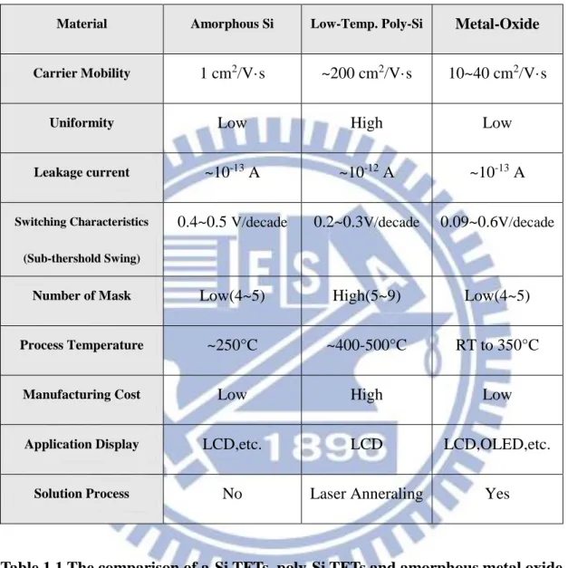
Table 1.1 The comparison of a-Si TFTs, poly-Si TFTs and metal oxide TFTs……….7
Table 1.2 The evolution of CMOS technology requirements (ITRS 2005)………..8
Table2.1 The experimental flow path……….17
VIII
Figure Captions
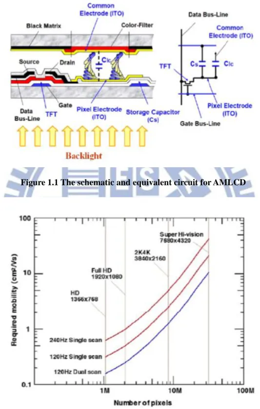
Figure 1.1 The schematic and equivalent circuit for AMLCD ... 9
Figure 1.2 Graphical summary of required carrier mobility for future displays ... 9
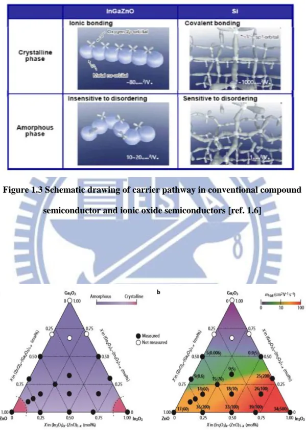
Figure 1.3 Schematic drawing of carrier pathway in conventional compound semiconductor and ionic oxide semiconductors ... 10
Figure 1.4 (a) Amorphous formation and (b) electron transport properties of In2O3-Ga2O3-ZnO thin films ... 10
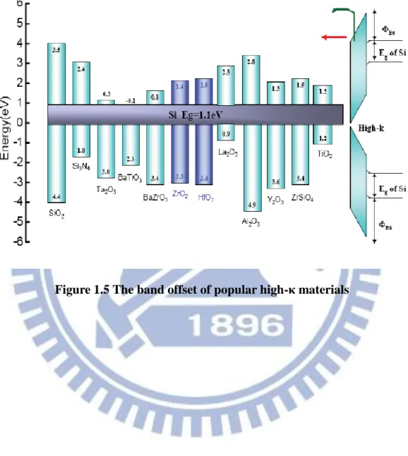
Figure 1.5 The band offset of popular high-κ materials ... 11
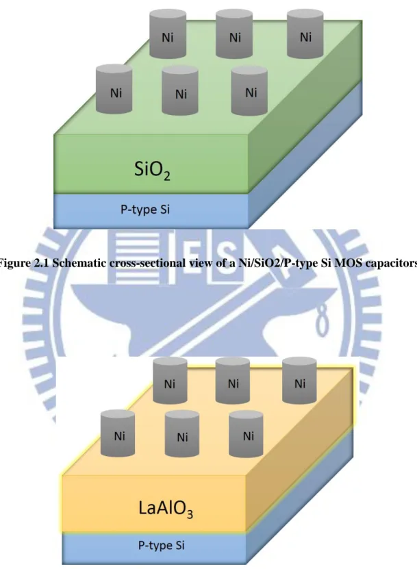
Figure 2.1 Schematic cross-sectional view of a Ni/SiO2/P-type Si MOS capacitors ... 19
Figure 2.2 Schematic cross-sectional view of a Ni/LaAlO3/P-type Si MOS capacitors... 19
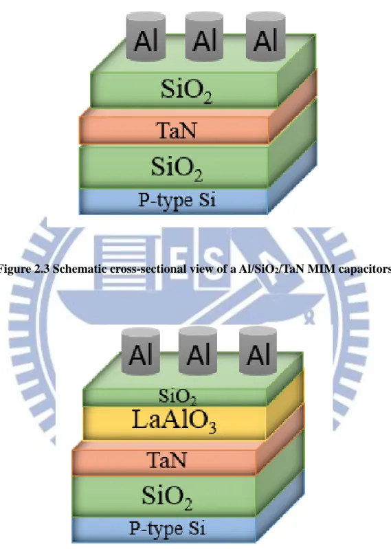
Figure 2.3 Schematic cross-sectional view of a Al/SiO2/TaN MIM capacitors ... 20
Figure 2.4 Schematic cross-sectional view of a Al/LaAlO3/TaN MIM capacitors ... 20
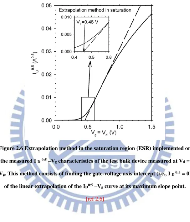
Figure 2.5 Schematic cross-sectional view of a-IGZO TFT with an inverted staggered bottom-gate structure ... 21
Figure 2.6 Extrapolation method in the saturation region (ESR) implemented on the measured I D0:5 –Vg characteristics of the test bulk device measured at Vd = Vg. This method consists of finding the gate-voltage axis intercept (i.e., I D 0:5 = 0) of the linear extrapolation of the ID0:5 –Vg curve at its maximum slope point. ... 22
Figure 3.1 C-V characteristics of Ni/SiO2/p-type Si MOS capacitors in 100KHZ ... 26
Figure 3.2 C-V characteristics of Ni/SiO2/p-type Si MOS capacitors in 300KH ... 26
Figure 3.3 C-V characteristics of Ni/LaAlO3/p-type Si MOS capacitors in 100KHZ... 27
Figure 3.4 C-V characteristics of Ni/LaAlO3/p-type Si MOS capacitors in 300KHZ... 27
IX
Figure 3.6 C-V characteristics of Al/SiO2/TaN MIM capacitors ... 30
Figure 3.7 C-V characteristics of Al/SiO2-LaALO3/TaN MIM capacitors ... 30
Figure 3.8 I-V characteristics of Al/SiO2/TaN MIM capacitors... 31
Figure 3.9 I -V characteristics of Al/SiO2-LaALO3/TaN MIM capacitors ... 31
Figure 3.10 ID-VD characteristics of a-IGZO TFTs ... 32
Figure 3.11 ID-VG characteristics of a-IGZO TFTs ... 32
Figure 3.12 The threshold voltage of a-IGZO TFTs Determinated by the extrapolation method in the saturation region ... 33
1
Chapter 1
Introduction
1.1 General Background of Thin-Film Transistor (TFT)
With fast growth of consumer electronic market, the displays with light weight, low power consumption, high resolution and high electrical performance have been substantially implemented to various commercial electronic products. At present, thin-film transistor (TFT) device technologies are widely used in flat-panel displays. The TFT has been widely used as switching device and current driving device in liquid crystal display (LCD) and organic light emitting diode display (OLED). [ref 1.1-1.3] In LCDs, the function of TFT is to control the bias between pixel electrode and common electrode (the schematic diagram is shown in Figure 1.1). The electrical field on liquid crystal cell orients the liquid crystal molecules to determinate the gray scale of each pixel. In OLEDs, the pixel circuit is composed of one switching TFT and one driving TFT. The OLED is integrated with the driving TFT directly and the brightness of the OLED is proportional to the amount of current. Therefore, a uniform and stable driving current is important to the image performance of LCDs and OLEDs. In general, the active layer of TFT is silicon-based material such as amorphous silicon (a-Si) and poly-crystalline silicon (poly-Si). There are many advantages for active matrix flat-panel displays application in amorphous silicon (a-Si), such as low fabrication temperature、 low manufacturing cost and good device uniformity; however, the critical issues include the low carrier mobility (~ 1 cm2/Vs) and poor stability. Compared to a-Si TFTs, low temperature poly-Si TFTs (LTPS TFTs) have a higher electron mobility and driving current which allows the smaller device dimensions to increase aperture ratio and luminance in one pixel. [ref 1.4] And the LTPS TFT is suitable for the high-resolution,
2
compact size active matrix display. However, the poor uniformity caused by grain boundary in Poly-silicon channel over a large area has been expected not to be promising in high-level yield for manufacturability. In addition, more masks during fabrication process require more cost.
As the panel size and the resolution of digital television increase, switching devices with higher electron mobility are required to decrease the charging time for each pixel and the RC delay in signal lines. It is estimated that the electron mobility over 3 cm2 / Vs is required for driving the ultrahigh-resolution (7680×4320) TV at 120-Hz frame rate. The required mobility will be even higher for displays with higher resolution 、 faster frame rate and a larger panel size (as shown in Figure 1.2). [ref 1.5] In order to combine the good uniformity of a-Si and the high carrier mobility of
poly-Si TFTs, the amorphous metal-oxide TFTs are developed to reach the superior electrical properties such as high carrier mobility、good uniformity、low process temperature and low manufacturing cost (the comparison of a-Si、poly-Si and metal-oxide material is shown in Table 1.1).
1.2 Overview of Amorphous Metal Oxide Semiconductor
Thin Film Transistors (AOS TFTs)
Recently, TFTs with active layers of metal oxide semiconductors, such as ZnO and amorphous InGaZnO (a-IGZO), have attracted considerable attention for the application in next generation display industry. [ref 1.6, 1.7] Because of amorphous
structure and wide band gap (~ 3.3eV for ZnO-based material), the AOS TFTs exhibits excellent transparent and good uniformity, and moreover, the AOS material can exhibit large carrier mobility (> 10 cm2/Vs) which is much higher than a-Si (~ 1 cm2/Vs).
3
Unlike the conventional a-Si TFT with poor carrier transport properties due to the chemical bonds in the covalent semiconductors are made of p or sp3 orbitals with strong spatial directivity. The conduction band minimum (CBM) of metal-oxides material are made of spherically extended s orbital of metal cations and their overlaps with neighboring metal s orbital and are not affected appreciably by the disordered amorphous structure. Therefore, the carrier transport in the conduction band is insensitive to the local structural randomness (as shown in Figure 1.3).
In the development of metal-oxide semiconductor TFTs, the carrier concentration of semiconductor is an important feature and ZnO material was investigated in the previous researches since this material is known as a good transparent-conducting-oxide (TCO) material, containing high density of mobile electrons even in nominally un-doped states. Therefore, the high carrier concentration makes ZnO difficult to control the channel conductance and threshold voltage, which often results in the device instability. Furthermore, the un-doped ZnO can easily form crystalline films even the deposition process is at room temperature. This phenomenon is widely observed in many metal-oxide materials and this issue makes it difficult to obtain amorphous phases. Therefore, the binary oxide compounds such as In-Zn-O 、In-Ga-O and Ga-Zn-O were developed to form amorphous phases if the mixing ratio between the oxide and the metal exceeds a certain threshold value (as shown in Figure 1.4 (a)). Generally, the mix of two or more cations with different sizes and ionic charges is effective to enhance the formation of amorphous phase and suppress the crystallization. Therefore, AOSs are usually multi-component systems and this phenomenon implies that a rich variety of AOS materials can be found in the future.
The Indium, Gallium and Zinc are the major components of good transparent conducting oxides since their unoccupied s orbital form the electron transport paths
4
resulting in good electron mobility in AOSs. To further investigate the role of these ions, it is useful to compare systems such as InO、GaO and ZnO. [ref 1.8] As seen in Figure 1.4 (b), although the mobility of Indium doping material (InZnO) is higher than the ZnO and Gallium doping material (InGaZnO) since the spherically s orbital of Indium is larger than Zinc, it is difficult to maintain the level of low electron concentration required for TFTs (e.g. far below 1017 cm–3). According to the first-principles density-functional theory, [ref 1.9] the Ga–O bonds are much stronger than Zn–O and In–O bonds indicating that the incorporation of gallium suppresses the formation of oxygen deficiencies which generates the mobile electrons. However, too much gallium content will deteriorate the electron mobility. Therefore, an appropriate amount of stabilizer ions doping in ZnO will not only form a strong chemical bond but exhibit excellent performance for the application of AOS TFTs. Although there are many advantages for AOS TFTs compared with the traditional Si-based TFTs, some stability and reliability issues need to be overcome for the application in LCDs and OLEDs since the AOS material is very sensitive to bias stress、light illumination、temperature and ambient environment.
1.3 Overview of high-κ gate dielectrics
The gate leakage current through the gate oxide increases significantly because direct tunneling is the primary conduction mechanism in down-scaling CMOS technologies. In order to reduce the leakage current related higher power consumption in highly integrated circuit and overcome the physical thickness limitation of silicon dioxide, the conventional SiO2 will be replaced with high dielectric constant (high-κ) materials as the gate dielectrics beyond the 65 nm technology mode [ref 1.10~1.15]. Therefore, the engineering of high-κ gate dielectrics have attracted great attention and
5
played an important role in VLSI technology. Although high-κ materials often exhibit smaller bandgap and higher defect density than conventional silicon dioxide, using the high-κ gate dielectric can increase efficiently the physical thickness in the same effective oxide thickness (EOT) that shows lower leakage characteristics than silicon dioxide by several orders without the reduction of capacitance density [ref 1.11~1.14]. Finally, according to the ITRS (International Technology Roadmap for Semiconductor) [ref 1.16], the suitable gate dielectrics must have κ value more than 8 for 50-70 nm technology nodes and that must be more than 15 when the technology dimension less than 50 nm. Figure 1.5 and Table 1.2 show the evolution of CMOS technology requirements.
1.4 Motivation
After some references demonstrated the transparent and flexible TFTs using novel amorphous indium–gallium–zinc oxide (a-IGZO), the a-IGZO TFTs have attracted a lot of attention for potential application in high drive current and large-area display with a low cost. This high transistor current is particularly required to drive high-resolution active-matrix organic light-emitting diode displays. Compared to the Si-based counterpart, a-IGZO TFTs can provide the merits of both amorphous-Si and polycrystalline-Si TFTs, i.e., even in the amorphous phase, a-IGZO TFTs still exhibit high mobility comparable with polycrystalline-Si TFTs, and the amorphous property of IGZO channel also helps to reduce the nonuniformity of mobility and threshold voltage (Vt ). To improve the device performance, low Vt and small subthreshold swing (S.S.)
are required. These can be achieved by controlling the device process, such as oxygen partial pressure, deposition pressure, channel thickness, IGZO composition, and anneal temperature etc. Incorporating high-κ gate dielectric into TFT provides alternative solution to reach these goals. In this study, we report the low-operating-voltage
a-6
IGZOTFT using high-κ LaAlO3 and SiO2 gate dielectric bilayer structure.
1.5 Organization of this Thesis
This thesis is divided into four chapters. In Chapter 1, a brief review from the material properties and device properties of the Thin-Film Transistor and Amorphous
Metal Oxide Semiconductor TFTs for the application in flat panel display and High-κ Gate Dielectrics technologies is given.
In Chapter 2, fabrication procedures and extracting methods of device parameters
for amorphous oxide TFTs are introduced. The measurement setups employed for device characterization are also presented in this chapter.
In Chapter 3, we present the device characteristics, including µFE, S.S., Vt, etc. and make a discussion.
7
Material Amorphous Si Low-Temp. Poly-Si Metal-Oxide
Carrier Mobility 1 cm2/V·s ~200 cm2/V·s 10~40 cm2/V·s
Uniformity Low High Low
Leakage current ~10-13 A ~10-12 A ~10-13 A
Switching Characteristics (Sub-thershold Swing)
0.4~0.5 V/decade 0.2~0.3V/decade 0.09~0.6V/decade
Number of Mask Low(4~5) High(5~9) Low(4~5)
Process Temperature ~250°C ~400-500°C RT to 350°C
Manufacturing Cost Low High Low
Application Display LCD,etc. LCD LCD,OLED,etc.
Solution Process No Laser Anneraling Yes
Table 1.1 The comparison of a-Si TFTs, poly-Si TFTs and amorphous metal oxide TFTs
8
9
Figure 1.1 The schematic and equivalent circuit for AMLCD
Figure 1.2 Graphical summary of required carrier mobility for future displays [ref. 1.5]
10
Figure 1.3 Schematic drawing of carrier pathway in conventional compound semiconductor and ionic oxide semiconductors [ref. 1.6]
Figure 1.4 (a) Amorphous formation and (b) electron transport properties of In2O3-Ga2O3-ZnO thin films [ref. 1.6]
11
Figure 1.5 The band offset of popular high-κ materials
12
Chapter 2
Fabrication and Characterization
We will introduce the detailed fabrication process flows and electrical measurements of all devices, including capacitors and a-IGZO TFTs. Table2.1 is the process flow for experiments. The electric properties were characterized by HP4155B semiconductor parameter analyzer. Table2.2 shows my experimental conception.
2.1 Process Flow of Capacitors
In this section we fabricated two different structure capacitors. One is metal– insulator–semiconductor (MOS) capacitors, another is metal–insulator–metal (MIM) capacitors.
The metal–insulator–semiconductor capacitors were fabricated on p-type Si substrate after RCA cleaning process. First a 30-nm LaAlO3 and 10-nm SiO2 gate dielectrics were deposited by PVD at room temperature, followed by a 400 ◦C O2 annealing for 10 min. Then, 35-nm Ni top electrodes were deposited and patterned bymetal masks. The schematic diagram of the metal–insulator–semiconductor capacitors was shown in Figure2.1 and Figure2.2. The metal–insulator–semiconductor capacitors were also fabricated side-by-side to characterize the κ value of capacitors and insulator’s quality.
The metal–insulator–metal capacitors were fabricated on the insulated SiO2/Si substrate. A 35nm TaN was first deposited by DC sputtering as bottom electrode. Next, a 40nm SiO2 dielectric was deposited by PVD at room temperature, followed by a 400◦C O2 annealing for 10 min as the insulator layer. In another condition, a 30nm LaAlO3 dielectric was deposited, followed by a 400◦C O2 annealing for 10 min. And then, a
13
10nm SiO2 dielectric was deposited, followed by a 400◦C O2 annealing for 10 min again. Finally, 350nm Al top electrodes were deposited and patterned in all conditions. The schematic diagram of the metal–insulator–metal capacitors was shown in Figure 2.3
and Figure 2.4.The metal–insulator–metal capacitors were also fabricated side-by-side to characterize the gate capacitance and leakage current.
2.2 Process Flow of a-IGZO TFTs
Our a-IGZO TFTs devices were fabricated on the insulated SiO2/Si substrate. A 35nm TaN was first deposited by DC sputtering. After gate patterning, A 30nm LaAlO3 gate dielectric was deposited by PVD at room temperature, followed by a 400◦C O2 annealing for 10 min. Then, a 10nm SiO2 gate dielectric was deposited by PVD at room temperature, followed by a 400◦C O2 annealing for 10 min again. The gate dielectric is preferred to form by PVD for its low process temperature, particularly when a plastic substrate is used [ref 2.1~2.2]. Next, 40nm IGZO channel layer was deposited by sputtering from a ceramic IGZO target (In2O3 : Ga2O3 : ZnO = 1 : 1 : 1) in a gas mixture with 30 sccm O2 and 24 sccm Ar. Finally, 350 nm Al were deposited as source/drain electrodes and annealed at 400◦C under N2 ambient for 10 min. Here, metal masks were used to pattern the device. The schematic diagram of the a-IGZO TFTs was shown in
Figure 2.5.
2.3 Methods of Device Parameter Extraction
2.3.1 Determination of the Threshold Voltage
Several methods are used to determinate the threshold voltage (VT) which is the
most important parameter of the semiconductor devices. The threshold voltage is defined by extrapolation method in the saturation region in this dissertation. The ESR (extrapolation method in the saturation region) method determines the threshold voltage
14
from the gate voltage axis intercept of the ID0:5sat–Vg characteristics linearly extrapolated at its maximum first derivative (slope) point as illustrated in Figure 2.6
The value of VT(sat) which is calculated for the present device results to be 0.46 V. [ref 2.3~2.6]
2.3.2 Determination of the Field-Effect Mobility
The μFE (field-effect mobility) is determined from the transconductance (gm) at low drain voltage. The transfer characteristics of TFTs are similar to the conventional MOSFETs, so the first order I-V relation in the bulk Si MOSFETs can be applied to the TFTs expressed as:
𝐈
𝒅=
𝑾 𝑳µ
𝒆𝒇𝒇𝐂
𝒐𝒙[(
𝐕
𝒈-
𝐕
𝒕)
𝐕
𝒅-𝟏 𝟐
𝑽
𝒅 𝟐]
(1) Where, W is channel width, L is channel length,Cox is the gate oxide capacitance per unit area (F/cm2)
Vt is the threshold voltage,
If Vd is so much smaller than Vg-Vt (i.e. Vd << Vg-Vt) & Vg>Vt, the drain current can be
approximated as:
𝐈
𝒅=
𝑾𝑳
µ
𝒆𝒇𝒇𝐂
𝒐𝒙[(
𝐕
𝒈-
𝐕
𝒕)
𝐕
𝒅]
(2) Furthermore, the transconductance (gm) is defined as:𝐠
𝒎=
𝛛𝑰𝒅𝛛𝑽𝒈
(3) Thence, the field-effect mobility can be obtained by:
µ =
𝑳15
2.3.3 Determination of the Sub-threshold Swing
Sub-threshold swing (S.S.) is a typical parameter to describe the gate control ability for the device. Furthermore, the parameter S.S is related with the interface states(Nit) for the TFT device directly as follow:
S.S. = (
𝒌𝑻𝒒
)
𝐥𝐧 𝟏𝟎 (𝟏 +
𝒒𝑵𝒊𝒕
𝑪𝒐𝒙
)
(5) where kT is the thermal energy and Cox is the gate insulator capacitance.From eq. (5), decreasing in the Nit can be obtained the smaller S.S. The S.S. should be independent of drain voltage and gate voltage. Nevertheless, in reality, S.S. might increase with drain voltage due to short-channel effects such as charge sharing, avalanche multiplication, and punch through-like effect. And S.S. can be lessened by substrate bias since it is affected by the total trap density including interfacial trap density and bulk density. In this study, S.S. was defined as the gate voltage required to decrease the threshold current by one orders of magnitude (from 10-9A to 10-10A). The threshold current was specified to be the drain current when the gate voltage is equal to Vt.
2.4 Measurement Setup
In this study, the devices were characterized by current–voltage ( I–V ) and capacitance–voltage ( C–V ) measurements using 4155B semiconductor parameter analyzer and Agilent E4980A precision LCR meter, respectively.
In the section of metal–insulator–semiconductor capacitors, we did capacitance– voltage measurement from the typical top electrode -to-ground bias which was swept forward from V = 2 V to V = -4 and then reverse from V = -4 V to V = 2 V in 100,300 and500KHZ frequency. In current–voltage measurement, the typical top electrode -to-ground bias was swept from V = 0 V to V = 2 V and V = 0 V to V = -2 V.
-to-16
ground bias which was swept from V = 2 V to V = -2 V and current–voltage measurement that the typical top electrode -to-ground bias was swept from V = 0 V to V = 2 V and V = 0 V to V = -2 V in the section of metal–insulator–metal capacitors. Finally, we did IDS-VGS measurement that the typical drain-to-source bias was swept from VGS = -0.5 V to VGS = 2 V, VDS= 0 to VDS= 1 V and IDS-VDS measurement that the typical drain-to-source bias was swept from VDS = 0 V to VDS = 2 V, VGS= 0V to VGS= 1 V.
17
18
Table2.2 The experimental conception in this study
What’s the quality
about SiO
2and
LaAlO
3MIM Capacitors
Fabrication
Conclusion
a-IGZO TFTs
Fabrication
19
Figure 2.1 Schematic cross-sectional view of a Ni/SiO2/P-type Si MOS capacitors
Figure 2.2 Schematic cross-sectional view of a Ni/LaAlO3/P-type Si MOS
20
Figure 2.3 Schematic cross-sectional view of a Al/SiO2/TaN MIM capacitors
21
Figure 2.5 Schematic cross-sectional view of a-IGZO TFT with an inverted staggered bottom-gate structure
22
Figure 2.6 Extrapolation method in the saturation region (ESR) implemented on the measured I D0:5 –Vg characteristics of the test bulk device measured at Vd =
Vg. This method consists of finding the gate-voltage axis intercept (i.e., I D 0:5 = 0)
of the linear extrapolation of the ID0:5 –Vg curve at its maximum slope point.
23
Chapter 3
Experimental Results and Discussion
3.1 Metal–Insulator–Semiconductor Capacitors
3.1.1 Analyzing C-V curves of SiO2 MOS and LaAlO3 MOS Capacitors
Figure 3.1 shows capacitance density-voltage (C-V) characteristics. A voltage shift of 1.2V for the SiO2 MOS capacitors during forward and reverse swept in 100KHZ was observed. Figure 3.3 shows capacitance density-voltage (C-V) characteristics. A voltage shift of 0.4V for the LaALO3 MOS capacitors during forward and reverse swept in 100KHZ was observed. Clearly, the voltage shift of SiO2 MOS was larger than LaAlO3 MOS. We had known that the quality of SiO2 insulator layer is poor because the SiO2/Si interface state was so rough that a lot of carriers were trapped at interface and oxide layer had many defects to trap charges. On the other hand, in Figure 3.1 and
Figure 3.2, compared with the C-V curves from 100KHZ to 300KHZ, it indicates that the flat-band voltage has been shifted from -0.2 V to -0.8 V. It can be seen that the metal/interface may be also poor to change the flat-band voltage. since the SiO2 insulator layer was deposited by dual E-GUN evaporation system and just followed by a low temperature as 400◦C O2 annealing for 10 min, it causes poor quality for SiO2 layer but not for LaAlO3 layer. Besides, the defects of MOS capacitors was shown as
Figure 3.5.
3.1.2 Summary
The SiO2 MOS capacitor has a large flat band voltage shift in forward and reverse swept measurements and the flat-band voltage is changed from -0.2 V to -0.8 V in frequency-varied measurement. The poor quality for SiO2 layer is related to the low
24
temperature PDA process and E-GUN evaporation system.
3.2 Metal–Insulator–Metal Capacitors
3.2.1 C-V characteristics of SiO2 MIM and LaAlO3/SiO2MIM Capacitors
The capacitance density-voltage (C-V) characteristics of the SiO2 MIM capacitors are shown in Figure 3.6. Figure 3.7 shows the capacitance density-voltage (C-V) characteristics of the LaAlO3/SiO2 MIM capacitors. The average capacitance density of SiO2 MIM capacitors and LaAlO3/SiO2 MIM capacitors are about 0.31µf/cm2,and 0.43µf/cm2, respectively The capacitance density of LaAlO3/SiO2 MIM capacitors is higher than SiO2 MIM capacitors. We can know that the higher capacitance density can decrease Vt and S.S. from eq. (6) and eq. (7).
S.S. = (
𝒌𝑻 𝒒)
𝐥𝐧 𝟏𝟎 (𝟏 +
𝒒𝑵𝒊𝒕 𝑪𝒐𝒙)
(6)𝑽
𝒕≡ 𝑽
𝑭𝑩+ 𝟐∅
𝑩+
√𝟐𝒒∈𝒔𝑵𝑨𝟐∅𝑩 𝑪𝒐𝒙(7)
3.2.2 I-V characteristics of SiO2 MIM and LaAlO3/SiO2MIM Capacitors
Figure 3.8 and Figure 3.9 show the current-voltage (I-V) characteristics of SiO2 MIM and LaAlO3/SiO2 MIM capacitors. Here, the leakage current of LaAlO3/SiO2 MIM capacitors is smaller than that of the SiO2 MIM capacitors, indicating that the SiO2 layer has a lot of defects deposited by dual E-GUN evaporation system and low temperature annealing treatment. The small leakage current can reduce the power consumption which plays an important role in green power devices.
3.3 Characteristics of a-IGZO TFTs
Our a-IGZO TFTs device has a channel length of 50 um and width of 500 um, respectively. The output ID–VD characteristics of the high-κ LaAlO3/SiO2 a-IGZO TFT
25
is shown in Figure 3.10. Well-behaved transistor characteristics were observed even under a low operation voltage of 1 V, which is important for low-power application.
Figure 3.11 shows the transfer ID–VG characteristics of the high-κ LaAlO3/SiO2 a-IGZO TFT. A low Vt of 0.5V was determined from the linear I D1/2 versus VG plot as shown in Figure 3.12. Low S.S. of 95 mV/dec is reached. Such small S.S. is essential to turn on the transistor fast at low voltage. The acceptable µFE mobility of 3.08cm2/V.s is obtained simultaneously.The gm and mobility are shown in Figure 3.13 This better performance is attributed to the high gate capacitance density, the larger conduction band offset for SiO2 / IGZO than that of LaAlO3/IGZO and good a-IGZO material.
26 -4 -3 -2 -1 0 1 2 0.0 5.0x10⁻² 1.0x10⁻¹ 1.5x10⁻¹ 2.0x10⁻¹ 2.5x10⁻¹ 3.0x10⁻¹ 3.5x10⁻¹ 4.0x10⁻¹ forward reverse Cap ac it ance Density ( F /cm 2 ) Voltage (V) deltaV=1.2V 100KHZ @VFB= - 0.2V
Figure 3.1 C-V characteristics of Ni/SiO2/p-type Si MOS capacitors in 100KHZ
-4 -3 -2 -1 0 1 2 0.0 5.0x10⁻² 1.0x10⁻¹ 1.5x10⁻¹ 2.0x10⁻¹ 2.5x10⁻¹ 3.0x10⁻¹ 3.5x10⁻¹ @VFB= - 0.8V 300KHZ forward reverse Cap ac it ance Density ( F /cm 2 ) Voltage (V) deltaV=0.84V
27 -4 -3 -2 -1 0 1 2 0.0 5.0x10⁻² 1.0x10⁻¹ 1.5x10⁻¹ 2.0x10⁻¹ 2.5x10⁻¹ 3.0x10⁻¹ 3.5x10⁻¹ 4.0x10⁻¹ 4.5x10⁻¹ 5.0x10⁻¹ 5.5x10⁻¹ forward reverse Cap ac it ance Den sit y( F /cm 2 ) Voltage (V) deltaV=0.4V
Figure 3.3 C-V characteristics of Ni/LaAlO3/p-type Si MOS capacitors in
100KHZ -4 -3 -2 -1 0 1 2 0.0 5.0x10⁻² 1.0x10⁻¹ 1.5x10⁻¹ 2.0x10⁻¹ 2.5x10⁻¹ 3.0x10⁻¹ 3.5x10⁻¹ 4.0x10⁻¹ 4.5x10⁻¹ 5.0x10⁻¹ 5.5x10⁻¹ forward reverse Cap ac it ance Density ( F /cm 2 ) Voltage (V) deltaV=0.36V
28
29
30 -2.0 -1.5 -1.0 -0.5 0.0 0.5 1.0 1.5 2.0 2.0x10⁻¹ 2.5x10⁻¹ 3.0x10⁻¹ 3.5x10⁻¹ 4.0x10⁻¹ 4.5x10⁻¹ 5.0x10⁻¹ Cap ac it ance Density ( F /cm 2 ) Voltage (V)
Figure 3.6 C-V characteristics of Al/SiO2/TaN MIM capacitors
-2.0 -1.5 -1.0 -0.5 0.0 0.5 1.0 1.5 2.0 3.0x10⁻¹ 3.5x10⁻¹ 4.0x10⁻¹ 4.5x10⁻¹ 5.0x10⁻¹ 5.5x10⁻¹ 6.0x10⁻¹ Cap ac it ance Density ( F /cm 2 ) Voltage (V)
31 -2.0 -1.5 -1.0 -0.5 0.0 0.5 1.0 1.5 2.0 10-12 10-11 10-10 10-9 10-8 10-7 10-6 Cu rr ent ( A) Voltage (V)
Figure 3.8 I-V characteristics of Al/SiO2/TaN MIM capacitors
-2.0 -1.5 -1.0 -0.5 0.0 0.5 1.0 1.5 2.0 10-13 10-12 10-11 10-10 10-9 10-8 10-7 10-6 Cu rr ent ( A) Voltage (V)
32 0.0 0.1 0.2 0.3 0.4 0.5 0.6 0.7 0.8 0.9 1.0 0.0 0.2 0.4 0.6 0.8 1.0 1.2
Drai
n Cu
rr
ent
(
A
)
Drain Voltage (V)
Vg=0V Vg=0.2V Vg=0.4V Vg=0.6V Vg=0.8V Vg=1.0VFigure 3.10 ID-VD characteristics of a-IGZO TFTs
33 -0.4 -0.2 0.0 0.2 0.4 0.6 0.8 1.0 1.2 1.4 1.6 0.0000 0.0002 0.0004 0.0006 0.0008 0.0010 0.0012 0.0014 0.0016 0.0018
Sqrt(D
ra
in Cu
rr
ent
)
(A
0.
5
)Gate Voltage
(V
)
@V
t= 0.5V
Figure 3.12 The threshold voltage of a-IGZO TFTs Determinated by the extrapolation method in the saturation region
-0.4 -0.2 0.0 0.2 0.4 0.6 0.8 1.0 1.2 1.4 1.6 0.000000 0.000001 0.000002 0.000003 0.000004 0.000005 0.000006 0.000007 Gate Voltage (V) g m 0.0 0.2 0.4 0.6 0.8 1.0 1.2 1.4 1.6 1.8 2.0 2.2 2.4 2.6 2.8 3.0 3.2 3.4 m o b ilit y (cm 2 /Vs )
34
35
Chapter 4
Conclusion
In conclusion, incorporating LaAlO3 /SiO2 as gate dielectrics, the IGZO TFTs show a small S.S. of 95 mV/dec, a low Vt of 0.5 V, and an acceptable μFE of 3.08 cm2/V∙ sec at operation voltage as low as 1.7 V. These good performances were related to the high gate capacitance density by introducing the high-κ LaAlO3 dielectric. The present results show that these low operation voltage IGZO TFTs with LaAlO3 /SiO2 as gate dielectrics have high potential for future high speed and low power applications.
Since the IGZO TFT performances still need improvements, we will do more work to enhance the device characteristics in the future.
36
References
[1.1]: Y.C. Wu , T.C. Chang, P. T. Liu, C.S. Chen, C.H. Tu, H. W. Zan, Y. H. Tai, and C. Y. Chang,” Effects of channel width on electrical characteristics of polysilicon TFTs with multiple nanowire channels,” IEEE Trans. Elec. Dev, vol.52, no.10, p.2343, (2005).
[1.2]: Y. Matsueda, R. Kakkad, Y. S. Park, H. H. Yoon, W. P. Lee, J. B. Koo, and H. K. Chung,” 2.5-in AMOLED with integrated 6-bit gamma com- pensated digital data driver,” in SID Tech. Dig. p.1116, (2004).
[1.3]: H. Kuriyama, S. Kiyama, S. Noguchi, T. Kuahara, S. Ishida, T. Nohda, K. Sano, H. Iwata, S. Tsuda, and S. Nakano, “High mobility poly-Si TFT by a new excimer laser annealing method for large area electronics,” IEDM Tech. Dig, p. 563, (1991).
[1.4]: J.-H. Lee, W.-J. Nam, B.-K. Kim, H.-S. Choi, Y.-M. Ha, and M.-K. Han, “A new poly-Si TFT current-mirror pixel for active matrix organic light emitting diode,” IEEE
Electron Device Lett., vol. 27, no. 10, pp. 830–833, Oct. (2006)
[1.5]: T. Kamiya, K. Nomura and H. Hosono. “Present status of amorphous In-Ga-Zn-O thin-film transistors”, Science and Technology of Advanced. Material, Vol. 11, pp. 044305, (2010).
[1.6]: K. Nomura, H. Ohta, A. Takagi, T. Kamiya, M. Hirano, and H. Hosono, “Room-temperature fabrication of transparent flexible thin-film transistors using amorphous oxide semiconductors,” Nature, vol. 432, no. 7016, pp. 488–492, Nov. (2004).
[1.7]: E. Fortunato, P. Barquinha, A. Pimentel, A. Goncalves, A. Marques, L. Pereira, and R. Martins, “Fully transparent ZnO thin-film transistor produced at room temperature,” Adv. Mater., vol. 17, no. 5, pp. 590–594, Mar. (2005).
37
[1.8]: T. Kamiya and H. Hosono. “Material characteristics and applications of transparent amorphous oxide semiconductors”, NPG Asia Material, Vol. 2, pp. 15-22, (2010).
[1.9]: T. Kamiya, K. Nomura, H. Hosono, “Origins of High Mobility and Low Operation Voltage of Amorphous Oxide TFTs: Electronic Structure, Electron Transport, Defects and Doping” J. Display Technol. 5, 273 (2009)
[1.10] M. Koyama, K. Suguro, M. Yoshiki, Y. Kamimuta, M. Koike, M. Ohse, C. Hongo and A. Nishiyama, “Thermally stable ultra-thin nitrogen incorporated ZrO2 gate dielectric prepared by low temperature oxidation of ZrN,” in IEDM Tech. Dig., pp. 20.3.1-20.3.4, 2001.
[1.11] E. P. Gusev, D. A. Buchanan, E. Cartier, A. Kumar, D. DiMaria, S. Guha, A. Callegari, S. Zafar, P. C. Jamison, D. A. Neumayer, M. Copel, M. A. Gribelyuk, H. Okorn-Schmidt, C. D Emic, P. Kozlowski, K. Chan, N. Bojarczuk, L. -A. Ragnarsson and Rons, “Ultrathin high-κ gate stacks for advanced CMOS devices,” in IEDM Tech. Dig., pp. 20.1.1-20.1.4, 2001.
[1.12] W. Zhu, T. P. Ma, T. Tamagawa, Y. Di, J. Kim, R. Carruthers, M. Gibson and T. Furukawa, “HfO2 and HfAlO for CMOS: thermal stability and current transport,” in IEDM Tech. Dig., pp. 20.4.1-20.4.4, 2001.
[1.13] L. Kang, K. Onishi, Y. Jeon, Byoung Hun Lee, C. Kang, Wen-Jie Qi, R. Nieh, S. Gopalan, R Choi and J. C. Lee, “ MOSFET devices with polysilicon on single-layer HfO2 high-κ dielectrics,” in IEDM Tech. Dig., pp. 35-38, 2000.
[1.14] Rino Choi, Chang Seok Kang, Byoung Hun Lee, K. Onishi, R. Nieh, S. Gopalan, E. Dharmarajan and J. C. Lee, “High-quality ultra-thin HfO2 gate dielectric MOSFETs with TaN electrode and nitridation surface preparation,” in IEDM Tech. Dig., pp. 15-16, 2001.
38
[1.15] Z. J. Luo, T. P. Ma, E. Cartier, M. Copel, T. Tamagawa and B. Halpern, “Ultra-thin ZrO2 (or silicate) with high thermal stability for CMOS gate applications,” in Symp. on VLSI Technology, pp. 135-136, 2001.
[1.16] International Technology Roadmap for Semiconductor, 2004.
[2.1] K. Nomura, H. Ohta, A. Takagi, T. Kamiya, M. Hirano, and H. Hosono,“Room-temperature fabrication of transparent flexible thin-film transistors using amorphous oxide semiconductor,” Nature, vol. 432, no. 7016,pp. 488–492, Nov. 2004.
[2.2] L. Pereira, P. Barquinha, E. Fortunato, R. Martins, D. Kang, C. J. Kim,H. Lim, I. Song, and Y. Park, “High k dielectrics for low temperature electronics,” Thin Solid
Films, vol. 516, no. 7, pp. 1544–1548,Feb. 2008.
[2.3] Schroeder DK. Semiconductor material and device characterization,2nd ed. New York: Wiley; 1998.
[2.4] Liou JJ, Ortiz-Conde A, Garc_ıa S_anchez FJ. Analysis and design of MOSFETs: modeling, simulation and parameter extraction. New York, USA: Kluwer Academic Publishers;1998.
[2.5] Haddara H. Characterization methods of submicronMOSFETs. New York, USA: Kluwer Academic Publishers;1996.
[2.6] A. Ortiz-Conde, F.J. Garc_ıa S_anchez, J.J. Liou, A. Cerdeira, M. Estrada, Y. Yue, “A review of recent MOSFET threshold voltage extraction methods,” in Microelectronics Reliability 42,pp.583–596,2002


![HPSH [ 氧化數平衡反應式係數 ]](data:image/gif;base64,R0lGODlhAQABAIAAAP///wAAACH5BAEAAAAALAAAAAABAAEAAAICRAEAOw==)