國立交通大學
電子工程學系 電子研究所碩士班
碩士論文
多晶鍺元件的研製與分析
Fabrication and Characterization of Poly-Ge Based Devices
研 究 生:張佑寧
指導教授:林鴻志 博士
黃調元 博士
多晶鍺元件的研製與分析
Fabrication and Characterization of Poly-Ge Based Devices
研 究 生:張佑寧 Student: Yu-Ning Chang 指導教授:林鴻志 博士 Advisors: Dr. Horng-Chih Lin 黃調元 博士 Dr. Tiao-Yuan Huang
國立交通大學
電子工程學系 電子研究所碩士班
碩士論文
A Thesis
Submitted to Department of Electronics Engineering & Institute of Electronics College of Electrical and Computer Engineering
National Chiao-Tung University in Partial Fulfillment of the Requirements
for the Degree of Master in
Electronic Engineering July 2009
Hsinchu, Taiwan, Republic of China
I
多晶鍺元件的研製與分析
研究生:張佑寧 指導教授:林鴻志 博士 黃調元 博士國立交通大學
電子工程學系 電子研究所碩士班
摘 要
在本論文研究中,我們探討了多晶鍺薄膜和鍺化鎳的材料特性。藉由不同形 式的結晶方法,由超高真空濺鍍系統沈積的非晶鍺會被轉變成多晶鍺薄膜。從固 相結晶法(SPC)的結果,我們發現在經過 500 ℃ 1 小時的退火處理後,非晶鍺會 轉變成多晶鍺且晶粒尺寸會達到飽和,不再隨退火時間的增加而增加尺寸。與 SPC 相比,金屬誘發結晶法(MIC)在鎳的幫助下可降低結晶溫度且獲得較大的晶 粒尺寸。而 MIC 除了可以增加薄膜的結晶性之外,亦可運用於摻雜的活化,也 就是金屬誘發摻雜活化(MIDA)技術。因為在 MIC 過程中,摻雜會因晶格重排而 進入取代位,所以 MIDA 可在低溫下進行摻雜的活化。金屬鍺化物的使用被認 為可以降低寄生電阻並解決較低的摻雜固態溶解度的問題,而我們發現形成鍺化 鎳的適合溫度為 300 ℃到 375 ℃。此外,在本論文中,我們也製作了五種元件, 從電性結果來看,我們發現多晶矽的存在可以增加多晶鍺薄膜的結晶性,而且當 多晶矽是被沈積在源極和汲極端的多晶鍺薄膜的下方時,多晶矽對電性的影響是 最明顯的。Fabrication and Characterization of Poly-Ge Based Devices
Student: Yu-Ning Chang Advisors: Dr. Horng-Chih Lin Dr. Tiao-Yuan Huang
Department of Electronics Engineering and Institute of Electronics National Chiao Tung University, Hsinchu, Taiwan
Abstract
In this study, material properties of poly-Ge thin films and Ni germanides were
investigated. The poly-Ge thin films were formed by different crystallization schemes
performed on a-Ge deposited by an ultra-high vacuum sputter. From the results of
solid-phase crystallization (SPC) method, we found that a-Ge is transformed into
poly-Ge at 500 ℃ for 1 hour annealing and then the grain size saturates. For
metal-induced crystallization (MIC) method, the crystallization temperature can be
reduced with the assistance of Ni and the grain size is bigger than that formed by SPC
method. In addition to enhanced crystallization, MIC can be applied to activate
dopants at low temperature, termed metal-induced dopant activation (MIDA), because
dopants will be rearranged into the substitutional sites during MIC process.
Germanide process is expected to reduce the parasitic resistance and alleviate the
issue of low dopant solid solubility. We found that the suitable temperature to form
NiGe is from 300 ℃ to 375 ℃. Besides, we also fabricate five types of devices in
this thesis. From the electrical characteristics, we discovered that poly-Si can increase
the crystallinity of poly-Ge and this apparent effect occurs when poly-Si is deposited
under the poly-Ge film at the S/D region.
Acknowledgment
寫到了這章節意味著論文已完成差不多了,能夠完成這本論文要感謝 的人太多了。首先,我要誠摯地感謝我的指導老師林鴻志博士和黃調元博 士。感謝兩位老師無私地指導我正確的研究態度與方法,在兩位老師的細 心指導下,這兩年來無論是在待人處事上、看問題的思考角度或是研究上 應有的態度,我都從老師們身上學到了很多。林博、黃老師真的很謝謝你 們對我的指導。 再來,我要感謝實驗室的學長姐、同學和學弟妹們。第一個要感謝的 是大師,謝謝你在一旁帶著我做實驗、不厭其煩地與我討論實驗上和量測 上遇到的問題,如果沒有你,我想現在這本論文應該還在難產中,真的很 謝謝你。感謝哲民、蘇博、徐博、蔡子儀等實驗室學長們,謝謝你們與我 討論實驗上遇到的問題以及對我實驗上幫助。接著要感謝跟我同梯的伙伴 們,政建,謝謝你時常跟我討論以及給我實驗上的幫助;gaygay,你是 ADTL 的強力活動股,謝謝你讓我們多了不少快樂的回憶;桀桀,被認為神似而 多次被認錯的經驗讓我印象深刻,謝謝你常跟我討論我在實驗上遇到的各 種疑問,阿嘎、君帆、瑄勻、阿 mo、maca、濤濤,謝謝你們這兩年來的 關照,和你們大家一起做實驗的那些日子很難忘,祝福大家都有一個自己 想要的未來。實驗室的小碩一們,最近才慢慢和你們變熟,祝你們未來一 年的實驗順利。 感謝小該、秉、承、sky、妹弟、顏、老古、米蟲、Eason、老余、逼 逼、wa、煙、家興、江伯、胖蔡、火龍果和 shiny 等我的同學朋友們,因 為有你們,讓我幾近一成不變的生活多了點變化,為平凡的日子增添不少 趣味和笑聲,能認識你們真好,謝謝你們,希望你們都能走在自己想走的 路上。 謝謝 NDL 的小姐:趙子綾、徐台鳳、蕭明娟、范庭瑋、李春杏、周 家如等以及 NDL 的工程師們,如果沒有你們在實驗上的幫助,我的實驗 很難順利的完成。 最後,獻給我親愛的家人,張呈芳先生、邱永娥女士以及兩位弟弟, 因為有你們的支持,我才能無所顧慮地求學,也才有這本論文的完成,謝 謝你們包容我這任性、不常回家孩子。 再一次謝謝所有人,因為有你們才會有這本論文,謝謝你們。 張佑寧 誌於風城 2009 年 7 月 IVCONTENTS
Abstract (Chinese)………I Abstract (English)………...II Acknowledgment (Chinese)...IV Contents………..……..V Figure Captions...VII Chapter 1 Introduction1-1 Overview………..1
1-1-1 Solid Phase Crystallization (SPC)………4
1-1-2 Metal Induced Crystallization (MIC)………...5
1-2 Motivation………6
1-3 Thesis Organization……….7
Chapter 2 Material Analysis
2-1 Material Analysis of SPC……….9
2-1-1 Sample Preparation………9
2-1-2 Results and Discussion………...10
2-2 The Material Analysis of MIC and MIDA……….12
2-2-1 Sample Preparation of MIC………12
2-2-2 Sample Preparation of MIDA……….13
2-2-3 Results and Discussion………...14
2-3 The Material Analysis of Germanides………...17
2-3-1 Sample Preparation of Germanides………18
2-3-2 Results and Discussion………...18
Chapter 3 Electrical Characteristics of Poly-Ge TFTs 3-1 Process Flow and Device Structures………..23
3-2 Measurement Setup for Electrical Characterization………..26
3-3 Fundamental Characteristics of Poly-Ge TFTs………...26
Chapter 4 Conclusions and Future Works
4-1 Conclusions………32 4-2 Future Works………..33 References………...35 Figures……….42 Vita………...68 VI
Figure Captions
Chapter 2
Fig. 2-1 XRD profiles of SPC samples at various annealing temperatures from 400 ℃ to 500 ℃ for 2 hours. The XRD intensity profile of fresh Ge film is shown as a reference. ………42
Fig. 2-2 XRD profiles of SPC samples annealed at 500 ℃ for various annealing times from 30 minutes to 6 hours. The XRD intensity profile of fresh Ge film is shown as a reference. ………43
Fig. 2-3 (a) shows the TEM cross-sectional view of poly-Ge film annealed at 500 ℃ for 1 hour. The circled area in the image indicates the grain size, and (b) presents the diffraction pattern of the poly-Ge film. ………44
Fig. 2-4 TEM cross-sectional view of poly-Ge film annealed at 500 ℃ for 6 hours. ………45
Fig. 2-5 AFM images of Ge films annealed at 500 ℃ for 1 hour for (a) without protection of oxide capping layer, and (b) with protection of capping layer during annealing………46
Fig. 2-6 The difference of sheet resistance between Ge film with oxide capping layer and without capping layer during annealing. ………47
Fig. 2-7 XRD profiles for Ni MIC in (a) and Al MIC in (b). ………48
Fig. 2-8 Comparison of XRD profiles between Ni MIC annealed at 350 ℃ for 1
hour and SPC at 500 ℃ for 1 hour. ………49
Fig. 2-9 TEM cross-sectional view of poly-Ge film formed by Ni MIC. …………49
Fig. 2-10 (a) The sheet resistance of three types (p-type, n-type, and undoped) MIDA samples annealed at 350 ℃ for 1 hour with different implanted dose. (b) The comparison of sheet resistance between thress types MIDA samples and thermally activated samples annealed at 350 ℃ for 1 hour and 500 ℃ for 1 hour, respectively. ………50
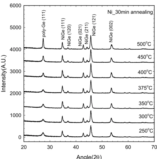
Fig. 2-11 The XRD spectra of the NiGe samples annealed at various temperature from 250 ℃ to 500 ℃. ………51
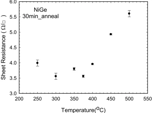
Fig. 2-12 The sheet resistance of the NiGe samples annealed at the temperature ranging from 250 ℃ to 500 ℃. ………52
Fig. 2-13 XRD spectra showing the poly-Ge(111) peak of the NiGe samples as a function of the temperature. The crystallite sizes estimated by using the Scherrer relation are presented in the inset. ………53
Fig. 2-14 AFM images of NiGe samples formed at (a) 300 ℃, (b) 400 ℃, (c) 450 ℃, and (d) 500 ℃ for 30 minutes annealing. ………54
Fig. 2-15 Cross-sectional SEM images of NiGe film formed at (a) 300 ℃ and (b) 500 ℃ for 30 minutes annealing. ………55
Fig. 2-16 The XRD profiles of as-deposited sample and the samples of nickel germanides annealed at various temperature from 250 ℃ to 500 ℃ for 30 minutes. ………56
Chapter 3
Fig. 3-1 The cross-sectional views of devices: (a) type A, (b) type B, (c) type C, (d)
type D, and (e) type E. ………57
Fig. 3-2 Process flow of device type A. ………58
Fig. 3-3 Process flow of device type B. ………59
Fig. 3-4 (a) Transfer and (b) output characteristics of device type A. ………60
Fig. 3-5 Comparison of transfer characteristics of device type A and E. …………61
Fig. 3-6 Comparison of XRD spectra of Ge-on-oxide and Ge-on-poly-Si after carrying out SPC. ………61
Fig. 3-7 Transfer characteristics of device type C. ………62
Fig. 3-8 Comparison of transfer characteristics of device type C and D. …………62
Fig. 3-9 Comparison of transfer characteristics of device type A and C. …………63
Fig. 3-10 (a) Transfer and (b) output characteristics of device type A after the plasma treatment. ………64
Fig. 3-11 Comparison of transfer characteristics of device type A before and after the plasma treatment. ………65
Fig. 3-12 (a) Transfer and (b) output characteristics of device type B. ………66
Fig. 3-13 Comparison of transfer characteristics of device type A and B. …………67
Chapter 1
Introduction
1-1 Overview
Moore's law has been a guideline for the semiconductor industry for over 30 years,
which predicted that the number of transistors will double every 18 months. To
sustain Moore's law, transistors have to be continuously scaled down along with
improved performances. However, as the feature size of the devices reaches the 32nm
technology node and beyond, conventional scaling methods for planar transistors face
more and more technological bottlenecks and fundamental challenges [1]. It requires
careful control of intricate lateral and vertical channel doping profiles including very
shallow source/drain (S/D) junctions, ultrathin gate dielectrics, and heavy doping to
suppress the subthreshold leakage current and the short-channel effect. Nevertheless,
some of the approaches aforementioned are in conflict with the objective of obtaining
high subthreshold slope, low series resistance, large drive current, high carrier
mobility, and low leakage current at low operating voltage as required by ITRS
roadmap [2]. Besides, as a result of absolute deteriorations due to longer spans and a
2
smaller wire cross-section as well as the relative deterioration of interconnects with
respect to transistors, scaling of transistors results in the increase of power
consumption and interconnect delay which leads to a serious performance bottleneck
[3]-[4]. Further, it is becoming increasingly difficult to achieve higher performance
devices through scaling down by virtue of excessive stand-by power accompanying
the scaling of transistors [4]. Therefore to further continue the scaling of silicon
complementary metal-oxide-semiconductor field-effect transistors (CMOSFETs), the
uses of alternative three-dimensional integrated circuits (3D-ICs) [3] at the
architecture level and higher carrier mobility channel materials at the device level are
considered to be the promising remedies to deal with interconnect and transistor
issues such as large power dissipation and delay, respectively [5]. Recently,
germanium (Ge) has attracted much attention due to its higher electron and hole
mobilities and lower effective mass over Si. Moreover, by virtue of its low melting
point, Ge is also appropriate for 3D-ICs which require low process temperature in
order not to damage the underlying interconnects and devices [4].
However, there are several drawbacks for using Ge as a channel material such as
the higher leakage current over Si due to its smaller band-gap, the S/D formation, and
the absence of stable native oxide as the gate dielectric [2], [6]. Even though Ge lacks
3
dielectrics as gate dielectric materials, such as GeON, HfO2, HfAlO, ZrO2, and Al2O3
[7]-[11], have been investigated, and very promising results have been demonstrated.
On the other hand, silicide process has been used widely in silicon-based
metal-oxide-semiconductor field-effect transistors (Si-MOSFETs) to reduce the
parasitic resistance and RC time delay for high performance demand. Therefore,
germanide process can improve the shortcoming of fast dopant diffusion during
activation [12] in Ge and low doapnt solubility [13], leading to lower S/D parasitic
resistance for achieving the desired device performance. Moreover, the self-aligned
germanide technology is indispensable for high speed transistors, similar to the
self-aligned silicide (Salicide) process used in Si-MOSFETs. Like nickel (Ni), which
is the most popular metal for silicide process in nano-scale CMOS manufacturing, Ni
germanide is considered to be the most potential candidate for Ge-MOSFET
applications. Besides the metal germanide technology, metal-induced dopant
activation (MIDA) [14] is proposed to alleviate the drawback of Ge nowadays.
For thin film transistor (TFT) applications, polycrystalline-Ge (poly-Ge) TFTs are
expected to realize the advanced system-on-panel (SOP) applications owing to their
higher carrier mobility and driving current. Moreover, the process temperature of
poly-Ge can be reduced due to their lower melting point over Si, and the
4
leading to cheaper cost. Up to present, there are several approaches for the fabrication
of the poly-Ge film, including solid-phase crystallization (SPC) [15], metal-induced
lateral crystallization (MILC)/metal-induced crystallization (MIC) [5], laser annealing
[16], and imprint-induced SPC [17]. More details about SPC and MIC will be
described as follows.
1-1-1 Solid Phase Crystallization (SPC)
Similar to the fabrication of poly-Si film for TFT applications, SPC is a common method to transform amorphous-Ge (a-Ge) into poly-Ge. The mechanism of SPC is
interpreted as a bond rearrangement process in the interface of the amorphous layer
and the crystalline layer where the breaking of bond is thermally activated at the
defect sites. There are several steps leading to a decrease in the total distortion energy
associated with the bond bending in the amorphous layer, and the activation energy of
SPC is given by the sum of the maximum distortion energy encountered during the
migration of dangling bond and the broken energy of bond [15], [18].
Like most solid-state transition, the phase transformation from amorphous state to
polycrystalline state consists of nucleation and crystallization steps. At first the
crystalline film can heterogeneously nucleate at the defect sites or the interfaces
5
then gradually enlarge until the two adjoining grains contact with each other which
forms a region called the grain boundary. However, the average grain size of poly-Ge
formed by SPC is relative small in comparison with poly-Si [19]-[20] so the carrier
transport in the poly-Ge film would encounter serious scattering effect; and more
grain boundaries, where abundant intra-grain strain bonds and dangling bonds exist,
are more likely to trap carriers. Not only would the carrier mobility be degraded, the
performance of devices would also be significantly influenced. Hence, several
approaches for enlarging the grain size are investigated such as two-step SPC [21] and
the insertion of thin Si layer between a-Ge layer and oxide layer [22].
1-1-2 Metal Induced Crystallization (MIC)
For TFTs and 3D-ICs applications, MIC is more suitable than SPC because the
process temperature of MIC is lower than that of SPC. The MIC growth is mainly
carried out by the following two kinds of metal groups: (1) Al-like metals such as Al,
Au, Ag, and Pb, and (2) Ni-like metals including Ni, Co, and Pd. The metals dissolved
in a-Ge are believed to weaken the bonding of Ge atoms in contact with metals and
then enhance the nucleation of crystalline Ge, leading to lower crystallization
temperature. The crystallization temperature of Al-like metals is higher than that of
6
the temperature is above the eutectic temperature, the Al-like metals will move toward
the a-Ge region and then form eutectic with Ge by the pseudo-eutectic reaction. After
the formation of the first eutectic layer, the metals continuously diffuse into the a-Ge
layer which has not yet been eutectic and leave the crystalline Ge phase behind [5],
[23]-[24]. For Ni-like metals, while the crystallization temperature is reached, the
metals migrate toward a-Ge region and then react with a-Ge to form germanides.
After the formation of first germanides layer, the metals continuously move toward
the a-Ge layer which has not become germanides yet and the Ge atoms that remain
behind attach to germanides template to form crystalline Ge [5], [25].
However, as a result of a large number of heterogeneous nuclei formed by the
assistance of metals leading to too many growth collisions and competitions, the grain
size of poly-Ge formed by MIC is small which will seriously degrade the performance
of device by (1) increasing the leakage current and power, (2) reducing the on-current,
and (3) degrading the subthreshold slope. Therefore, the approach of
self-nucleation-free MILC along with keeping the linear dimension of Ge smaller than
possible average grain size to obtain bigger grain is recently investigated and
discussed [5].
7
As described earlier in this chapter, since Ge possesses higher hole and electron
mobilities, smaller band-gap, and lower process temperature than Si, it is considered a
promising candidate to replace Si for high performance devices in the future. So far,
there are already comprehensive researches on Ge-MOSFETs fabricated on bulk Ge
and Ge-on-insulator (GOI) and very promising results have been achieved [26]-[28].
Nevertheless, there are relative few studies concerning poly-Ge for TFT applications.
Hence, the objective of this study is to investigate various material characteristics of
ultrahigh vacuum (UHV) sputtered Ge involving temperature of SPC, MIDA, and
germanide. After careful material analysis, optimal conditions are obtained and
utilized to fabricate poly-Ge TFTs, followed by detailed electrical analysis of the
transistors.
1-3 Thesis Organization
The organization of this thesis is divided into four chapters. In this chapter, a brief
overview and motivation are given. In Chapter 2, we briefly describe the preparation
of samples for analyzing material characteristics of Ge. Then the properties of MIC,
SPC, MIDA, and metal germanide are investigated and discussed. In Chapter 3, the
process flow for fabricating transistors is briefly presented, and the electrical
8
discussed. Finally, a concise summary of conclusion achieved in this thesis and some
Chapter 2
Material Analysis
2-1 Material Analysis of SPC
In this section, we will describe the process of sample preparation for SPC and then
the recrystallization temperature of SPC will be investigated and discussed.
2-1-1 Sample Preparation
The starting materials were p-type 150 mm Si(100) wafers with a 200 nm thick
thermal oxide layer. After standard cleaning, a 100 nm thick a-Ge film was deposited
on the SiO2 through an ultrahigh-vacuum Ge sputtering system with a base pressure
of 5 × 10– 8 Torr. To investigate the effect of the oxide capping layer, the reference
samples were free from the oxide capping layer while a TEOS oxide capping layer
was deposited onto the Ge film of the testing samples at 350 ℃ by plasma-enhanced
chemical vapor deposition (PECVD) system. Subsequently, all the samples were
annealed at 400 ℃ - 500 ℃ for times ranging from 0.5 h to 6 h in N2 ambient at
atmospheric pressure.
After subjecting to a buffered oxide etch (B.O.E) solution, the surface roughness
was studied by atomic force microscope (AFM), and the phase identification of Ge
film was carried out using X-ray diffraction (XRD) measurements in a θ-2θ geometry
with Cu Kα radiation (λ = 1.5418 ). The grain size of poly-Ge was estimated by
using high resolution transmission electron microscopy (HRTEM) on a
cross-sectional view of the poly-Ge film. o
A
2-1-2 Results and Discussion
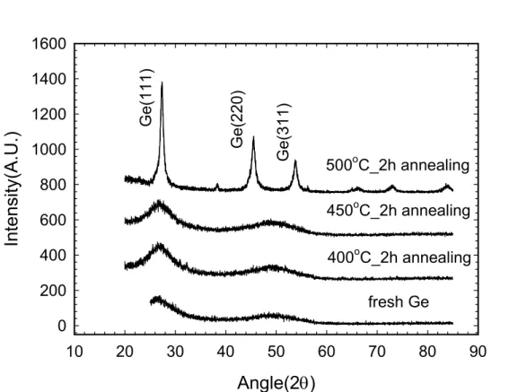
The XRD profiles of the samples annealed at 400 ℃ - 500 ℃ for 2 hours are shown
in Fig. 2-1. We found that the phase of poly-Ge is composed of (111), (220), and (311).
It can be observed that the intensity of the peaks increases with increasing
temperature. Moreover, sharp peaks appear at temperature above 500 ℃, indicating
that the a-Ge film had been transferred into poly-Ge film at temperature of 500 ℃.
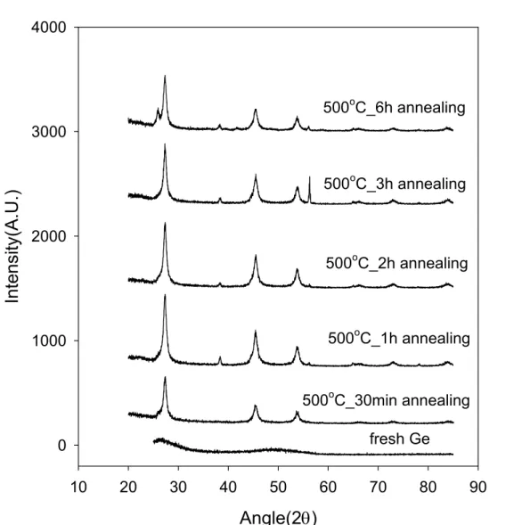
The XRD spectra of the samples annealed at 500 ℃ for times ranging from 0.5 hour
to 6 hours are shown in Fig. 2-2. Obviously, the intensity of the sharp peaks increases
with the annealing duration from 0.5 h to 1 h, and then the intensity almost remains
unchanged with further increase of annealing time. This indicates that the grain of
poly-Ge annealed at 500 ℃ only grows during the initial 1 h and then become
saturated. From the Sherrer relation [29]
θ
λ
cos
d
0.9
L
⋅
×
=
,where L is the grain size, λ is 1.5418 , and d is the full-width half-maximum of the
peak. Based on the relation the grain size of poly-Ge can be estimated by the XRD
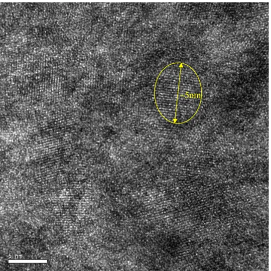
spectra. The TEM images and diffraction pattern of the poly-Ge film annealed at 500
℃ for 1hour are shown in Fig. 2-3(a) and (b), respectively. From the TEM analysis,
the grain size is about 5 nm, and the diffraction pattern shows that the Ge film has
been transformed into poly-Ge, which is in agreement with the XRD profiles. Fig. 2-4
shows the TEM image of Ge film annealed at 500 ℃ for 6hours, and the grain size
estimated by TEM is also about 5 nm. Therefore, it can be inferred that the grain size
increases initially with increasing annealing time, reaches saturation after 1 hour
annealing, and stops growing regardless of the further increase of annealing time
which is consistent with the result from XRD analysis. o
A
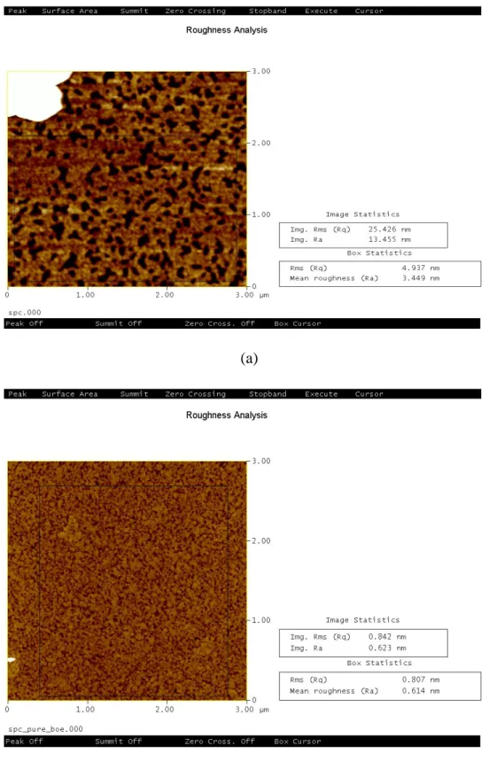
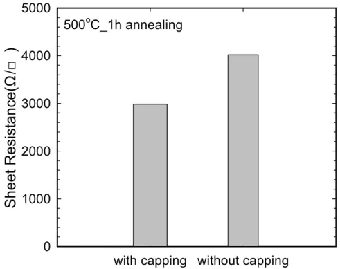
Fig. 2-5 presents the AFM images of poly-Ge film annealed at 500 ℃ for 1 hour,
and the sheet resistance of the samples with and without the capping layer is shown in
Fig. 2-6. Apparently, the surface roughness of the samples without the protection of
capping layer during annealing is larger than that of the oxide capped samples and the
same conclusion can be achieved from the analysis of the sheet resistance. The
rougher surface of the samples without capping layer leads to higher sheet resistance.
As GeO2 will decompose into volatile compound GeO when the annealing 11
temperature is above 430 ℃ [30], it can be inferred that the rough surface is a result
of the decomposition of GeO2. For the samples with oxide capping layer, the
decomposition of GeO2 is suppressed by the capping layer, leading to smoother
surface and lower sheet resistance.
In summary, the suitable annealing time and temperature of SPC for TFTs
fabrication are 1 hour and 500 ℃, and the oxide capping layer is needed when SPC is
carried out.
2-2 The Material Analysis of MIC and MIDA
In this section, we will present the process of sample preparation of MIC and MIDA
first. Then the recrystallization temperature of MIC and the phenomenon of MIDA
will be investigated and discussed.
2-2-1 Sample Preparation of MIC
Initial processes from starting materials to the deposition of a-Ge film were similar
to what had been described in Sec. 2-1-1. After depositing a-Ge film, the wafers were
immediately loaded into the chamber of an electron-beam evaporation system
operated at a base pressure of 5 × 10– 7 Torr. A 5 nm thick Ni film or Al film was
deposited on the a-Ge surface with a rate of 0.3 Ao /s and 5 Ao /s at room temperature, 12
13
respectively. Subsequently, the annealing of the samples was carried out at 250 ℃ -
500 ℃ for 1 h in N2 ambient at atmospheric pressure. The XRD system measured in a
θ-2θ geometry was also used to identify the phase of the annealed samples.
2-2-2 Sample Preparation of MIDA
The processes from preparing starting materials to the deposition of a-Ge film were
the same as the samples of MIC. After depositing the a-Ge film, a TEOS oxide
capping layer was deposited onto the Ge film at 350 ℃ by PECVD system. To
investigate the MIDA technique and the effects of implanted dose, wafers with three
different doping types (undoped, n- and p-type) were characterized where five
implanted doses conditions (5 × 1015 cm-2, 1 × 1015 cm-2, 5 × 1014 cm-2, 8 × 1013 cm-2,
and 3 × 1013 cm-2) of a-Ge samples were prepared by implanting phosphorous (P 31+, at 35 keV) and boron (BF2, at 40 keV) ions for n-type and p-type Ge films, respectively.
The reference/control samples were prepared by annealing the undoped as well as
n-and p- type films with 5 × 1015 cm-2 dosage at 500 ℃ for 1 h in N2 ambience at
atmospheric pressure. After using B.O.E solution to remove the oxide capping layer, a
5 nm thick Ni film was deposited on the a-Ge surface with the process condition
similar to that described in Sec. 2-2-1. Subsequently, the annealing of the testing
14
Unreacted Ni was removed by nitric acid solution for 30 s at room temperature
[31]-[32]. Finally, four-point probe system was used to measure the sheet resistance of
the samples.
2-2-3 Results and Discussion
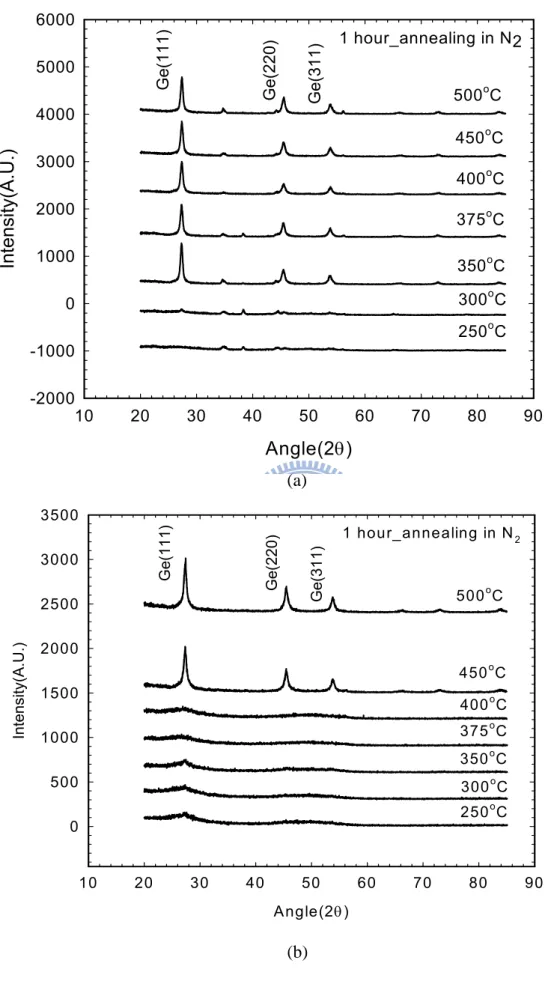
The XRD profiles of Ni MIC and Al MIC are shown in Fig. 2-7. Apparently, it can
be observed that the poly-Ge starts to form at 350 ℃ and 450 ℃ for Ni MIC and Al
MIC, respectively. The difference in crystallization temperature between Ni MIC and
Al MIC is due to the different recrystallization mechanism. For Ni, it will form
germanides with the Ge film at the interface between Ni layer and Ge layer first and
then Ni atoms diffuse into the underlying a-Ge to form a new layer of germanides
leaving poly-Ge behind. By virtue of the low forming temperature of germanides, Ni
tends to have low crystallization temperature. In particular, the temperature needed to
transform a-Ge to poly-Ge can be below 200 ℃, albeit at the expense of annealing
time [5]. For Al, it will also migrate into the a-Ge layer when the temperature is above
the eutectic temperature. The Ge layer remaining behind will transform from a-Ge
into poly-Ge. However, because the eutectic temperature of Al is 423 ℃ [5], [33]
which is higher than the forming temperature of germanides, the crystallization
15
Fig. 2-7. From Fig. 2-7 (a), it can be observed that the peak intensities saturate at
above 350 ℃, and the saturation of intensities indicates that the grains do not grow
when annealing temperature increases because the heterogeneous nuclei formed by
the assistance of Ni suppress the growth of different crystals [5]. In comparison with
the XRD spectra of poly-Ge formed by SPC method where the a-Ge was annealed at
500 ℃ for 1 hour, the peak intensities of Ni-induced crystallization are slightly larger,
meaning that the grain size of poly-Ge film formed by Ni-induced crystallization is
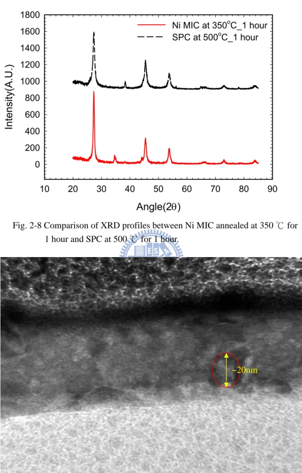
bigger than that of the SPC case as shown in Fig. 2-8. In Fig. 2-9, the TEM image of
Ni-induced crystallization sample annealed at 350 ℃ is presented. From the image,
the grain size of poly-Ge is about 20 nm which agrees with the result of Sherrer
relation and the TEM analysis also agrees with the XRD spectra.
However, because of too many growth collisions and competition of heterogeneous
nuclei [5], the grain size of Ni-induced recrystallized poly-Ge film is still small for
high performance device application even if it is bigger than SPC poly-Ge film.
Hence, MILC which confines the heterogeneous nuclei to a specific location in order
to prevent the collision and competition between heterogeneous nuclei is one way to
enlarge grain size of poly-Ge. Besides, the Ge film remains amorphous even after
annealing at 400 ℃ for 1 hour from the XRD analysis of SPC mentioned in Section
16
as competition between heterogeneous and homogeneous nuclei, further enlarging the
grain size [5].
In addition to lower crystallization temperature, MIC technique can be applied to
activate dopants in Ge at low temperature and compensate for the dopant activation
issues in Ge such as low dopant solid solubility and fast dopant diffusion. This is
because the dopants in Ge, such as phosphorous and boron, will be rearranged into the
substitutional sites and then activated during the MIC process [5]. From the XRD
analysis of Ni MIC mentioned above, boron and phosphorous atoms were activated at
350 ℃ for 1 hour annealing and the control samples were annealed at 500 ℃ for 1
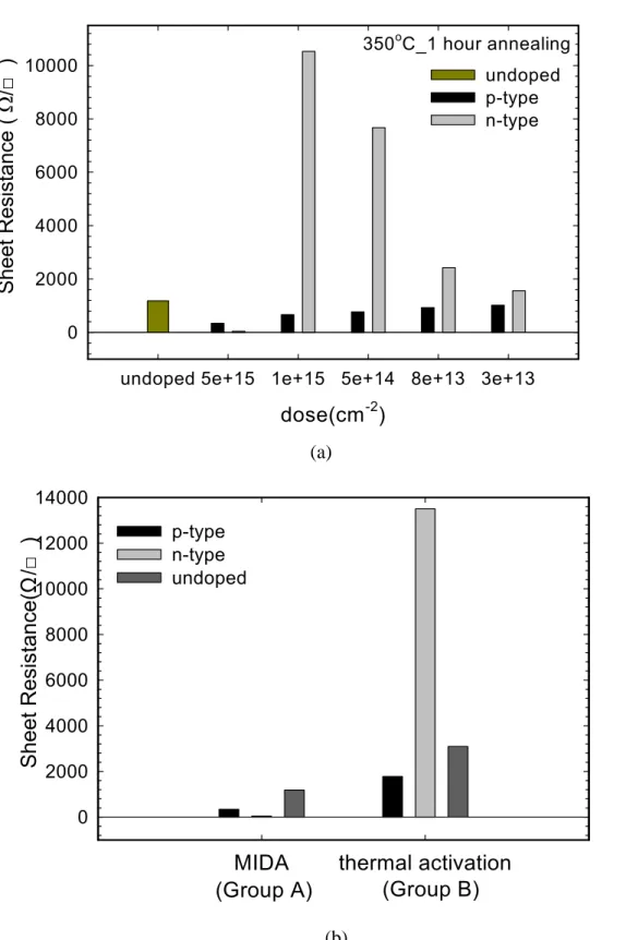
hour. The sheet resistance of MIDA samples with various implanted dose is presented
in Fig. 2-10 (a). Obviously, it can be seen that the lowest sheet resistance for boron
doped samples occurs at the highest implanted dose and it implies that the electrically
activated concentration is the highest at the highest implanted dose. As implanted
dose decreases, the sheet resistance increases and approaches the sheet resistance of
intrinsic samples finally. For phosphorous-doped samples, we observed that the
lowest sheet resistance appeared at a dose of 5 × 1015 cm-2 and the highest one
occurred at a dose of 1 × 1015 cm-2. Ni is speculated to be the culprit for this irregular
resistance-dose dependence because Ni is an acceptor-like metal, and it would trap
17
Ni would be fully filled as the implanted dose rose to a sufficient magnitude and
beyond then there were more non-trapped electrons coming from phosphorous with
further increase of the implanted dose. Therefore, we inferred that the fully-filled
traps donated by Ni resulted in the lowest sheet resistance at a dose of 5 × 1015 cm-2.
The comparison between MIDA samples and thermally activated samples with a dose
of 5 × 1015 cm-2 annealed at 350 ℃ and 500 ℃ for 1 hour, respectively, is shown in
Fig. 2-10 (b). Apparently, it can be seen that the three types (undoped, n- and p-type)
of Ge films in group A are lower than that in group B. For undoped film, the low sheet
resistance would result from the slightly larger grain size and the assistance of Ni
because Ni could slightly reduce the sheet resistance of the film. For doped film, the
high activated concentration led to the low sheet resistance in spite of the fine grain
size of poly-Ge. Hence, it can be seen that the MIDA technique possesses the
advantage of high electrically activated concentration achievable at low annealing
temperature (below 400 ℃) which is suitable for Ge devices and 3D-ICs fabrication.
2-3 The Material Analysis of Germanides
In this section, we present the sample preparation of nickel germanides first. Then
the formation and thermal stability of nickel germanides are also investigated and
2-3-1 Sample Preparation of Germanides
The starting materials were the same as those mentioned above. After standard
cleaning, a 100 nm and a 30 nm thick a-Ge film were deposited on the SiO2 through
sputtering system mentioned in Sec. 2-1-1, respectively. Then, a PECVD system was
used to deposit a TEOS oxide capping layer onto the Ge film at 350 ℃. Next, SPC of
the a-Ge film was performed at 500 ℃ for 1 hour in N2 ambient to form poly-Ge film.
Subsequently, the following processes from removing capping layer to the deposition
of Ni film were the same as what had been mentioned in Sec. 2-2-2 except for the
thickness and deposition rate of Ni film being 30 nm and 2 /s, respectively. Finally, nickel germanides were formed at various temperatures ranging from 250 ℃ to 500
℃ for 30 minutes in N
o
A
2 atmosphere at atmosphere pressure. Nitric acid solution was used to remove the unreacted Ni for 30 s at room temperature.
The systems used to identify the phase and measure the sheet resistance of nickel
germanides were the same as mentioned above, and the surface morphology and the
cross-sectional image were investigated by the AFM and scanning electron
microscopy (SEM), respectively.
2-3-2 Results and Discussion
Fig. 2-11 presents the XRD spectra of the nickel germanides formed on the 100 nm
19
poly-Ge at different annealing temperatures. The peaks at 34.7o, 36.7o, 42.7o, 44.2o,
45.6o, 53.5o are identified as NiGe(111), (120), (021), (211), (121), and (002),
respectively. No peaks correspond to other phases of nickel germanides such as
Ni3Ge2, Ni2Ge, etc. This indicates that poly-NiGe is the only phase at the annealing
temperature ranging from 250 ℃ to 500 ℃. The average grain sizes of poly-NiGe can
be calculated by using the Scherrer relation. From the XRD spectra and the Scherrer
relation, it was observed that the grain size of NiGe gradually increases with
increasing temperature. Fig. 2-12 shows the sheet resistance of the NiGe as a function
of annealing temperature. Clearly, it can be seen that the increase of sheet resistance
occurs at the temperature above 400 ℃. We attribute the phenomenon of the increase
in sheet resistance to the grain growth of poly-Ge. From the previous XRD spectra,
we found that the peak corresponding to the phase of poly-Ge(111) increases and the
full-width half-maximum of the peak narrows at the temperature above 400 ℃, and
this result provides the evidence for grain growth of poly-Ge grain. Further, the
relative intensity of the peaks of the grown poly-Ge(111) were investigated by
magnifying further XRD spectra surrounding the peaks and the average crystallite
size (L) of the Ge was estimated by using the Scherrer relation, as shown in Fig. 2-13.
Obviously, the average grain size (L) of poly-Ge increases with increasing
20
of silicides formed on poly-Si [34]-[35], and it has been ascribed to the fact that the
poly-Si growth beneath the upper silicide film induced the broken silicide film during
annealing. Hence, the growing grain of poly-Si accounts for the drastic increase of the
resistance of the silicide film. It is believed that the silicide film enhances the grain
growth of the poly-Si because of the reduction in grain boundary and interface energy
in the poly-Si. From previous results, we infer that NiGe enhances the grain growth of
the poly-Ge during annealing, especially at the temperature above 400 ℃. As the
grain of poly-Ge is gradually enlarged, the grain penetrates into the upper NiGe film
and the NiGe decomposes. Further, the metal atoms from the decomposed NiGe
diffuse to the poly-Ge/NiGe interface to form new NiGe and then trigger the
formation of the column NiGe. Finally, the NiGe and poly-Ge interlace. The
interlaced grains break the continuous NiGe film and account for the increase of the
sheet resistance [34]-[36].
The surface images of NiGe formed at 300 ℃, 400 ℃, 450 ℃, and 500 ℃ are
shown in Fig. 2-14. From the AFM images, it can be clearly seen that the
phenomenon of growing grain is becoming more and more obvious as the annealing
temperature increases. The same result can be achieved from the SEM images as
shown in Fig. 2-15. Therefore, we believe that the dramatic increase of sheet
21 annealing temperature.
In Fig. 2-16, the XRD analysis of as-deposited sample and nickel germanides
formed on the 30 nm poly-Ge at various annealing temperatures from 250 ℃ to 500
℃ is shown. Unlike the nickel germanides formed on the 100 nm poly-Ge, poly-NiGe
was not the phase formed on the 30 nm poly-Ge anymore and there were no peaks
corresponding to poly-Ge(111) by comparing the XRD spectra of as-deposited sample
and germanides samples which indicated that the poly-Ge was fully consumed. At the
annealing temperature of 250 ℃, Ni2Ge corresponding to the peaks (210), (202), (013)
and (211) at 42.4o, 43.2o, 44.2o, and 44.3o is the only phase formed on the poly-Ge.
However, as the temperature increases, it can be seen that there are two phases of
Ni2Ge and Ni3Ge whose peaks are identified as (111), (200), and (220) at 43.9o, 51.2o,
and 75.3o are simultaneously found in the Ge film at the temperature ranging from
300 ℃ to 400 ℃. Then, while the annealing temperature rises to 450 ℃, Ni3Ge is the
only phase observed in the poly-Ge. Finally, Ni5Ge3 whose peaks are identified as
(002), (403), (203), (602), and (420) at 36.3o, 43.7o, 45.6o, 46.7o, and 47.8o is the only
phase that appears in the Ge film. For 30 minutes annealing, these results indicate that
Ni2Ge is the only phase formed at low temperature and there is a phase competition
between Ni3Ge and Ni2Ge as the temperature increases upon 300 ℃. With increasing
22
Ni2Ge has been fully consumed and Ni3Ge is the only phase found in the poly-Ge at
the temperature of 450 ℃. Ni3Ge would be further consumed to form Ni5Ge3 which is
the only phase observed at 500 ℃. Because Ni5Ge3, Ni2Ge and Ni3Ge are the
transition phase [37]-[42], we believe that the phase of NiGe would be formed as the
annealing time increases to fully consume the transition phase regardless of annealing
temperature. Therefore, for applying to Ge thin film, the thickness of Ni film must be
decreased to the extent that it is fully consumed by Ge or the annealing time must be
long enough to form NiGe which possesses the advantage of low sheet resistance
Chapter 3
Electrical Characteristics of
Poly-Ge TFTs
In this chapter, we describe the fabrication process in detail for five types of
devices first. Subsequently, the measurement setup for electrical characterization is
presented. Finally, we compare and discuss the electrical characteristics of these
devices.
3-1 Process Flow and Device Structures
The cross-sectional view and process flow of devices are illustrated in Figs. 3-1 (a)
~ (e), and Fig. 3-2 ~ Fig. 3-3, respectively. First, 6 inch Si(100) n-type wafers capped
with a 200 nm-thick thermal oxide layer and a 100 nm thick-poly-Si were used as the
starting substrates for fabricating these five types of devices, as shown in Fig. 3-2 (a)
(and Fig. 3-3 (a)). For the devices shown in Fig. 3-1 (a) and (b), after standard
cleaning, a 30 nm thick a-Ge film was deposited on the poly-Si film by ultrahigh
vacuum Ge sputtering system and then the active region was defined by I-line
lithography, followed by etching the a-Ge and poly-Si films, as shown in Fig. 3-2 (b)
(and Fig. 3-3 (b)). Next, a TEOS SiO2 capping layer of 30 nm was deposited by
PECVD at 350 ℃ and SPC was subsequently performed at 500 ℃ for 1 hour in N2
ambient to transform a-Ge to poly-Ge, as shown in Figs. 3-2 (c) and 3-3 (c).
For the device illustrated in Fig. 3-1 (a), which is termed type A, a B.O.E solution
was used to remove the capping layer after poly-Ge film was formed, followed by the
deposition of a 30 nm thick PECVD TEOS SiO2 layer to serve as the gate dielectric.
Afterwards, a 200 nm thick Al film was deposited by electron-beam evaporation
system operated at a base pressure of 5 × 10– 7 Torr with a rate of 5 /s, and was then patterned to serve as the gate electrode (Fig. 3-2 (d)). Boron (BF
o
A
2) S/D implantation was carried out with a dose of 15cm
5 10× -2 at 40 keV with the Al gate electrode serving as the self-aligned implantation mask (Fig. 3-2 (e)). Then, dopant activation
was performed at 400 ℃ for 1 hour at atmosphere, followed by the deposition of a
300 nm thick PECVD TEOS SiO2 layer serving as the passivation layer. Finally, the
devices were completed after using the standard metallization steps to form test pads
(Fig. 3-2 (f)).
For the device shown in Fig. 3-1 (b), termed type B, a lift-off process was used to
confine a 30 nm thick Ni film deposited by electron-beam evaporation system to the
S/D region, followed by performing the annealing at 300 ℃ for 30 minutes to form
25
nickel germanide S/D (Fig. 3-3 (d)). After removing the unreacted Ni by nitric
solution, a B.O.E solution was used to remove the oxide layer and then a 30 nm thick
PECVD TEOS SiO2 layer was deposited to serve as the gate dielectric, followed by
the deposition of a 200 nm thick Al film by electron-beam evaporation system and the
definition of gate electrode (Fig. 3-3 (e)). Eventually, a 300 nm thick PECVD TEOS
SiO2 layer was deposited to serve as the passivation layer and the devices were
completed after using the standard metallization steps to form test pads (Fig. 3-3 (f)).
For the device shown in Fig. 3-1 (c), termed type C, the main difference between
this device and the type A is the raised S/D. I-line lithography was used to pattern the
raised S/D region on the substrates that we had described above and subsequently the
poly-Si film etching was performed. The following fabrication processes from the
deposition of a-Ge film to metallization steps after forming raised S/D region were
similar to what had been described for fabricating the device shown in Fig. 3-1 (a).
For the device shown in Fig. 3-1 (d), termed type D, a 50 nm-thick TEOS SiO2
layer was deposited by low-pressure chemical vapor deposition (LPCVD) on the
poly-Si-capped substrates and then I-line lithography was used to pattern the raised
S/D region, followed by etching SiO2 film with a B.O.E solution. After forming the
raised SiO2 S/D region, the following fabrication processes from the deposition of
26 above.
For the device shown in Fig. 3-1 (e), termed type E, the overall processes were
similar to type A. The main dissimilarity was the absence of poly-Si, and the a-Ge
film was directly deposited onto the thermal oxide layer.
3-2 Measurement Setup for Electrical Characterization
In this section, we will describe the measurement setup before investigating the
electrical characteristics of the devices that we had described in Sec. 3-1. The
Interactive Characterization Software (ICS) software and automated measurement
setup constructed by an AglientTM 4156A semiconductor parameter analyzer are
mainly used to characterize the electrical characteristics of fabricated devices.
Through all measurements, the temperature was kept at room temperature (R.T) by
temperature-regulated hot chuck.
3-3 Fundamental Characteristics of Poly-Ge TFTs
As mentioned in Sec. 2-1-2, the grain size of poly-Ge achieved by SPC method was
very small (about 5 nm) and this result would dramatically affect the device
performance. Some factors including grain size, grain boundaries, interface states,
27
transfer characteristics of devices. With decreasing grain size, grain boundaries and
defects increase and consequently degradation of performance such as smaller drain
current, larger leakage current, mobility and subthreshold swing degradation are
expected as a result. For Ge film, its small band-gap will amplify the effects coming
from the small grain size and further increase the leakage current in comparison with
Si film. The transfer and output characteristics of type A are shown in Fig. 3-4 and the
transfer characteristics of type A and E are compared in Fig. 3-5. We found that type E
did not possess transfer characteristics typical of a well-behaved transistor whereas
type A did. With this result in mind and given the similar processes between these two
devices except for the presence of poly-Si, we inferred that the existence of poly-Si
would increase the crystallinity of poly-Ge film along with increased grain size and
reduced number of grain boundaries and defects. With less defects, the Fermi-level
pinning problem was alleviated and the Al gate electrode could be used to effectively
modulate the potential of channel region, accordingly controlling the switching
behavior of the transistor. XRD was used to investigate the results of SPC which was
carried out in the Ge-on-oxide and Ge-on-poly-Si samples annealed at 500 ℃ for 1
hour, respectively, and the XRD spectra are compared in Fig. 3-6. Obviously, the film
cystallinity of poly-Ge is really better with the presence of poly-Si film and this result
28
Further, type C and D were used to clarify the effects concerning the proper
location of poly-Si. The transfer characteristics of type C are shown in Fig. 3-7 and
the difference in transfer characteristics are compared in Fig. 3-8. Clearly, it can be
seen that the poly-Si film positioned below the Ge S/D has the most apparent effect
on the electrical characteristics of a transistor. We attribute the result to the damage
resulted from the S/D implantation. It is well known that the surface of S/D will be
damaged and transformed into amorphous state from polycrystalline state after
implantation, and the recrystallization will take place in the S/D region during dopant
activation which will result in damage recovery. However, it requires temperature
high enough to provide sufficient energy to fully recover the damage from the
implantation as dopant is activated. Therefore, with the transfer characteristics
observed in Fig. 3-8, we believe that the dopant activation carried out at 400 ℃ for l
hour may not provide enough energy to fully recover damage from implantation and
give rise to many smaller grains and defects in the surface of S/D region. However,
with the assistance of poly-Si, the energy needed to fully recover the damage could be
reduced and consequently the activation temperature of 400 ℃ was sufficient. This
mechanism accounts for the discrepancy in the transfer characteristics.
In Fig. 3-9, the electrical characteristics of type A and C are compared and the drain
29
film was only deposited at the S/D region, poly-Si film was present over the entire
S/D and channel region in type A. Consequently, better crystallinity and therefore
better electrical characteristics are expected in type A. Apparently, we indeed
observed that type A possess better transfer characteristics such as lower threshold
voltage, better subthreshold swing, smaller leakage current, and larger driving current
than type C on account of better crystallinity which causes less grain boundaries and
defects in the poly-Ge film.
For poly-Si TFTs, there are various ways to improve such electrical degradation as
poorer subthreshold swing, larger threshold voltage, and higher leakage current
resulting from the presence of grain boundaries and defects in the poly-Si film,
including plasma treatment in H2/O2 [43], N2/H2 [44], deuterium [45], NH3 [46], or
forming gas annealing with N2/H2 in furnace. This is because the tail and deep states
inside the band-gap will be reduced by these treatments, leading to improved
performance. In a similar fashion, we exploit the forming gas annealing at 400 ℃ for
30 minutes in N2/H2 (5%) atmosphere and NH3 plasma treatment at 300 ℃ for 2
hours with RF power of 300 watts to passivate the dangling bonds at grain boundaries
and interface states at oxide/channel in the poly-Ge film. The transfer and output
characteristics of type A after the plasma treatment are shown in Fig. 3-10 and the
30
Fig. 3-11. Obviously, it can be found that the electrical characteristics of type A is
enhanced in terms of increased driving current and reduced off-state current after the
plasma treatment whereas the subthreshold swing is not apparently improved. From
the result, it indicates that the improvement in on/off ratio mainly comes from
passivating the abundant defects at grain boundaries of S/D region which further
repairs the damage resulting from implantation whereas the passivation of defects and
interface states in the channel region is relative obscure.
Recently, silicide process is widely used to reduce parasitic resistance to enhance
the performance of transistors. Like the silicide process, the germanide process is
expected to alleviate the issue of less dopant solid solubility and further enhance the
performance. In Fig. 3-12, the transfer and output characteristics of type B are
presented. In Fig. 3-13, we compare the transfer characteristics of type A and type B.
Clearly, we observed that the off-state current was suppressed and the on-state current
was increased for type B albeit with worse subthreshold swing. The worse
subthreshold swing of type B might come from the fabrication process such as lift-off
process which resulted in more interface states than type A. The higher on-state
current was what we expected because the sheet resistance of germanide S/D was
lower than implanted S/D and the Schottky barrier height for hole was small [31]-[32],
31
high [31]-[32], [47], ambipolar off-state current typical of metallized S/D device is
strongly suppressed.
In a brief summary for this section, the existence of poly-Si film would enhance the
film crystallinity especially in the recovery of implanted damages at 400 ℃. The use
of germanides and plasma treatment could further improve the electrical
Chapter 4
Conclusions and Future Works
4-1 Conclusions
In this thesis, we studied the material properties and device application of poly-Ge
thin films, and reported five types of devices and material analysis on SPC, MIC,
MIDA poly-Ge, and germanides. From the results of analysis, we found that the grain
size of poly-Ge formed by SPC method saturated at 500 ℃ for 1 hour annealing and
did not increase with increasing annealing time. Hence, annealing at 500 ℃ for 1 hour
is suitable for SPC as required by low temperature process. For further decreasing the
annealing temperature and increasing the grain size, MIC represents an appropriate
approach. With Ni MIC method, annealing at 350 ℃ for 1 hour is enough to
transform a-Ge to poly-Ge because the temperature of forming nickel germanides
which occurs in the initial stage of Ni-induced crystallization is low, and the grain size
is about four times that formed by SPC method. MIDA is an application of MIC. With
Ni-induced crystallization, dopant will be rearranged into the substitutional sites and
consequently the activation temperature can be reduced to 350 ℃ for 1 hour
33
annealing. In order to apply germanide process for the purpose of reducing parasitic
resistance and alleviating the issue of relatively low dopant solid solubility in Ge, the
formation and thermal stability of germanides were investigated. For 100 nm poly-Ge
film, annealing at 300 ℃ to 375 ℃ for 30 minutes was suitable for forming NiGe
with low sheet resistance whereas it might not be appropriate for 30 nm poly-Ge film.
For forming nickel monogermanide in 30 nm poly-Ge film, we found that the
annealing time should be increased to make the transition phase transform into NiGe
or the thickness of Ni film should be decreased to render Ni film fully reacted.
From the transfer characteristics of devices, we inferred that the activation
temperature can not provide enough energy to recover the implanted damage in the
S/D region and results in the degradation of transistor performance. However, we
discovered that the existence of poly-Si film can enhance the film crystallinity
especially in the recovery of implanted damages at 400 ℃ and consequently improves
the transfer characteristics of devices. Finally, through the plasma treatment and the
exploitation of germanide process, the device can be further enhanced.
4-2 Future Works
Devices using poly-Ge film as the channel material have been fabricated and the
34
small grain size formed by SPC method and the implanted damage, the advantages of
Ge film are rarely observed. Hence, there are a lot of works ahead to further enhance
the performance of devices. To improve the performance, some beneficial suggestions
are listed as follows for the future works.
(1) Replace SPC method by using MIC or MILC method to form larger grain size Ge
film. With larger grain size, the performance of devices can be further improved
due to the decrease of grain boundaries and defects.
(2) Decrease the Ni film thickness to the extent that it is fully consumed by Ge or
increase the annealing time in order to form NiGe for 30 nm poly-Ge film. By
using nickel monogermanide as S/D material or using MIDA technique to activate
dopants, device performance is expected to be drastically enhanced, because the
parasitic resistance can be further decreased and the issue of implanted damage is
reduced to a lesser extent
(3) The thickness of poly-Si film may affect the crystallinity of poly-Ge which is
deposited onto the poly-Si film. Hence, by changing the thickness of poly-Si film,
References
[1] E. Gerritsen, N. Emonet, C. Caillat, N. Jourdan, M. Piazza, D. Fraboulet, B. Boeck, A. Berthelot, S. Smith, and P. Mazoyer, “Evolution of Materials Technology for Stacked-Capacitors in 65 nm Embedded-DRAM,” Solid State Electron., vol. 49, pp. 1767-1775, 2005.
[2] K. Saraswat, C. O. Chui, T. Krishnamohan, D. Kim, A. Nayfeh, and A. Pethe, “High performance germanium MOSFETs,” Mater. Sci. Eng. B, vol. 135, no. 3, pp. 242-249, Dec. 2006.
[3] V. Subramanian and K. C. Saraswat, “High-performance germanium-seeded laterally crystallized TFTs forvertical device integration,” IEEE Trans. Electron Devices, vol. 45, no. 9, pp. 1934-1939, Sep. 1998.
[4] J. H. Park, M. Tada, P. Kapur, and K. C. Saraswat, “Low temperature boron and phosphorus activation in amorphous germanium using Ni- and Co-induced crystallization and its application for three-dimensional integrated circuits,” Appl. Phys. Lett., vol. 93, no. 18, p. 183512, Nov. 2008.
[5] J. H. Park, M. Tada, P. Kapur, H. Peng, and K. C. Saraswat, “Self-nucleation free and dimension dependent metal-induced lateral crystallization of amorphous germanium for single crystalline germanium growth on insulating substrate,” J. Appl. Phys., vol. 104, no. 06, p. 064501, Sep. 2008.
[6] S. Zhu and A. Nakajima, “Annealing temperature dependence on nickel-germanium solid-state reaction,” Jpn. J. Appl. Phys., vol. 44, no. 24, pp. L753-L755, Jun. 2005.
36
[7] H. L. Shang, O. S. Harald, K. K. Chan, M. Copel, J. A. Ott, P. M. Kozlowski, S. E. Steen, S. A. Cordes, H. P. Wong, E. C. Jones, and W. E. Haensch, “High mobility p-channel germanium MOSFETs with a thin Ge oxynitride gate dielectric,” IEDM Tech. Dig., pp. 441-444, 2002.
[8] E. P. Gusev, H. Shang, M. Copel, M. Gribelyuk, C. D. Emic, P. Kozlowski, and T. Zabel, “Microstructure and thermal stability of HfO2 gate dielectric deposited on Ge (100),” Appl. Phys. Lett., vol. 85, no. 12, pp. 2334-2336, Sep. 2004.
[9] S. Y. Zhu, R. Li, S. J. Lee, M. F. Li, A. Du, J. Singh, C. X. Zhu, A. Chin, and D. L. Kwong, “Germanium pMOSFETs with Schottky barrier germanide S/D, high-κ gate dielectric and metal gate,” IEEE Electron Device Lett., vol. 26, no. 2, pp. 81-83, Feb. 2005.
[10] C. O. Chui, H. Kim, D. Chi, B. B. Triplett, P. C. Mcintyre, and K. C. Saraswat, “A sub-400 ℃ germanium MOSFET technology with high-κ dielectric and metal gate,” IEDM Tech. Dig., pp. 437-440, 2002.
[11] C. H. Huang, D. S. Yu, A. Chin, C. H. Wu, W. J. Chen, C. Zhu, M. F. Li, B. J. Cho, and D. L. Kwong, “Fully silicided NiSi and germanided NiGe dual gates on SiO2/Si and Al2O3/Ge-on-insulator MOSFETs,” IEDM Tech. Dig., pp. 319-322, 2003.
[12] C. O. Chui and K. C. Saraswat, “Germanium-based technologies: From materials to devices,” Elsevier Science, p. 173, Amsterdam, 2007.
[13] F. A. Trumbore, “Solid solubilities of impurity elements in germanium and silicon,” Bell Syst. Tech. J., vol. 39, no. 1, pp. 205-233, 1960.
37
[14] J. H. Park, D. Kuzum, M. Tada, and K. C. Saraswat, “High performance germanium N+/P and P+/N junction diodes formed at low temperature (≦380 ℃)using metal-induced dopant activation,” Appl. Phys Lett., vol. 93, no. 19, p. 193507, Nov. 2008.
[15] S. Yamaguchi, N. Sugii, and S. K. Park, “Solid-phase crystallization of Si1-XGeX alloy layers,” J. Appl. Phys., vol. 89, no. 4, pp. 2091-2095, Feb. 2001.
[16] H. Watakabe, T. Sameshima, H. Kanno, and M. Miyao, “Electrical properties for poly-Ge films fabricated by pulsed laser annealing,” Thin Solid Films, vol. 508, no. 1-2, pp. 315-317, Jun. 2006.
[17] K. Toko, H. Kanno, A. Kenjo, T. Sadoh, T. Asano, and M. Miyao, “Ni-imprint solid-phase crystallization in Si1-XGeX (X: 0-1) on insulator,” Appl. Phys Lett., vol. 91, no. 4, p. 042111, Jul. 2007.
[18] T. Saito and I. Ohdomari, “Quantitative analysis of the bond rearrangement process during solid phase epitaxy of amorphous silicon,” Philos. Mag. B, vol. 49, no. 5, pp- 471-479, May, 1984.
[19] J. Olivares, A. RodrõÂguez, J. Sangrador, T. RodrõÂguez, C. Ballesteros, and A. Kling, “Solid-phase crystallization of amorphous SiGe films deposited by LPCVD on SiO2 and glass,” Thin Solid Films, vol. 337, no. 1-2, pp. 51-54, Jan. 1999.
[20] C. W. Hwang, M. K. Ryu, K. B. Kim, S. C. Lee, and C. S. Kim, “Solid-phase crystallization of amorphous Si1-XGeX films deposited on SiO2 by molecular beam epitaxy,” J. Appl. Phys., vol. 77, no. 7, pp. 3042-3047, Apr. 1995.
38
[21] K. Toko, I. Nakao, T. Sadoh, T. Noguchi, and M. Miyao, “Electrical properties of poly-Ge on glass substrate grown by two-step solid-phase crystallization,” Int. SiGe Technology and Device Meeting (ISTDM), pp. 30-31, 2008.
[22] T. Sadoh, H. Ohta, and M. Miyao, “Effects of Si layer thickness on solid-phase crystallization of stacked Ge/Si/SiO2 structures,” Jpn. J. Appl.
Phys., vol. 48, no. 3, p. 03B004, Mar. 2009.
[23] T. J. Konno and R. Sinclair, “Metal-contact-induced crystallization of semiconductors,” Mat. Sci. Eng., vol. A179/A180, pp. 426-432, 1994.
[24] F. Katsuki, K. Hanafusa, M. Yonemura, T. Koyama, and M. Doi, “Crystallization of amorphous germanium in an Al/a-Ge bilayer film deposited on a SiO2 substrate,” J. Appl. Phys., vol. 89, no. 8, pp. 4643-4647, Apr. 2001.
[25] A. R. Joshi, T. Krishnamohan, and K. C. Saraswat, “A model for crystal growth during metal induced lateral crystallization of amorphous silicon,” J. Appl. Phys., vol. 93, no. 1, pp. 175-181, Jan. 2003.
[26] W. P. Bai, N. Lu, J. Liu, A. Ramirez, D. L. Kwong, D. Wristers, A. Ritenour, L. Lee, and D. Antoniadis, “Ge MOS characteristics with CVD HfO2 gate dielectrics and TaN gate electrode,” VLSI Symp. Tech. Dig., pp. 121-122, 2003.
[27] N. Wu, Q. Zhang, C. Zhu, D. S. H. Chan, A. Du, N. Balasubramanian, M. F. Li, A. Chin, J. K. O. Sin, and D. L. Kwong, “A TaN-HfO2-Ge pMOSFET with novel SiH4 surface passivation,” IEEE Electron Device Lett., vol. 25, no. 9, pp. 631-633, Sep. 2004.
[28] J. Feng, G. Thareja, M. Kobayashi, S. Chen, A. Poon, Y. Bai, P. B. Griffin, S. S. Wong, Y. Nishi, and J. D. Plummer, “High-performance gate-all-around GeOI
39
p-MOSFETs fabricated by rapid melt growth using plasma nitridation and ALD Al2O3 gate dielectric and self-aligned NiGe contacts,” IEEE Electron
Device Lett., vol. 29, no. 7, pp. 805-807, Jul. 2008.
[29] A. L. Patterson, “The Scherrer formula for X-ray particle size determination,” Phys. Rev., vol. 56, pp. 978-982, November 1939
[30] K. Prabhakaran, F. Maeda, Y. Watanabe, and T. Ogino, “Distinctly different thermal decomposition pathways of ultrathin oxide layer on Ge and Si surfaces,” Appl. Phys Lett., vol. 76, no. 16, pp. 2244-2246, Apr. 2000.
[31] T. Sadoh, H. Kamizuru, A. Kenjo, and M. Miyao, “Low-temperature formation (<500 ℃) of poly-Ge thin-film transistor with NiGe Schottky source/drain,” Appl. Phys. Lett., vol. 89, no. 19, p. 192114, Nov. 2006.
[32] T. Sadoh, H. Kamizuru, A. Kenjo, and M. Miyao, “Ge-channel thin-film transistor with Schottky source/drain fabricated by low-temperature processing,” Jpn. J. Appl. Phys., vol. 46, no. 3B, pp. 1250-1253, Mar. 2007.
[33] S. Gaudet, C. Detaverniar, C. Lavoie, and P. Desjardins, “Reaction of thin Ni films with Ge: phase formation and texture,” J. Appl. Phys., vol. 100, no. 3, p. 034306, Aug. 2006.
[34] S. Nygren, and S. Johansson, “Recrystallization and grain growth phenomena in polycrystalline Si/CoSi2 thin-film couples,” J. Appl. Phys., vol. 68, no. 3, pp. 1050-1058, Aug. 1990.
[35] E. G. Colgan, J. P. Gambino, and B. Cunningham, “Nickel silicide thermal stability on polycrystalline and single crystalline silicon,” Mater. Chem. Phys., vol. 46, no. 2-3, pp. 209-214, 1996.
40
[36] S. L.Hsu, C. H. Chien, M. J. Yang, R. H. Huang, C. C. Leu, S. W. Shen, and T. H. Yang, “Study of thermal stability of nickel monogermanide on single- and polycrystalline germanium substrate,” Appl. Phys. Lett., vol. 86, no. 25, p. 251906, Jun. 2005.
[37] Y. F. Heish, L. J. Chen, E. D. Marshall, and S. S. Lau, “Partial epitaxial growth of Ni2Ge and NiGe on Ge (111),” Thin Solid Films, vol. 162, pp. 287-294, Aug. 1988.
[38] J. Li, Q. Z. Hong, and J. W. Mayer, “Interfacial reaction between a Ni/Ge bilayer and silicon (100),” J. Appl. Phys., vol. 67, no. 5, pp. 2506-2511, Mar. 1990.
[39] J. Ken Patterson, B. J. Park, K. Ritley, H. Z. Xiao, L. H. Allen, and A. Rockett, “Kinetics of Ni/a-Ge bilayer reactions,” Thin Solid Films, vol. 253, no. 1-2, pp. 456-461, Dec. 1994.
[40] L. J. Jin, K. L. Pey, W. K. Choi, E. A. Fitzgerald, D. A. Antoniadis, A. J. Pitera, M. L. Lee, D. Z. Chi, and C. H. Tung, “The interfacial reaction of Ni with (111)Ge, (100)Si0.75Ge0.25 and (100)Si at 400℃,” Thin Solid Films, vol. 462-463, pp. 151-155, Sep. 2004.
[41] F. Nemouchi, D. Mangelinck, J. L. Lábár, M. Putero, C. Bergman, and P. Gas, “A comparative study of nickel silicides and nickel germanides: phase formation and kinetics” Microelectron Eng., vol. 83, no. 11-12, pp. 2101-2106, 2006.
[42] F. Nemouchi, D. Mangelinck, C. Bergman, G. Clugnet, P. Gas, and J. L. Lábár, “Simultaneous growth of Ni5Ge3 and NiGe by reaction of Ni film with Ge,”
41
Appl. Phys. Lett., vol. 89, no. 13, p. 131920, Sep. 2006.
[43] H. N. Chern, C. L. Lee, and T. F. Lei, “The Effects of H2-O2 Plasma Treatment on The Characteristics of Polysilicon Thin Film Transistors,” IEEE Trans. Electron Devices, vol. 40, pp. 2301-2306, 1993.
[44] M. –J. Tsai, F. –S. Wang, K. –L. Cheng, S. –Y. Wang, M. –S. Feng, and H. –C. Cheng, “Characterization of N2/H2 Plasma Passivation Process for Poly-Si Thin Film Transistors (TFTs),” Solid-State Electronics, vol. 38, pp. 1233-1238, 1995.
[45] Y. J. Tung, X. Huang, T. J. King, J. Boyce, and J. Ho, “Improved DC Reliability of Polysilicon Thin-Film Transistors with Deuterium Plasma Treatment,” SID Symp. Dig. of Tech. Papers, vol. 30, pp. 398-401, 1999.
[46] H. –C. Cheng, F. –S. Wang, and C. –Y. Huang, “Effects of NH3 Plasma Passivation on N-Channel Polycrystalline Silicon Thin-Film Transistors,” IEEE Trans. Electron Devices, vol. 44, pp. 64-68, 1997.
Angle(2θ)
10 20 30 40 50 60 70 80 90Intensity(
A.U.)
0 200 400 600 800 1000 1200 1400 1600 fresh Ge 400oC_2h annealing 450oC_2h annealing 500oC_2h annealing Ge(111) Ge(220 ) Ge(311)Fig. 2-1 XRD profiles of SPC samples at various annealing temperatures from 400 ℃ to 500 ℃ for 2 hours. The XRD intensity profile of fresh Ge film is shown as a reference.
Angle(2θ)
10 20 30 40 50 60 70 80 90Inte
nsi
ty(A.U.)
0 1000 2000 3000 4000 fresh Ge 500oC_30min annealing 500oC_1h annealing 500oC_2h annealing 500oC_3h annealing 500oC_6h annealingFig. 2-2 XRD profiles of SPC samples annealed at 500 ℃ for various annealing times from 30 minutes to 6 hours. The XRD intensity profile of fresh Ge film is shown as a reference.
~5nm
(a)
(b)
Fig. 2-3 (a) shows the TEM cross-sectional view of poly-Ge film annealed at 500 ℃ for 1 hour. The circled area in the image indicates the grain size, and (b) presents the diffraction pattern of the poly-Ge film.
~5nm
Fig. 2-4 TEM cross-sectional view of poly-Ge film annealed at 500 ℃ for 6 hours.