國立交通大學
電子工程學系
碩 士 論 文
寬中頻頻寬金氧半混波器設計
Wide-IF-Bandwidth CMOS Mixer Design
研究生:羅斯允
指導教授:胡樹
教授
寬中頻頻寬金氧半混波器設計
Wide-IF-Bandwidth CMOS Mixer Design
研 究 生:羅斯允 Student:Sz-Yun Luo 指導教授:胡樹
Advisor:Robert Hu 國立交通大學 電子工程學系 碩士論文 A ThesisSubmitted to Department of Electronics Engineering & Institute of Electronics College of Electrical and Computer Engineering
National Chiao Tung University in partial Fulfillment of the Requirements
for the Degree of Master
in
Electronics Engineering August 2007
Hsinchu, Taiwan, Republic of China
寬中頻頻寬金氧半混波器設計
學生:羅斯允 指導教授:胡樹
國立交通大學電子工程學系 電子研究所 碩士班
摘要
本篇論文主要描述寬中頻的降頻混波器,並為了,RF 選在 8.7GHz - 17.4GHz,LO 固定在 17.4GHz,IF 則接近 DC-8.7GHz。本設計以 0.18um CMOS 製程,為了不造成系統相當程度的衰落降級,會特別注意對於一些應用在 類比電路,或者是應用在幾 GHz 範圍的設計細節。為了增加訊號轉換的效 益,並且為了減少在 RF 端的電路的共模訊號,以及不要的差模諧波訊號, 在 RF 端電路採用被動式的 Marchand 巴倫。為了降低電路的偏壓,將轉導 對的電流,旁路不經過四個混波的電晶體,並且用 IF 巴倫將輸出的差動訊 號轉換成單端訊號。 相關的電路理論將被發掘,並期望能夠用模擬和量測結果來確認。操 作的更高頻 RF 的類似的混波器,也在計畫實現當中,以利精密的寬中頻接 收模組的研發。
Wide-IF-Bandwidth CMOS Mixer Design
Student: Sz-Yun Luo Advisor: Robert Hu Department of Electronics Engineering & Institute of Electronics
National Chiao Tung University
Abstract
This papers describes the development of a wide-IF-bandwidth down converting mixer, with the RF frequency chosen to be 8.7–17.4GHz, LO fixed at 17.4 GHz and IF close to DC–8.7GHz. The design of this 0.18um CMOS mixer demands particular attention to details, as some techniques developed in the analog and even a few GHz frequency range cannot be directly applied without causing considerable system degradations. To increase the signal transfer efficiency and minimize all the common-mode signals and those unwanted differential mode harmonics at RF circuit, a passive Marchand balun is adopted in designing this mixer's RF circuit. To minimize the circuit's bias voltage Vbias, the drain current of the transconductor pair is set to completely by-pass the four mixing transistors, and IF active balun is applied to convert the output differential signal to single-ended signal.
Related circuit theories will be explored and expect to be confirmed by using both simulated and measured results. Similar mixers that operates at much higher RF frequencies have also been planned, thus facilitate the development of a compact wide-IF-bandwidth receiver module.
誌謝
本論文得以完成,首先要感謝我的指導老師 胡樹
教授,
在碩士班的研究生涯裡,給予我豐富的指導與照顧,不論是研究
上或是平日的生活,都讓我獲得許多的收穫。
感謝匯儀、永旭、天仁、祺源、順意和柏瑋,多謝各位的幫
助和鼓勵,讓我得以順利完成碩士研究。感謝 633 的各位學長、
同學,羽球球友、217 的學弟,以及俊彬、承翰和李明,多謝各位
的陪伴與支持,讓我度過愉快又充實的研究生活。
最後我要感謝我的家人,還有一起長大的夥伴。
Contents
Abstract (in Chinese)………...i
Abstract (in English)……….….ii
Acknowledgement……….iii
Contents………..iv
Figure Captions………...v
Chapter 1 Introduction
1.1 motivation……….1
Chapter 2 Wide-IF-Bandwidth Mixer Design
2.1 Input RF circuit design……….8
2.2 Mixing circuit design……….15
2.3 Output IF circuit design………..17
2.4 Circuit layout and measured results………...19
Chapter 3 Conclusion…………...21
References………..22
Figure Captions
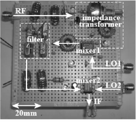
Fig. 1. Photograph of a radio receiver.
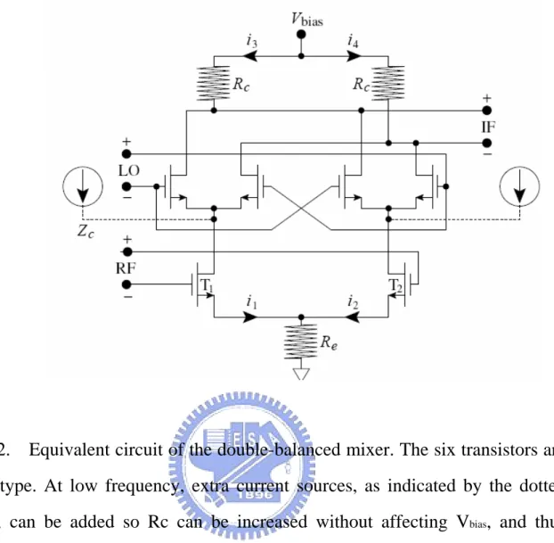
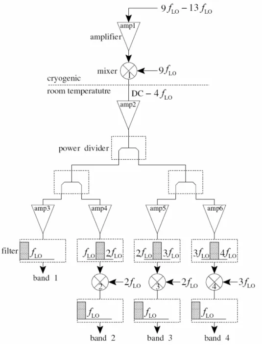
Fig. 2. Equivalent circuit of the double-balanced mixer. Fig. 3. Schematic of the wide-band receiver.
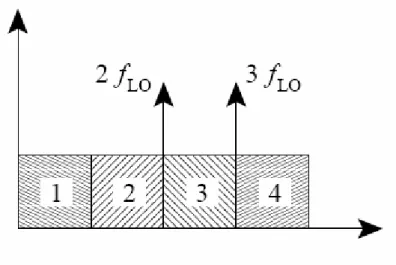
Fig. 4. Distribution of the four IF bands with fLO = 8.7GHz.
Fig. 5. Different circuit configurations used to convert the single-ended RFin
into the differential-mode RFdiff .
Fig. 6. Input RF circuit where the input inductor Ls for impedance match can be implemented as a microstrip line outside the chip. The Marchand balun isused to provide a differential-mode RFdiff.
Fig. 7. Spiral inductor under test.
Fig. 8. Spiral broadside-coupled Marchand coupler. Fig. 9. Mixing circuit with LO injection.
Fig. 10. Output IF circuit.
Chapter 1
Introduction
1.1 Motivation
To transform the radio-frequency (RF) signal to a much lower intermediate frequency (IF), down-converting mixers have to be used. For instance, in the radio receiver shown in Fig. 1, the 7MHz incoming RF can be down-converted to the audio IF via two Philips mixers SA602A, where the local oscillator (LO) frequencies are set to 2.1MHz and 4.9MHz, respectively [1]. To increase the signal transfer efficiency and thus sensitivity, an impedance transformer is then added in front of the first-stage mixer. Because of the relatively narrow band-width, a high-Q (quality factor) band-pass filter is inserted after this mixer. Though an analog circuit stalwart, this transistor mixer's double-balanced circuit configuration have been readily appearing in microwave and millimeter-wave applications; however, not all the techniques developed for further improving the mixer's performance, at low frequency or even a few GHz, are directly applicable at tens of GHz. For example, with large portions of i1 and i2 now come from the extra current sources, as indicated in Fig. 2, both i3 and i4 can be reduced in magnitude [2]. Without affecting the value of Vbias, it is now eligible
using larger Rc to increase the circuit's overall conversion gain. However, since the extra current sources are usually made of p-type transistors, their output impedance Zc tends to be small at high frequency, and thus deteriorates this mixer's performance as frequency increases. If the p-type transistor is replaced by a large resistors for constant Zc, the bias voltage Vbias needs to be increased
for this part of circuit [3].
mixer is even obvious when considering another factor: IF bandwidth. So far, most of the mixers with normal-biased transistors, as contrast to resistive transistors with no drain bias, have their wide-band proclamation illustrated by shifting the LO across the intended RF bandwidth, while keeping the IF band-width comparatively small [4], i.e., wide RF-bandwidth but narrow IF-bandwidth. With an IF bandwidth of hundreds of MHz, a large output can be easily achieved by replacing each Rc in Fig. 2 with an appropriate p-type transistor, as which is capable of providing a large impedance at low frequency. However, when the IF bandwidth is extended to several GHz, the rapidly decreasing impedance of this active p-type load becomes a liability, as it leads to a large variation of the conversion gain over the intended bandwidth: extremely high at the low-end of the output frequency range while at high-end it is mediocre or no better than that of mixers using Rc. Likewise, the use of extra current source and large Rc for 10.20dB conversion gain will lose its appeals as IF bandwidth increases, because the IF voltage is now mainly determined by the much lower input impedance of the following stage rather than Rc itself.
Fig 3 is the schematic of a millimeter-wave receiver which will be used in the form of array for the determination of the anisotropy of the cosmic microwave background radiation, and it demands the employment of several wide IF bandwidth mixers. As indicated by the number inside the crossed circle, the first mixer will down-convert the amplified 78.3 - 113.1GHz signal to DC - 34.8GHz, or more precisely, 0.2 - 34.8GHz. Four bands are then separated using amplifiers, filters and another three mixers, with each has the same IF bandwidth of 8.7GHz; the LO frequencies are fixed at 17.6GHz, 17.6GHz and 26.3GHz for equal bandwidth partition. Though the commercial Marki M1R0920, Hittite HMC292 and HMC329 can be used for mixers 2, 3 and 4, respectively, their conversion
losses require the adjacent amplifiers inside and outside module to be very high-gain. Besides, these passive mixers' poor impedance matching at RF, LO and IF ports inevitably contribute to the rippled responses versus frequency in their corresponding bands.
The existing system's shortcomings therefore prompt us to design the wide IF-bandwidth down-converting mixers with matched ports, low noise temperature, positive over-all conversion gain and, most important of all, a clear IF output spectrum. In this paper, we intend to focus on the second mixer, which has its input frequency range being 8.7 - 17.4GHz and LO set to 17.4GHz, as shown in Fig. 4. The reason why not using a 8.7GHz LO to down-convert the RF is because this LO is bordering the IF band, thus any residual LO at IF output is hard to remove; by contrast, a 17.4GHz LO will not have this problem.
Fig. 1. Photograph of a radio receiver. The mixers are Philips SA602A. The impedance transformer comprises inductor, varactor, potentiometer, toroid transformer and capacitors. The band-pass filter inside the dotted box is made of quartz-crystal resonators and ceramic capacitors. LO1 is 2.1MHz and LO2 is 4.9GHz.
Fig. 2. Equivalent circuit of the double-balanced mixer. The six transistors are of n-type. At low frequency, extra current sources, as indicated by the dotted lines, can be added so Rc can be increased without affecting Vbias, and thus
Fig. 3. Schematic of the wide-band receiver. With fLO = 8.7GHz, the incoming
78.3 - 113.1GHz signal will first be amplified and then down converted onto DC.34.8GHz, which will be further split into four separate bands of equal bandwidth. The front-end amplifier and mixer are located inside the cryostat from sensitivity consideration, while the rest are at room temperature.
Fig. 4. Distribution of the four IF bands with fLO = 8.7GHz. The DC - 4fLO
frequency range will be divided into 4 bands. The first band can be extracted using a low-pass filter while the second, third and forth bands have to be down-converted first using mixers with their LO frequency set to 2fLO, 2fLO and
Chapter 2
Wide-IF-Bandwidth Mixer Design
2.1 Input RF circuit design
The commercial TSMC 0.18um RF-CMOS processing technology is chosen in designing this mixer. To facilitate the circuit analysis, we intend to have all the transistors used in this mixer to be identical. In this section, the mixer's input RF circuit will be explored.
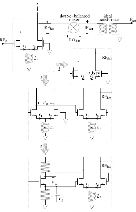
Granted, there are many circuit configurations available for converting the single-ended RF signal to differential-mode, and one is the differential pair with one input port grounded, as shown in Fig. 5. If two RF signals, say, 11GHz and 9GHz, are presented at the input, then both differential-mode and common-mode 11GHz and 9GHz will be appearing at the transistors' gates. Due to the inevitable nonlinearity of the transistors, both 2GHz (as 11GHz minus 9GHz) and 20GHz (as 11GHz plus 9GHz) differential-mode signals can be detected at RFdiff , as defined on the drains. Now, even with a perfect
differential-mode LO of 8.7GHz and an ideal IF transformer, there will be the 6.7GHz (as 8.7GHz minus 2GHz) and 11.3GHz (as 20GHz minus 8.7GHz) signals at IFout. With our designated DC.8.7GHz IF bandwidth, this unintended
6.7GHz thus causes spectrum disturbance.
Of course, it is possible replacing one n-type transistor with an appropriate p-type one, so the biasing current i2 can be reversed and equals in magnitude to
i1, as indicated by the arrow 1 of Fig. 5. With Ls readily removed, the
common-mode signal on RFdiff can be suppressed. Indeed, it works excellent
with several-GHz RF and narrow-band IF [5], though a larger Vbias will be
impedance between the transistor's emitter and ground can no longer be neglected at high frequency, the 9GHz and 11GHz signals at RFin still bring in
the differential-mode 2GHz and 20GHz ones at RFdiff , and thus 6.7GHz and
11.3GHz output at IFout.
Rather than using the p-type transistor, if another differential pair is added to the original circuit configuration, as now indicated by arrow 2 of Fig. 5, the unwanted 6.7GHz will still appear at IFdiff by the same reasoning. Lastly,
conversion gain degradation notwithstanding, differential-mode signal can also be extracted from the drain and source of the transistor, as indicated by arrow 3 of Fig. 5, where the capacitor Cp is for high-frequency phase compensation.
With good common-mode suppression for the fundamental frequencies, the 9GHz and 11GHz on Vα will mostly be differential-mode; however, the 2GHz
and 20GHz signals (due to the nonlinearity of the first transistor) at Vα are
mostly common-mode. When the nonlinearity of the differential-pair transistors comes to play, differential-mode 7GHz (9GHz minus 2GHz), 9GHz (20GHz minus 11GHz), 13GHz (9GHz plus 2GHz), and 31GHz (20GHz plus 11GHz) signals all appear at RFdiff .
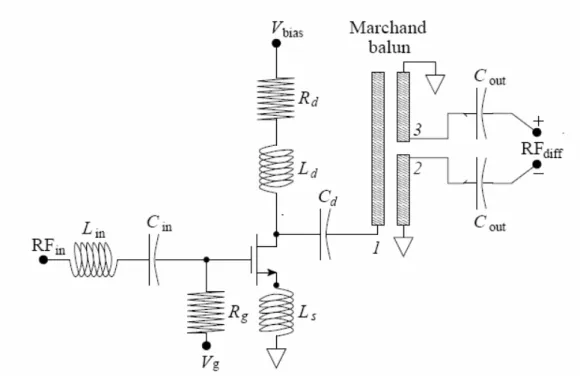
To minimize all the common-mode signals and those unwanted differential -mode harmonics at RFdiff , a passive Marchand balun is adopted in designing
this mixer's RF circuit [7], as shown in Fig. 6. Neglecting its loss, this balun can have its S-parameters expressed as
the number in the figure, is matched, while the output signals on ports 2 and 3 are 180 degrees out of phase [8]. As the balun will indeed be fabricated on the lossy silicon substrate, this RF front-end loss will greatly affecting this mixer's noise performance, a one-stage transistor circuit is then constructed in front of this balun for noise suppression. A matched input impedance of this input RF circuit can now be achieved by fine-tuning the transistor's loading impedance and its input inductor Ls [6]. At this moment, the input RF circuit can have its S11 below -15dB within the intended frequency range. As this part of the mixer operates at 8.7 - 17.4GHz, which is far beyond the reach of the active load from p-type transistors, a series Rd Ld is chosen for the transistor's drain bias branch, whereas the gate bias is through a large resistor. Of course, with relaxed constrain on chip size, transformer feedback can indeed be applied for achieving even better S11 while retaining a low noise temperature [9]. As for the bisymmetric class-AB input stage [10], [11], the resistive version tends to be noisy while the inductive version takes too much space. Besides, the nature of the RF signal in our system means it is far from high power.
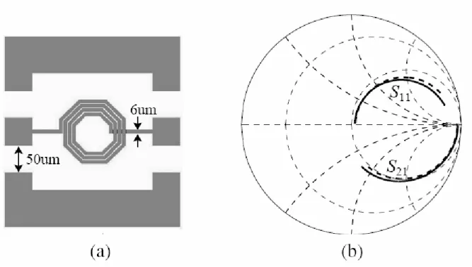
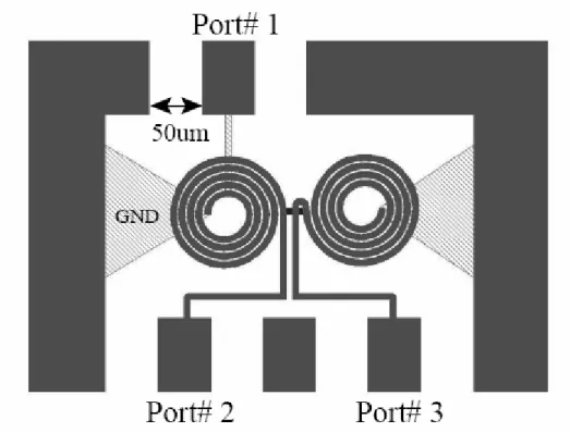
Prior to the design of the Marchand balun, accuracy of the simulation needs to be confirmed. Fig. 7 shows both the measured and simulated results of a 3.5-turn spiral inductor. Here the solid curve is provided by the vendor, while the dashed curve is carried out by us using HP-Momentum, with 10Ω-cm resistance chosen for the lossy silicon substrate, and the top-layer metal is 6um-wide. Agreements between the measured and simulated results remove any suspicious on the simu- lation accuracy. Fig. 8 is the layout of the spiral broadside-coupled Marchand balun, with input port 1 and output ports 2 and 3 indicated. The simulated output phase difference is 180±3 degrees, and which can be further improved.
Fig. 5. Different circuit configurations used to convert the single-ended RFin
into the differential-mode RFdiff . Perfect differential-mode LO and idea IF balun
Fig. 6. Input RF circuit where the input inductor Ls for impedance match can be implemented as a microstrip line outside the chip. The Marchand balun is used to provide a differential-mode RFdiff.
Fig. 7. Spiral inductor under test. (a) This 3.5-turn spiral inductor has its line width set to 6um, the inner radius 31um and the line separation 2um. The input and output pads are 50x50um2. (6) On the Smith chart, the solid lines are the S11 and S21 from 0.1 - 20GHz measured by the vendor; the dashed lines are the simulated counterparts where the each pad's capacitance has been de-embedded.
Fig. 8. Spiral broadside-coupled Marchand coupler. Port# 1 is the input, and ports# 2 and 3 are the output with 180-degree phase difference.
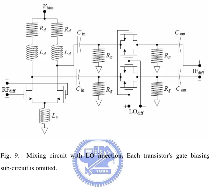
2.2 Mixing circuit design
To minimize the circuit's bias voltage Vbias, the drain current of the differential
pair is set to completely by-pass the four mixing transistors, as shown in Fig. 9. And by operating these four mixing transistors as variable resistors where the resistance is modulated by the LO signal, the biasing circuit can be greatly simplified as both the drain and source of the transistors are now connected to ground through large resistors. One plausible advantage of this resistive mixer is that it will have small second-order intermodulation [12], though a detailed analysis on the CMOS situation has not been carried out yet. The other advantage is that the equivalent circuit for each of these mixing transistors will now be less frequency-dependency, thus is more suitable for wide IF bandwidth application. In the simulation, a larger conversion gain can indeed be observed when the drain bias is applied; however, discernible conversion gain variation over the whole IF bandwidth restrains its usefulness. Resistive mixer, on the other hand, tends to have constant conversion gain, and is more straightforward in terms of biasing. Since the analysis of the mixers is mostly limited to narrow IF bandwidth [13], its wideband counterpart needs to be theorized too in our case, which means this part of the circuit is far from finished.
Fig. 9. Mixing circuit with LO injection. Each transistor's gate biasing sub-circuit is omitted.
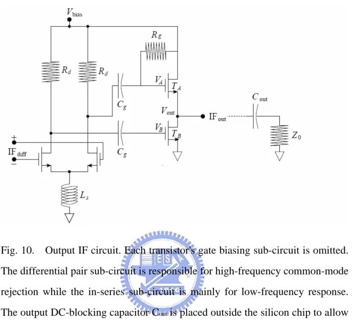
2.3 Output IF circuit design
Even being designated as IF, its 8.7GHz upper frequency prohibits the use of p-type transistors and thus some related circuit techniques for converting the differential-mode IF to single-end signal, as which will cause a large conversion gain degradation when frequency increases. On the other hand, the 0.2GHz lower frequency of the IF band prohibits the use of on-chip passive baluns. Active balun made of two n-type transistors is therefore employed, as shown in Fig. 10. Neglecting Cgs and Cgd, there is at very low frequency
where Z0 L is the in-parallel impedance of Z0, RAds and RBds, and the superscript
indicates the transistor designated. In addition to improving the output linearity, the optional emitter resistors (not shown in the schematic) can even adjust each transistor's transconductance gain if they are not equal to each other [14], [15]. To improve the common-mode rejection ratio at high frequency, a conventional differential pair is further added, with it emitter inductor Ls resonates at 10GHz. A common-mode rejection ration (CMRR) around 40dB is observed across the whole bandwidth.
Fig. 10. Output IF circuit. Each transistor's gate biasing sub-circuit is omitted. The differential pair sub-circuit is responsible for high-frequency common-mode rejection while the in-series sub-circuit is mainly for low-frequency response. The output DC-blocking capacitor Cout is placed outside the silicon chip to allow
2.4 Circuit layout and measured results
As shown in Fig. 11, a simplified mixer circuit has been designed and submitted for fabrication for a preliminary evaluation. However, due to some inadvertent layout errors, this circuit cannot function properly and no measured results are obtained.
Fig. 11. Layout of the preliminary wideband mixer. Due to some layout errors, no measured results can be obtained from this circuit.
Chapter 3
Conclusion
With the design of the wide IF bandwidth mixer using 0.18um CMOS technology in progress, we expect a reliable prototypical circuit to be available in two year's time. Then the 0.13um CMOS technology will be adopted in designing all the three mixers mentioned at the beginning of this paper, which together cover the RF frequency of 8.7.34.8GHz. Meanwhile, theory for the optimized impedance of the input Marchand balun will be explored and theorized, so does the intended bias for the four mixing transistors. As for LO balun, since it works at one frequency point for each mixer, we are looking for ways to minimize its physical dimension by further folding its layout.
References
[1] D. B. Rutledge, The Electronics of Radio, ISBN 0521646456, Cambridge University Press, 1999.
[2] L. A. MacEachern, T. Manku, “A charge-injection method for Gilbert cell biasing,” IEEE Canadian Conference on Electrical and Computer Engineering, vol. 1, pp. 365-367, May 1998.
[3] M. L. Schmatz, U. Lott, W. Baumberger, W. Baechtold, “Novel design topology for ultra low power down converters with broadband ob chip matching network,” IEEE Trans. Microwave Theory Techniques, vol. 43, no. 12, pp. 2946-2951, Dec. 1995.
[4] S. J. Mahon, et. al, “Broadband integrated millimeter-wave up- and down-converter GaAs MMICs,” IEEE Trans. Microwave Theory
Techniques, vol. 54, no. 5, pp. 2050-2060, May 2006.
[5] T. T. Hsu, C. N. Kuo, “Low power 8-GHz ultra-wideband active balun,”
IEEE 2006 Topical Meeting on Silicon Monolithic Integrated Circuits in RF systems, pp. 365-368, Jan. 2006.
[6] R. Hu, “Wide-band matched LNA design using transistor's intrinsic gate-drain capacitance,” IEEE Trans. Microwave Theory Techniques, vol. 54, no. 3, pp. 1277-1286, March 2006.
[7] N. Marchand, “Transmission-line conversion transformers,” Electronics, vol. 17, no. 12, pp. 142-145, Dec. 1944.
[8] K. S. Ang, I. D. Robertson “Analysis and design of impedance-transforming planar Marchand baluns,” IEEE Trans. Microwave Theory Techniques, vol. 49, no. 2, pp. 402-406, Feb. 2001.
broadband matching,” 2006 IEEE Radio Frequency Integrated Circuits
Symposium, pp. 53-56, June. 2006.
[10] B. Gilbert, “The MICROMIXER: a highly linear variant of the Gilbert mixer using a bisymmetric class-AB input stage,” IEEE J. Solid-State
Circuits, vol. 32, pp. 1412-1423, Sep. 1997.
[11] S. C. Tseng, C. C. Meng, C. H. Chang, C. K. Wu, G. W.Huang, “Monolithic broadband Gilbert micromixer with an integrated Marchand balun using standard silicon IC process,” IEEE Trans. Microwave Theory Techniques, vol. 54, no. 12, pp. 4362-4371, Dec. 2006.
[12] S. A. Maas, “A GaAs MESFET mixer with very low intermodulation,”
IEEE Trans. Microwave Theory Techniques, vol. mtt-35, no. 4, pp. 425-
429, Apr. 1987.
[13] R. A. Pucel, D. Masse, “Performance of GaAs MESFET mixers at X band,”
IEEE Trans. Microwave Theory Techniques, vol. mtt-24, no. 6, pp.
351-360, June 1976.
[14] H. Ma, S. J. Fang, F. Lin, K. S. Tan, “A high performance GaAs MMIC up-converter with an automatic gain control amplifier,” 19th Annual
Gallium Arsenide Integrated Circuit Symposium, pp. 232-235, Oct. 1997.
[15] R. H. Lee, et. al., “Circuit techniques to improve the linearity of an up-conversion double balanced mixer with an active balun,” 2005 Asia
Vita
姓名:羅斯允
學歷:私立元智大學電機工程學系 (88年9月~93年6月) 國立交通大學電子研究所固態組 (93年9月~96年8月)
論文題目:寬中頻頻寬金氧半混波器設計