氨氣電漿處理對複晶矽薄膜電晶體之電特性影響探討
105
0
0
全文
(2) 氨氣電漿處理對複晶矽薄膜電晶體之電特性影響探討 研究生: 劉俊彥. 指導教授: 葉清發 博士 國立交通大學. 電子工程學系. 電子研究所碩士班. 摘要 利用複晶矽薄膜電晶體(poly-Si TFTs)製作畫素元件及週邊驅動電路並 將它積體化於大面積玻璃基板已成為未來製造主動式矩陣液晶顯示器的趨勢。目 前複晶矽薄膜電晶體的異常漏電流是一個待解決且刻不容緩的議題。在本論文 中,我們使用氮化矽(Si3N4)當作底部閘極之絕緣層,探討經氨氣電漿處理後氫原 子與氮原子能夠累積在電晶體的通道內之效應,如此可進一步在汲極接面中填補 通道的缺陷數量,可更有效降低元件漏電流之情形。除此之外,我們利用表面電 位顯微鏡(KFM)來描述經氨氣電漿處理前後汲極接面能帶圖的變化情形,且此與複 晶矽電晶體的異常漏電流有關聯。另一方面,我們也探討了長時間作氨氣電漿處 理後,對複晶矽薄膜電晶體電特性之影響。對離子而言要穿透氮化矽薄膜是困難 的。因此,此效應造成使用氮化矽與二氧化矽作為複晶矽電晶體的閘極絕緣層之 不同行為。. i.
(3) Investigations of NH3 Plasma Treatment on the Electrical Characteristics of Poly-Si Thin Film Transistors Student: Chun-Yen Liu. Advisor: Dr. Ching-Fa Yeh. Institute of Electronics National Chiao Tung University. Abstract Utilizing polycrystalline silicon thin-film transistors (poly-Si TFTs) as pixel switching elements and peripheral driver circuits is the future trend for manufacturing active-matrix liquid-crystal displays (AMLCDs). Currently, the anomalous leakage current of poly-Si TFTs is an important issue. In this thesis, we used Si3N4 as the insulator of bottom-gated TFTs to investigate the effects of nitrogen and hydrogen radicals accumulated within the channel by NH3 plasma treatment. A reduction of the leakage current was observed because of effectively defect reduction in the drain junction. Furthermore, variations of the profiles of energy band in the drain junction before and after NH3 plasma treatment are characterized by Kelvin Probe Force Microscope (KFM), and are used to associate with the anomalous leakage current of poly-Si TFTs. On the other hand, the influence of long-time NH3 plasma treatment on the electrical characteristics of poly-Si TFTs is studied. It is hard for atomic ions to penetrate into the Si3N4 layer. Therefore, the effect results in the different behaviors of poly-Si TFTs with Si3N4 and SiO2 as the gate insulators.. ii.
(4) Acknowledgment 首先,我要感謝我的指導教授葉清發博士,由於教授在我這兩年碩士研究過 程中的細心指導,使我能順利完成我的學業,謝謝老師。另尤其也要感謝陳添富 學長與羅正忠老師,在葉教授借調日本期間中給予我在實驗上的一些建議與幫助。 其次,我要感謝交大電子所這兩年來的栽培,系所老師們的認真教學使身為 學生的我終身受用不盡。另外,我要感謝國家奈米實驗中心(NDL)的研究員及設 備工程師們,由於你們的協助使我能在一流的製程設備中從事我的研究工作。 感謝 Yeh's groups 中蕭智文、王碩晟、謝志民學長們的指導與協助。感謝 薛國欽、林榮祥、林余俊、張志廉、張志揚、鍾文俊、蘇柏智等同學在實驗過程 中的互相鼓勵及協助,我想大家一定會懷念那段一起唸書與作實驗時光。此外, 也要感謝蔣陳偉學弟們熱心協助,謝謝。 最後,我要感謝我的父母親-劉正德先生與范惠珠女士以及姊夫高銘和、郭 洪斌先生,姊姊劉稚文、劉凱文,妹妹劉照文,女朋友陳昱如小姐在我求學及從 事研究過程中給我的最大的支持與關心,使我能在兩年的時光中順利完成我的學 業,謝謝你們。. iii.
(5) Contents Chinese Abstract. •••••••••••••••••••••••••••••••••••••••••••••••••••••••••••••••••••••. i. English Abstract. •••••••••••••••••••••••••••••••••••••••••••••••••••••••••••••••••••••. ii. Acknowledgment. •••••••••••••••••••••••••••••••••••••••••••••••••••••••••••••••••••••. iii. Contents. •••••••••••••••••••••••••••••••••••••••••••••••••••••••••••••••••••••. iv. Table Captions. •••••••••••••••••••••••••••••••••••••••••••••••••••••••••••••••••••••. vi. Figure Captions. •••••••••••••••••••••••••••••••••••••••••••••••••••••••••••••••••••••. vii. Chapter 1 Introduction 1.1 General Background and Motivation 1.2 Organization of Thesis. •••••••••••••••••••••••••••••••••••••• 1. •••••••••••••••••••••••••••••••••••••••••••••••••••••••. 4. Chapter 2 Investigatios of Defect Passivation in the Drain Junction on the Leakage Current of Poly-Si TFTs 2.1 Introduction. ••••••••••••••••••••••••••••••••••••••••••••••••••••••••••••••••••••• 6. 2.2 Experiment Details 2.2.1 Fabrication of bottom-gated P-type poly-Si TFTs using SPC crystallization ••8 2.2.2 Sample for ESCA/SIMS analysis. ••••••••••••••••••••••••••••••••••••••••••• 11. 2.2.3 Sample for Kelvin Probe Force Microscope (KFM) analysis. ••••••••••• 13. 2.3 Results and Discussions 2.3.1 Physical mechanism on the leakage current. •••••••••••••••••••••••••••••• 14. 2.3.2 Hydrogenation effect on high VDS leakage current and physical property analysis. ••••••••••••••••••••••••••••••••••••••••••••••••••••••••••••••••••••••. 16. 2.3.3 Hydrogenation effect on low VDS leakage current and physical property analysis. 2.4 Summary. •••••••••••••••••••••••••••••••••••••••••••••••••••••••••••••••••••••• •••••••••••••••••••••••••••••••••••••••••••••••••••••••••••••••••••••••••. iv. 19 21.
(6) Table Captions Table 2.1 The electrical characteristics of bottom-gated poly-Si TFTs before and after NH3 plasma hydrogenation. Table 2.2 The electrical characteristics of p-type top-gated poly-Si TFTs using SPC/ELA techniques before and after NH3 plasma hydrogenation. Table 2.3 The electrical characteristics of n-type top-gated poly-Si TFTs using SPC/ELA techniques before and after NH3 plasma hydrogenation.. vi.
(7) Figure Captions Chapter 1 Figure 1.1 The equivalent circuit diagrams of the pixel and its layout in AMLCDs.. Chapter 2 Figure 2.1 Key process flows of p-type bottom-gated poly-Si TFTs. Figure 2.2 Key process flows of SIMS/ESCA samples. Figure 2.3 Key process flows of KFM samples. Figure 2.4 Schematic illustration of the leakage current model in poly-Si TFT. Figure 2.5 (a) Transfer characteristics for comparison of p-type bottom-gated TFTs using SPC/ELA before and after hydrogenation at VDS= -0.1 V. Sample A (gate oxide), B (gate nitride) treat 360 min, and 300min NH3 plasma passivation, respectively. Figure 2.5 (b) Transfer characteristics for comparison of p-type bottom-gated TFTs using SPC/ELA before and after hydrogenation at VDS= -5 V. Sample A (gate oxide), B (gate nitride) treat 360 min, and 300min NH3 plasma passivation, respectively. Figure 2.6 (a) Transfer characteristics for comparison of p-type top-gated TFTs using SPC/ELA before and after hydrogenation at VDS= -0.1 V. Both of SPC (gate oxide) and ELA (gate oxide) samples treat 300min NH3 plasma passivation. Figure 2.6 (b) Transfer characteristics for comparison of p-type top-gated TFTs using SPC/ELA before and after hydrogenation at VDS= -5 V. Both of SPC (gate oxide) and ELA (gate oxide) samples treat 300min NH3 plasma passivation. Figure 2.7 (a) Transfer characteristics for comparison of n-type top-gated TFTs before and after hydrogenation at VDS= 0.1 V. SPC and ELA samples treat 300 min, and 360 min NH3 plasma passivation, respectively. Figure 2.7 (b) Transfer characteristics for comparison of n-type top-gated TFTs before vii.
(8) and after hydrogenation at VDS= 5 V. SPC and ELA samples treat 300 min, and 360 min NH3 plasma passivation, respectively. Figure 2.8 (a) The SIMS profiles of SiN for sample C (gate dielectric: SiO2) and D (gate dielectric: Si3N4) with 240 min, and 480 min NH3 plasma treatment. Figure 2.8 (b) The SIMS profiles of hydrogen concentration for sample C (SiO2) and D (Si3N4) with 240 min, and 480 min NH3 plasma treatment. Figure 2.8 (c) The SIMS profiles of oxygen concentration for sample C (SiO2) and D (Si3N4) before and after 240 min, and 480 min NH3 plasma treatment. Figure 2.9 (a) The ESCA (XPS) profiles of silicon binding energy for sample C (SiO2) before and after 120 min, and 480 min NH3 plasma treatment. Figure 2.9 (b) The ESCA (XPS) profiles of silicon binding energy for sample D (Si3N4) before and after 120 min, and 480 min NH3 plasma treatment. Figure 2.10 (a) The variation of surface potential for sample E (P+/i junction) before NH3 plasma treatment was measured by KFM. Figure 2.10 (b) The variation of surface potential for sample E (P+/i junction) before NH3 plasma treatment of 6 h was measured by KFM. Figure 2.11 Schematic illustrations of defect-reduction in the drain junction.. Chapter 3 Figure 3.1 Possible pathways for hydrogen migration from a gaseous source to the active channel region of a top-gated poly-Si TFT structure. Figure 3.2 Key process flows of the bottom-gated poly-Si TFTs using SPC processes. Figure 3.3 Key process flows of the top-gated poly-Si TFTs using SPC/ELA processes. Figure 3.4 Subthreshold Swing determined at VDS= -0.1V as function of NH3 plasma passivation time for W= 10µm and L= 2 µm p-type bottom-gated poly-TFTs Figure 3.5 (a) Threshold voltage determined at VDS= -0.1V as function of NH3 plasma passivation time for W= 20µm and L= 5 µm p-type bottom-gated poly-TFTs. Figure 3.5 (b) Threshold voltage determined at VDS= -0.1V as function of NH3 plasma viii.
(9) passivation time for W= 20µm and L= 5 µm p-type top-gated poly-TFTs. Figure 3.5 (c) Threshold voltage determined at VDS= -0.1V as function of NH3 plasma passivation time for W= 20µm and L= 10µm n-type poly-TFTs. Figure 3.6 (a) Mobility determined at VDS= -0.1V as function of NH3 plasma passivation time for W= 10µm and L= 2 µm p-type bottom-gated poly-TFTs. Figure 3.6 (b) Mobility determined at VDS= -0.1V as function of NH3 plasma passivation time for W= 20µm and L= 10 µm p-type top-gated poly-TFTs. Figure 3.6 (c) Mobility determined at VDS= 0.1V as function of NH3 plasma passivation time for W= 20µm and L= 5 µm n-type poly-TFTs. Figure 3.7 (a) The leakage currrent determined at VDS= -5V as function of NH3 plasma passivation time for W= 10µm and L= 2 µm p-type bottom-gated poly-TFTs. Figure 3.7 (b) The leakage currrent determined at VDS= -5V as function of NH3 plasma passivation time for W= 20µm and L= 10 µm p-type top-gated poly-TFTs. Figure 3.8 (a) Effective trap density determined at VDS= -0.1V as function of NH3 plasma passivation time for W= 20µm and L= 5 µm p-type bottom-gated poly-TFTs. Figure 3.8 (b) Effective trap density determined at VDS= -0.1V as function of NH3 plasma passivation time for W= 20µm and L= 2 µm p-type top-gated poly-TFTs.. ix.
(10) Chapter 1. Introduction. 1.1 General Background and Motivation In 1962, the first thin-film transistors (TFTs) were proposed by Weimer [1.1]. Subsequently, in 1966 Fa et al. first fabricated polycrystalline silicon thin-film transistors (poly-Si TFTs) [1.2]. Meanwhile, there had been many reports investigating Poly-Si TFTs, such as TFT conduction mechanisms, device structures, fabrication processes and reliability. In 1983, the first practical application of poly-Si TFTs to liquid-crystal displays (LCDs) was announced for full-color pocket TVs [1.3], and commercialized in 1984 as the world's first. Rencently, the polysilicon process has been widely developed to produce several kinds of products such as notebook [1.4], cell phone, personal digital assistance (PDA), high-density static random access memories (SRAMs) [1-5], active-matrix organic light emitting displays (AMOLEDs) and active-matrix LCDs (AMLCDs)[1-6]-[1-8], etc. Among them, AMLCDs are being developed due to the possibilities of integrating peripheral driver circuits of poly-Si TFTs. Fig. 1-1 shows a circuit diagram of AMLCDs. Poly-Si TFTs are fabricated on large area glass substrates are important 1.
(11) pixel-switching devices of AMLCDs. Their electrical characteristics are poor than that of single-crystal silicon MOSFETs. Because there are many trap states existing inside the active channel. These defects at the grain boundaries as well as inside the grains are well known to degrade device performance [1-9]-[1-10]. In addition to area quartz substrates, large area glass substrates must be produced in the low temperature processes (LTP) below 575℃ for low cost requirements. Unlike early days, poly-Si TFTs were fabricated by high temperature processes (HTP) above 900℃ for high carrier mobility. Owing to the poor thermal tolerance of low cost glass substrates, many techniques about crystallization of amorphous silicon (α-Si) in low temperature have been proposed. Generally speaking, there are three crystallization methods to forming poly-Si channel layer[1-11]. The first method is called solid phase crystallization (SPC) [1-12]-[1-15]. SPC is an effective method for forming poly-Si films with uniform and large grain sizes, but many crystalline defects appear at grain boundaries as well as inside the grains, such as twins and stacking faults. Additionally, SPC needs long time (about 20 hrs or longer) [1-14] to finish the crystallization of amorphous silicon by using low temperature (600℃) furnace, so there is a trade-off between performance and throughput. The second method is called, metal-induced lateral crystallization (MILC) [1-16]-[1-19],. 2.
(12) which is a method for shortening crystallization time and reducing crystallization temperature to less than 550℃. For example, nickel (Ni)-induced crystallization obtained needle-shaped single crystal 1µm long and 0.1µm wide [1-17]. Because of the excellent crystallinity of these needles, the on-state current (Ion) is further improved. In terms of off state current (Ioff) and device reliability, MILC may lead to degrade device performance due to metal impurities remaining in the active channel. The third method is, excimer laser annealing (ELA)[1-20]-[1-23], which recently is a promising candidate for producing high performance of LTPS TFTs. Amorphous silicon films are heated to the melting point within several tens of nanoseconds by excimer laser irradiation, and then are transformed into polycrystalline Silicon films without thermally damaging the glass substrates. ELA processes create smaller grain size than SPC processes, but there are few intragrain defects within the poly-Si grains. Therefore, the electrical characteristics of ELA poly-Si TFTs are much better than that of SPC poly-Si TFTs, such as over 7 orders magnitude of the on/off current ratio, high field-effect mobilities, low subthreshold swing (SS)[1-24]. However it is hard to avoid the formation of hillocks and protrusions during excimer laser crystallization, resulting in a rough surface of poly-Si films and degrading the reliability of ELA poly-Si TFTs. This is the reasons why poly-Si TFTs cannot be scaled down [1-25].. 3.
(13) Many reports have shown that hydrogen (H2) and ammonia (NH3) plasma passivation not only compensated defects at the grain boundaries as well as inside the grains, but also reduced trap densities at the gate-insulator/poly-Si channel interfaces [1-26]-[1-28]. The atomic hydrogen can passivate dangling bonds in the poly-Si channel, remarkably improving device characteristics. However, NH3 plasma treatment can further improve device characteristics as compared with H2 plasma treatment [1-29]. In addition, pure oxygen (O2) and nitrogen (N2) plasma passivation are other effective techniques to improve the characteristics of the poly-Si TFTs. In this study, we will discuss effects of NH3 plasma passivation time on device performance, including the top and bottom gated poly-Si TFTs fabricated using SPC and ELA technique.. 1.2 Organization of This Thesis: In this thesis, we concentrate our efforts on influences of NH3 plasma passivation on the electrical characteristics of p-type poly-Si thin film transistors. Chapter 1 describes the background and motivation. In chapter 2, the leakage current models are introduced and the correlations between the leakage current at the high/low fields and hydrogenation are investigated. We also verified physical properties from SIMS, KFM, and ESCA. In chapter 3, bottom-gated poly-Si TFTs are fabricated by SPC techniques and 4.
(14) top-gated ones also fabricated by SPC and ELA techniques. We studied the NH3-plasm-passivation rates on the device parameters, including Vth, SS,. µFE, Ioff, and. Nt (effective trap density). We also investigated dependences of various passivation times on the deep and tail states. At last, in chapter 4, a conclusion is given for this thesis, and some future works extended from our investigation are proposed.. 5.
(15) Chapter 2 Investigations of Defect Passivation in the Drain Junction on the Leakage current of Poly-Si TFTs. 2.1 Introduction Poly-Si TFTs play an important role in large-area electronics. This is due to the possibility of fabricating both NMOS and PMOS devices. In addition to being capable of driving high current [2-1], compared to the amorphous silicon TFTs, poly-Si TFTs offers the flexibility of integrating peripheral driver circuits on glass substrates to interface with AMLCDs. Despite this achievement, the leakage current still imposes a limit on the duration of video information that remains on a pixel before it must be refreshed. In most applications, a major problem is the anomalous leakage current of poly-Si TFTs. From pervious studies [2-2], the dominate mechanism of the leakage current is thermionic emission when devices are biased at low drain fields (VDS= -0.1V). Thermionic field emission dominates device leakage current at moderately high drain fields. At high drain bias (VDS > -5V), tunneling was observed to be responsible for leakage current mechanism. At low drain fields, the leakage current depends on the trap. 6.
(16) distribution and on the fabrication process of the active film. At high drain fields, the leakage current becomes almost independent of material quality [2-3]. In terms of high temperature effects, thermionic enhanced emission (Poole-Frenkel effect) and TAT (trap assisted tunneling) play a major role in the whole range of applied gate biases. At room temperature, all the above effects contribute to the leakage current. In fact, the leakage current is exponentially dependent on the electric field of the drain junction and directly proportional to the grain-boundary trap density of the drain junction. A lightly doped drain (LDD) structure can effectively reduce the lateral electric field in the drain junction both in steady-state and in transient conditions [2-4]-[2-6], but LDD structure introduces extra source/drain series resistances degrading the on-state current and the speed of devices. In general, the leakage current decreases as the length of LDD increases. On the contrary, an active-gate structure only reduces the lateral electric field in transient condition. Furthermore, the peak of electric field under the typical timing conditions is substantially larger than that in steady-state conditions. A CMTFT (conductivity modulated TFT) shows lower leakage current than conventional offset drain TFT without current pinching problems. This result is contributed to introduce a larger channel series resistance, resulting in a reduction in the lateral electric field at the channel/offset drain junction when a CMTFT is turned off. 7.
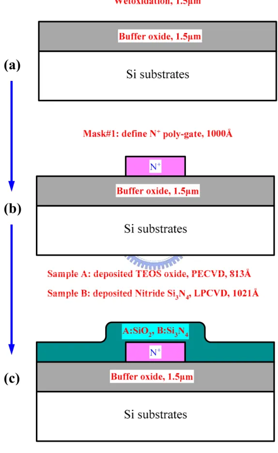
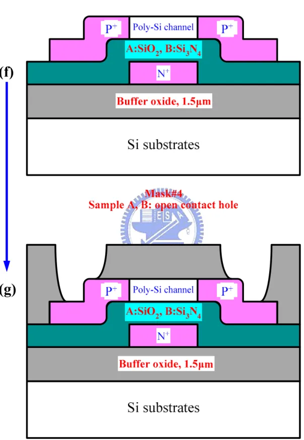
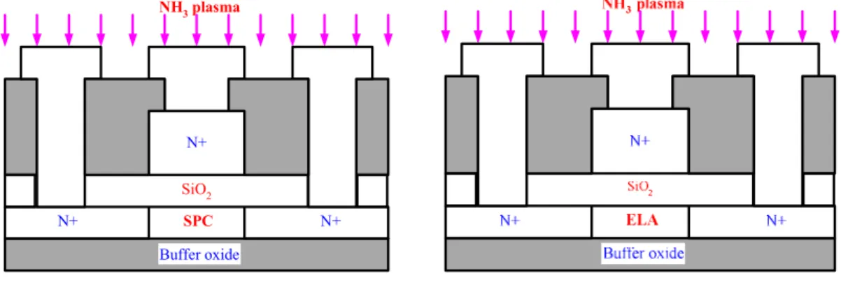
(17) [2-7]. As the drain voltage is further raised, the leakage current of the CMTFT shows higher current than conventional poly-Si TFT. This increase in leakage current is basically due to the turn-on the P+/i/N+ diode. It was reported that a significant reduction in leakage current in the thick drain structure is obtained compared to a thin drain structure [2-8]. This reduction in the leakage current is due to the reduction of the lateral electric field in the poly-Si TFT with thicker junction depth. However, thicker film devices have the disadvantages of larger grain-boundary trap density, lower mobility, and lower on-state current compared to thinner film devices [2-9]. For thin active layers [2-10], there is insufficient active layer thickness for complete band bending, resulting in less charges being trapped and hence an improvement in the density of state. This decrease in leakage current is due to the easier formation of a p-channel, which suppresses the generation volume more effectively. In this chapter, we try to understand how the defect reduction in the drain junction affects the leakage current of poly-Si TFTs. Variations of the drain junction before and after NH3 plasma treatment are characterized by Kelvin Probe Force Microscope (KFM).. 2.2 Experiment Details 2.2.1 Fabrication of bottom-gated P-type poly-Si TFTs using SPC 8.
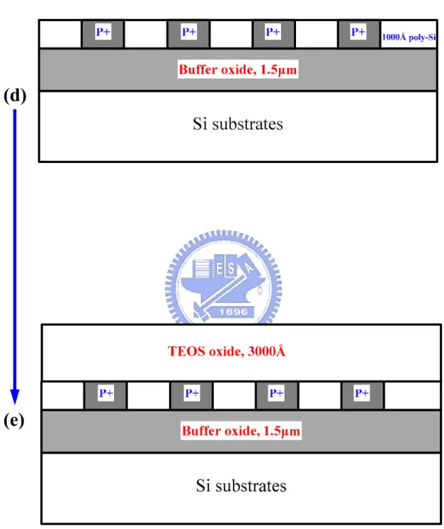
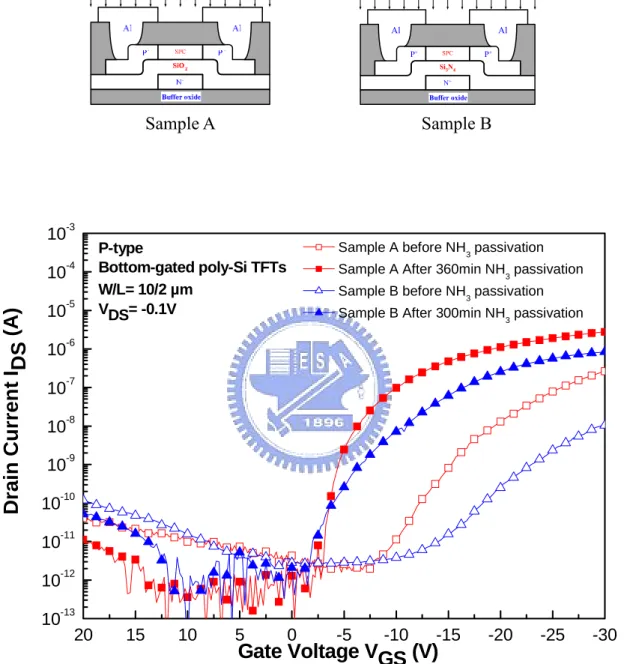
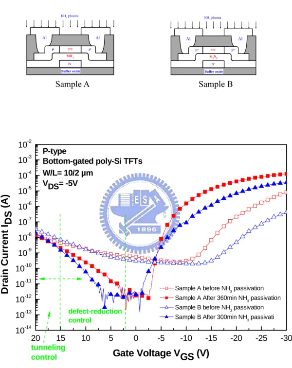
(18) crystallization Two types of samples were fabricated called Sample A (SiO2) and Sample B (Si3N4). The key process flows as shown in Fig. 2.1. A 1.5µm thermal Oxide was grown on bare Si wafer as a buffer layer. Then a phosphorous-doped α-Si of 1000Å was deposited at 550℃ in a low pressure chemical vapor deposition (LPCVD, vertical furnace) system. The phosphorous-doped α-Si film was annealed at 900℃ for 2 h and then patterned. A 813Å thick tetraethyl orthosilicate (TEOS) oxide layer was deposited by plasma enhance chemical vapor deposition (PECVD) system as a gate dielectric of sample A. A 1021Å thick nitride (Si3N4) layer was deposited by LPCVD system as a gate dielectric of sample B. A 91 nm α-Si layers were deposited as the active layers of sample A and B. Ion implantation was then performed to form the regions of source and drain using photoresists (P.R) as hard mask, afterward, furnace annealing at 600℃ for 24 h in N2 ambient was carried out to recrystallize the Si films. After defining the active regions, a 3000Å passivation TEOS SiO2 layer was deposited by LPCVD system. Finally, the contact holes were opened and the Al films were deposited and then defined. The detail process flows are listed as follow: 1. Initial RCA clean 2. 1.5µm thermal Oxide: wet oxidation, 978℃.. 9.
(19) 3. A phosphorous-doped α-Si layer of 1000Å was deposited in situ : vertical furnace, decomposed SiH4 gases, 550℃. 4. Thermal annealing at 900℃ for 2 h. 5. Mask #1: Gate pattern was defined and etched by anisotropic plasma etching. 6. P.R striped and side-wall polymers were removed by standard clean Ⅱ (SC-Ⅱ). 7. RCA cleaning without final HF-dip. 8. Sample A: A TEOS oxide (SiO2)layer of 813Å was deposited by PECVD at 350℃ as gate insulator. 9. Sample B: A nitride (Si3N4) layer of 1021Å was deposited by LPCVD at 600℃ as gate insulator. 10. Sample A and B: amorphous silicon layer of 910 Å were deposited by LPCVD at 550℃. 11. Sample A and B: mask #2, photoresists were defined for ion implantation. 12. Sample A and B: ion implantation, B, 15KeV, 1×1016 cm-2. 13. Sample A and B :Photoresists were striped. 14. Sample A and B: post-implantation annealing, 600℃, 24 hrs.. 10.
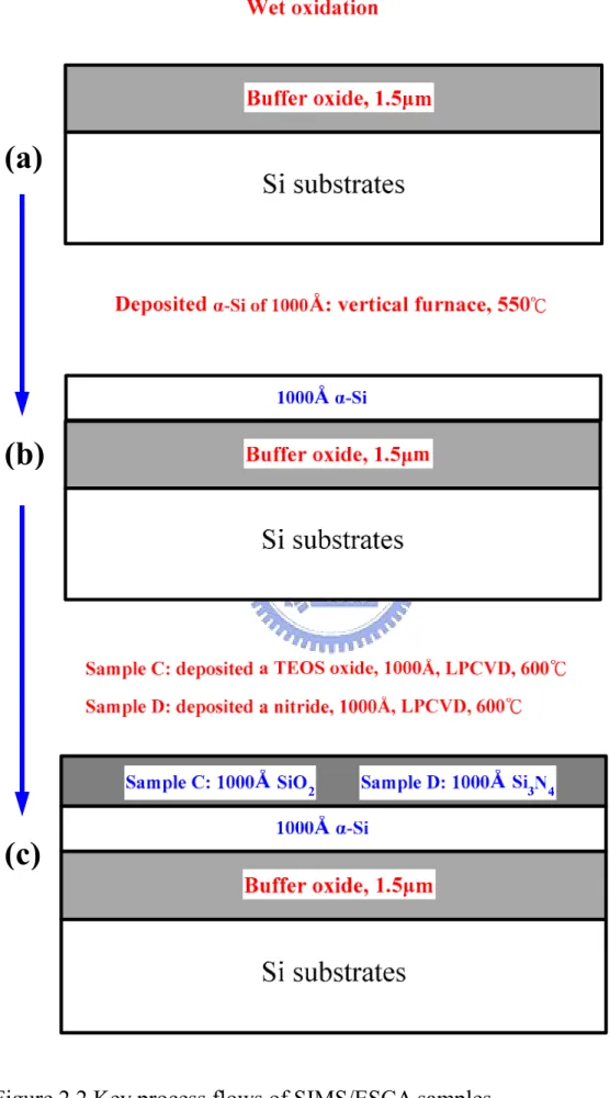
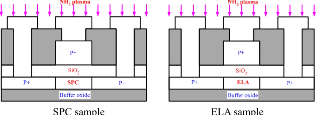
(20) 15. Sample A and B: mask #3, active region were defined and etched by PolyRIE. 16. Sample A and B : Photoresists were striped and RCA cleaning without final HF-dip. 17. Sample A and B: TEOS oxide passivation layers of 3000Å were deposited by LPCVD at 695℃. 18. Sample A and B: mask#4, opened contact hole by BOE wet etching. 19. Sample A and B: Photoresists were striped and dipped HF 20. Sample A and B: Al layer of 5000 Å were sputtered by thermal coater as electrodes. 21. Sample A and B: mask#5, defined Al pad. 22. Sample A and B: Al sintering, 400℃, 30min.. 2.2.2 Sample for ESCA/SIMS analysis Two types of samples were fabricated called Sample C (SiO2) and Sample D (Si3N4). The key process flows as shown in Fig. 2.3. A 1.5µm thermal Oxide was grown on the bare Si wafer as a buffer layer. Then a 1000Å α-Si was deposited at 550℃ in a LPCVD (vertical furnace) system. Sample C was deposited a 1000Å TEOS oxide by PECVD system. Sample D was deposited a 1021Å Si3N4 layer by LPCVD system. Both 11.
(21) sample C and D were deposited the 500Å amorphous Si layer by LPCVD system. Finally, a passivation TEOS SiO2 of 3000Å was deposited by LPCVD system. After NH3 plasma treatment for 4, and 8 h, the passivation oxides of both samples were removed by buffered oxide etching (BOE) solutions. The detail process flow is listed as flow: 1. Initial RCA clean 2. 1.5µm thermal Oxide: wet oxidation, 978℃. 3. A α-Si layer of 1000Å was deposited: vertical furnace, decomposition of SiH4 gases, 550℃. 4. Sample C: A TEOS oxide (SiO2) layer of 1000Å was deposited by LPCVD at 600℃. 5. Sample D: A nitride (Si3N4) layer of 1021Å was deposited by LPCVD at 600℃. 6. Sample C and D: A amorphous silicon layer of 500 Å were deposited by LPCVD at 550℃. 7. Sample C and D: RCA cleaning without final HF-dip. 8. Sample C and D: A TEOS oxide (SiO2) passivation layer of 3000Å was deposited by LPCVD at 695℃.. 12.
(22) 9. Sample C and D: NH3 plasma treatment with various time. 10. Sample C and D: A passivation layer (SiO2) was removed by BOE.. 2.2.3 Sample for Kelvin Probe Force Microscope (KFM) analysis Two types of samples were fabricated called Sample E (boron-doped). The key process flows as shown in Fig. 2.3. A 1.5µm thermal oxide was grown on the bare Si wafer as a buffer layer. A α-Si of 1000Å was then deposited at 550℃ in a LPCVD (vertical furnace) system. Sample E was implanted by born ions at an energy of 15KeV and dose of 1E16 cm-2. Finally, a 3000Å passivation TEOS SiO2 was deposited by LPCVD system. After NH3 plasma treatment of 6 h, the passivation oxide was removed by BOE solutions. The detail process flow is listed as flow: 1.. Initial RCA clean. 2.. 1.5 µm thermal Oxide: wet oxidation, 1050℃.. 3.. A α-Si layer of 1000Å was deposited: LPCVD, decomposition of SiH4 gases, 550℃.. 4.. Sample E: ion implantation, B, dose = 1E16 cm-2, 15 Kev.. 5.. RCA cleaning.. 6.. Post-implantation annealing, 600℃, 24hr. 13.
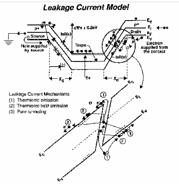
(23) 7.. A TEOS oxide (SiO2) passivation layer of 3000Å was deposited by LPCVD at 695℃.. 8.. NH3 plasma treatment of 6 h: 700sccm, 200W.. 9.. A passivation layer (SiO2) was removed by BOE.. 2.3 Results and Discussions: 2.3.1 Physical mechanism on the leakage current For a thin film transistor, the leakage current can be expressed as [2-2] − ( E − 2 ∆E ) ⎫ ⎧ qW (Te + Tp )εyVds ⎪ ⎪ KT IL = ⎨ Nste ⎬ (2-1) KT ⎪⎩ ⎪⎭ F0. where, q. is the electron charge.. W. is the channel width.. k. is the Boltzman’s constant.. T. is the temperature.. Te. is the electron tunneling probability.. Tp. is the hole tunneling probability.. εy. is a lateral electric field in the drain depletion region.. Nst. is the trap density (/cm3/eV) 14.
(24) EF0 ΔE. is approximately half the bandgap. is the drain grain boundary traps with respect to midgap.. The leakage current model: as electrons from valence band are captured by the traps via any of the three processes (i.e., thermionic emission, thermionic field emission, and tunneling), the holes generated are swept to the drain and they result in leakage current. For the trap to remain active, it must emit the captured electrons to the conduction band. Those electrons accumulate in the channel, and increase electrical potential with respect to source (assume source is grounded). As a result, these electrons flow into the source where they recombine with holes supplied by the ground. In equation (2-1), it can effectively reduce the leakage current by decreasing lateral electric field and effective grain boundary trap density at the channel/drain junction region. At a low drain field (-0.1V), the lowest activation energy is about Eg/2, thermionic emission is the dominate leakage mechanism at low field. This is the process step (1) in Fig. 2.4. As the drain bias increases (more negative), the drain depletion field increases and activation energy decreases. This suggests that the high field in the drain depletion region has reduced the barrier. As such, the dominant leakage current mechanism is thermionic field emission and is represented by process (2) in Fig. 2.4. Further increase of the drain bias put activation energy below 0.1eV. Since Ea < 0.1eV present almost no barrier to the carrier. 15.
(25) motion, the dominant leakage mechanism is pure tunneling.. 2.3.2 Hydrogenation effect on high-VDS leakage current and physical property analysis Fig. 2.5 (a) and (b) shows the transfer characteristics for comparison of bottom-gated poly-Si TFTs with SPC/ELA before and after NH3 plasma passivation at VDS= -0.1, and -5 V, respectively. After hydrogenation, the electrical characteristics of the three types of the poly-Si TFTs have been improved as listed in table 2.1. The minimum leakage current of sample A is decreased from 260 pA to 0.2 pA. Sample B is decreased from 196 pA to 0.15 pA. One can see that sample B after NH3 plasma passivation has a lower leakage current than that of sample A at high lateral electric fields (VDS= -5 V) as shown in Fig. 2.5 (b). This reduction in the leakage current is ascribed to defect reduction in the drain junction because nitrogen and hydrogen radicals can effectively accumulate at the Si3N4/channel interface as shown in Fig. 2.8 (a) and (b). In Fig. 2.8 (a), the peak value of nitrogen concentration in sample D (gate dielectric: Si3N4) is increased from 1.61×10¹⁸ to 4.38×10²¹ after NH3 plasma treatment of 8 h. It is obviously that [SiN] of sample D is remarkably larger than that of sample C (gate dielectric: SiO2) near the dielectric/channel interface. It is also interesting that the concentrations of SiN at Si3N4 layers are unchanged after NH3 plasma treatment of 4 h 16.
(26) and 8 h. Inversely, the concentration of SiN at SiO2 layers increases as comparing to sample D of 4 h and 8 h. In Fig 2.8 (b), we observed that the hydrogen concentration of sample D had a larger value than that of sample C after NH3 plasma treatment of 8 h, especially at the gate dielectric/channel interface. It is also interesting that [H] of sample D with NH3 plasma treatment of 4 h is about the same in the nitride layer as compared to NH3 plasma treatment of 8 h. Contrary to sample C, [H] with NH3 plasma treatment of 8 h is significantly increased in the oxide layer as compared that with NH3 plasma treatment of 4 h. This result implies that the nitride layer can effectively prevent nitrogen and hydrogen atoms from downward diffusing. Conversely, nitrogen and hydrogen atoms can diffuse into the oxide layer through the channel region via hydrogenation processes. As mentioned above, the numbers of hydrogen/nitrogen atoms in the channel region with Si3N4 as gate insulator is larger than that with TEOS SiO2 as gate insulator. Therefore, a bottom-gated poly-Si TFT with Si3N4 as gate insulator can further reduce defect states in the drain junction as well as at the channel/dielectric interface, and obtains lower leakage current at near zero gate bias. In KFM analysis, the difference of the surface potential between P+/i is 40 mV before NH3 plasma treatment as shown in Fig. 2.10. After NH3 plasma treatment of 6 h, it becomes 186 mV. As a result, the surface potential increases the magnitude of 146 mV resulting from NH3. 17.
(27) plasma treatment. In Fig. 2.11, the rises in the surface potential lead to increase the depletion width in the drain junction. This is attributed to that defect states before NH3 passivation can not generate carriers in the depletion region. After NH3 passivation, the passivated defects have abilities to generate active carriers resulting in extra depletion width. This result make further reduce the leakage current due to defect reduction in the drain junction. Hence, we proposed “defect-reduction controlled regime” in Fig. 2.5 (b). At a high drain field, the leakage current is dominated by tunneling mechanism and independent of the defect reduction. In other words, sample B and A have similar magnitude. of. the. leakage. current. at. high. drain. fields.. We. proposed. “tunneling-controlled regime”. However, grain-boundary defects results in deep states affecting the leakage current. In other words, fewer deep states cause lower leakage current. The similar phenomena with respect to the off-sate current were also found in Fig. 2.6 (b) and 2.7 (b). The electrical characteristics of p- and n-type top-gated poly-Si TFTs are respectively listed in Table 2.2 and 2.3. In comparison of the on-state currents (Fig. 2.5 (b)), Sample A has larger turn-on current than sample B after hydrogenation. The on-state current is dominated by donor-like tail states originated from strained bonds at the channel/dielectric interface. This is well known that stresses at the Si3N4/poly-Si interface are larger than the. 18.
(28) SiO2/poly-Si interface due to larger differences in thermal expansion coefficient between SiO2 and poly-Si. Although the larger number of hydrogen and nitrogen atoms are blocked at the Si3N4/poly-Si interface ( Fig. 2.8 (a), (b)) after NH3 plasma treatments, most of these atoms can easily passivate deep states originating from dangling bonds at the channel/dielectric interface. For this reason, the number of donor-like tail states at Si3N4/poly-Si interface after NH3 hydrogenation is still larger than at the SiO2/poly-Si interface. Therefore, the on-state current of sample A after NH3 hydrogenation is larger than that of sample B. In terms of the degree of the improved on-state current, Sample B (gate nitride) is higher than sample A (gate oxide) due to the larger number of hydrogen and nitrogen atoms are blocked at the Si3N4/poly-Si interface. For the conventional TFT using ELA techniques (Fig. 2.6 (b) and 2.7 (b)), the on-state current is almost same before and after NH3 plasma passivation. This slightly improvement is attributed to very small number of the donor-like tail states (i.e., in-grain defects) exist at the SiO2/poly-Si interface as well as within the channel.. 2.3.3 Hydrogenation effect on low-VDS leakage current and physical property analysis In a p-channel device, the leakage current at low VDS depends on the total density of states at midgap and on the density of states in the upper half of the gap [2-10]. For a 19.
(29) p-type TFT in low field regime, the leakage current of three types of samples all decrease after NH3 plasma passivation (Fig. 2.5 (a)). At such a low drain field, we found that the leakage current of the bottom-gated TFT (Fig. 2.5(a)) after hydrogenation is slightly decrease as compared to that of the top-gated TFT (Fig. 2.6(a) and Fig.2.7 (a)). This result suggests that the passivation path of the bottom-gated device is shorter than the top-gated device. For the bottom-gated TFTs, the number of the tail states within the channel can be further passivated by hydrogen and nitrogen atoms as compared to the top-gated TFTs. Therefore, the bottom-gated TFT still has a slightly reduction of the leakage current at a low drain field after NH3 hydrogenation. On the Contrary to top-gated TFTs, the leakage currents before and after NH3 hydrogenation are still independent of VGS as shown in Fig. 2.6 (a) and 2.7 (a). From previous works [2-7], thicker films produced by SPC or direct poly-Si deposition are known to exhibit a minimum (at VGS, min) in their transfer characteristic for low VDS, and for VGS < VGS, min the current becomes independent of VGS. In these conditions, the contribution of thermally-generated carriers becomes dominant. As a result, we suggest that the leakage currents of bottom-gated TFTs at a low drain field still depend on defect reduction, not independent of VGS. In an undoped polysilicon TFT, the flat band voltage (VFB) is essentially the gate. 20.
(30) voltage at which the induced charges equal the trapped charges [2-11]. In Fig. 2.5 (b) and 2.6 (b), VFB began at more negative gate bias before hydrogenation and then moved toward near zero gate bias. It shown that there is a larger density of traps at the dielectric/channel interface as well as within the channel, and a more negative gate bias induces larger concentration of the holes filling with the larger traps before hydrogenation. After hydrogenation, VFB is approximately at zero gate bias, indicating that the reduction of trap density can be completely filled with smaller concentration of holes. Fig. 2.7 (a) and (b) show the transfer characteristics for comparison of n-type top-gated poly-Si TFTs using SPC/ELA before and after NH3 plasma passivation at VDS= 0.1, and 5 V, respectively. In a low drain field, the leakage current before and after NH3 hydrogenation is independent of VGS and density of states. Contrary to a high drain field, the leakage current before and after NH3 plasma passivation is dependent of VGS and density of states. At a lower field, the leakage current is dominated by thermionic emission, while thermionic field emission and tunneling become dominant at a higher field.. 2.4 Summary Thermionic emission is the dominate leakage current mechanism at a low drain 21.
(31) field (VDS= -0.1V) while thermionic field emission dominate at moderately high drain field. At high drain bias (VDS> -5 V), tunneling was observed to be responsible for leakage current mechanism. We can effectively reduce the leakage current by decreasing lateral electric field and effective grain-boundary trap states in the drain junction, especially in the deep states. From SIMS analysis, we found that a Si3N4 layer as the gate insulator of bottom-gated TFTs effectively attains an accumulation of hydrogen and hydrogen atoms within the channel region after NH3 plasma treatment as compared to a SiO2 layer as the gate insulator of bottom-gated TFTs, indicating a reduction of more deep states in the channel region. As a result, Si3N4 is a diffusion barrier for nitrogen and hydrogen radicals. After NH3 plasma treatment, we also verified that the increasing depletion width results from raising the surface potential by using KFM analysis. The increasing depletion width implies defect reduction in the drain junction and causes further reduction of the leakage current. Hence, we propose “defect-reduction controlled regime”. When the leakage current approaches to together, we call “tunneling controlled regime”. After NH3 plasma hydrogenation, the p-type bottom-gated TFT with Si3N4 dielectric not only further reduces the leakage current at a high drain field (VDS= -5V) as compared to the TFT with SiO2 dielectric but also slightly decreases at a low drain field.. 22.
(32) The leakage current strongly depends on the number of the acceptor-like deep states at positive gate bias. We also found that the leakage current of the bottom-gated TFT has a slightly reduction at a low field after NH3 plasma passivation. Contrary to the top-gated TFT, the leakage current is independent of VGS after NH3 plasma passivation. We suggest that the bottom-gated TFT has a shorter diffusing path of hydrogen diffusion than the top-gated one, and obtains the higher degree of reducing deep states. Therefore, the bottom-gated TFT still has a slightly reduction of the leakage current at a low drain field after hydrogenation.. 23.
(33) Chapter 3. Influence of Long-time NH3 Plasma Treatment on the Electrical Characteristics of Poly-Si TFTs. 3.1. Introduction Poly-Si TFTs are widely used in various applications, and will figure prominently. in future high-resolution, high-performance flat-pannel display (FPD) technology [3-1]. Poly-Si TFTs as peripheral driver circuits can be directly integrated onto AMLCD substrates. High-performance poly-Si TFTs are capable of improving display reliability by reducing connections to external chips and make manufacturing costs down by reducing externally required chips. In poly-Si TFTs, however, grain boundaries and intragrain defects bring a profound influence on device characteristics and carrier transport. It is well known that hydrogenation tends to terminate the grain-boundary dangling bonds with hydrogen, remarkably improving the electrical characteristics of poly-Si TFTs, especially in leakage current (Ioff), subthreshold swing (SS), threshold voltage (Vth) [3-2]. Hydrogenation is a well-accepted technique for reducing trap state densities. 24.
(34) at SiO2/poly-Si interface and grain boundaries of the poly-Si channel films, thereby lowering the grain boundaries potential barrier. Hydrogenation by plasma discharge [3-3]-[3-4], by the deposition of hydrogen-containing nitride film [3-5], or by H+ ion implantation [3-6] have been reported to improve the performance of poly-Si TFTs. In general, the activation energy for diffusion of an impurity along a grain boundary is lower than that for diffusion within the lattice [3-7]. Consequently, grain boundaries could be expected to act as “diffusion pipes” for the rapid migration of hydrogen into polycrystalline silicon. It is further shown that an oxide overlayer significantly attenuates the concentration of H that enters the poly-Si from a plasma discharge. As a result, hydrogen from the plasma can diffuse into the active channel region by several possible pathways (A1~A4) as shown in Fig. 3.1. High diffusion rates in poly-Si grain boundaries prefer path A1 and A2 while a reduced diffusion favors A2 and A4. However, it had been shown that the hydrogenated poly-Si TFTs suffer a low hot-carrier endurance [3-8] [3-9] and a low thermal stability. Hydrogen passivation is stable at 150℃, channel hot-electron stress at high temperature appears to create additional grain-boundary traps, by breaking Si-H bonds at grain boundaries of the drain junction. The acceptor-type fast interface states are generated by hot-electrons, which break Si-H bounds at the interface as well as at the grain boundary. In order to meet the requirement. 25.
(35) of integrating fabrication of the entire display circuitry (i.e., LCD’s driver and active matrix elements) into glass substrates, the device parameter of the poly-Si TFTs must be optimized. Choi et al. exhibited that the grain boundary and in-grain defects result in the continuous distribution of trap states in the forbidden bandgap [3-10]. The deep states, which originate from the dangling bonds in grain boundaries, influence the threshold voltage (Vth) and the subthreshold swing (SS). The tail states, which originate from the in-grain defects, affect the field-effect mobility (µFE) and the leakage current (Ioff). Because of the density of the in-grain defects in the low temperature SPC poly-Si TFTs is very high, it takes a long time to accumulate the sufficient concentration of hydrogen to eliminate the trap states, especially in tail states. However, many reports have been proposed that NH3 plasma and H2 plasma treatment both can effectively promote the performance of poly-Si TFTs, but further improvement in NH3 plasma passivation [3-11]. Poly-Si TFTs after NH3 plasma treatment obtain better device performances, including a dearease of the leakage current (Ioff), an increase of the field-effect mobility (µFE), a decline of the subthreshold swing (SS) and an improvement on/off current ratio (Ion/Ioff) than those after H2 plasma treatment. These further improvements are attributed to the atomic hydrogen passivating. 26.
(36) the dangling bonds and in-grain defects, to the nitrogen piling up at SiO2/channel interface, and to the strong Si-N bond terminating the dangling bonds at the grain boundaries as well as inside the grain. In this chapter, we investigate the influence of long-time NH3 plasma treatment on the electrical characteristics of poly-si TFTs.. 3.2. Experiments for Long-time NH3 Plasma Treatment. 3.2.1 Fabrication of bottom-gated poly-Si TFTs using SPC processes Two types of samples were fabricated called Sample A (SiO2) and Sample B (Si3N4). A 1.5 µm thermal Oxide was grown on bare Si wafer as a buffer layer. Then a phosphorous-doped α-Si of 1000Å was deposited at 550 ℃ in LPCVD system. The phosphorous-doped α-Si film was annealed at 900 ℃ for 2 h and then patterned. A 813Å thick TEOS oxide was deposited by PECVD system as a gate dielectric of sample A. A 1021Å thick Si3N4 layer was deposited by LPCVD system as a gate dielectric of sample B. A 910 Å α-Si layers were deposited as the active layers of sample A and B. After defining photoresists, sample A and B was implanted (Boron, 15 KeV, 1×1016 cm-2) to form the source and drain, and then furnace annealing at 600℃ for 24 h in N2 ambient was. carried out to recrystallize the Si films. After defining the active regions,. a 3000Å passivation TEOS SiO2 was deposited by LPCVD system. Finally, the contact holes were opened and the Al films were deposited and then defined. NH3 plasma 27.
(37) passivation was performed in a parallel-plate plasma reactor at 350℃ with a RF power of 200 W, 300 mTorr, and 700 sccm. As mentioned above, key process flows are illustrated in Fig. 3.2.. 3.2.2 Fabrication of top-gated poly-Si TFTs using SPC/ELA processes The poly-Si TFTs were fabricated on the thermally oxidized silicon wafer. A 1000 Å thick α-Si was deposited at 550 ℃ by LPCVD, and then sample D and E were annealed at 600 ℃ for 24 hr in N2 ambient. Sample F and G were crystallized into poly-Si films by a KrF excimer laser irradiation in vacuum (~10-3 Torr) at room temperature with an energy density of 390 mJ/cm2. After defining the active islands, a 1000Å TEOS SiO2 was deposited by the LPCVD. Another 3000 Å of thick amorphous Si was deposited at 550 ℃ by LPCVD system and patterned as gate electrodes. A self-align ion implantation was performed to form source, drain, and gate electrodes (for sample D and F: phosphorus, 35 KeV, 1×1016 cm-2; for sample E and G: Boron, 15 KeV, 1×1016 cm-2). After post-implantation annealing, a 3000Å passivation TEOS SiO2 was deposited by LPCVD system. Finally, the contact holes were opened and the Al films were deposited and then defined. NH3 plasma passivation was performed in a parallel-plate plasma reactor at 350℃ with a RF power of 200 W, 300 mTorr, and 700 sccm. As mentioned above, key process flows are illustrated in Fig. 3.3. 28.
(38) 3.3. Results and Discussions. 3.3.1. Hydrogenation. effects. on. the. threshold. voltage. and. subthreshold swing The threshold voltage is defined as the gate voltage at a fixed drain current IDS = IDN × (W/L), where IDN is a normalized drain current [3-12]. Vth is affected by the total number of active trap states between the bulk Fermi-level and the surface Fermi-level position. The bulk Fermi level is slightly above midgap since undoped polysilicon is slightly n-type. For conventional top-gated poly-Si, Vth and SS are improved without an obvious hydrogenation onset period. These two parameters are more sensitive to the deep states near midgap [3-12]. In terms of the passivation rate in SS (Fig. 3.4), both of SiO2 and Si3N4 samples reach the saturation region after NH3 plasma passivation of 30 min, indicating NH3 plasma passivated the deep states is faster than tail states. From SIMS analysis, the concentration of H and N atoms for Si3N4 dielectric inside the channel is comparable to that of SiO2. Hence, SS for Si3N4 dielectric can achieve saturation region as soon as SiO2 dielectric due to pre-dominating by the deep states within the channel. Here the effects of the interface states were assumed to be negligible because of the much higher bulk defect density presenting in polysilicon. It is also noted that poly-Si TFTs with Si3N4 dielectrics have larger saturated value of SS than that of. 29.
(39) SiO2 dielectrics (Fig. 3.4). After most of deep states within the channel are compensated, the saturating SS is dominated by the number of dangling bonds at the insulator/channel interface. This is well known that Si3N4 has larger interface states than SiO2 due to larger stresses existing in the Si3N4/poly-Si interfacee. For p-type bottom-gated TFTs using SPC processes, Vth (passivation curves of SiO2 dielectric) reach saturations at 90 min as shown in Fig. 3.5 (a). It implies that the numbers of deep states in the bulk oxide are compensated by H atoms, leading to a faster passivation rate. Contrary to use Si3N4 dielectrics, Vth is continuously improved by NH3 plasma treatment without saturation. This result is consistent with SIMS analysis. The significantly accumulation of nitrogen and hydrogen radicals reduces the more deep states within the channel. Although the number of dangling bonds within the channel is almost equal as fabricated, Si3N4/poly-Si interface has lager deep states than SiO2/poly-Si interface. As a result, the bottom-gated TFT with Si3N4 dielectric has a larger saturated value of Vth. We also found that poly-Si TFTs using ELA processes have the fastest passivation rate (i.e., 30 min). This is because ELA processes result in fewer number of the deep states than that of SPC processes. Similar response in Vth was founded in Fig. 3.5 (b) an (c).. 3.3.2. Hydrogenation effects on the field-effect mobility and the 30.
(40) leakage current At the turn-on condition near Vth, μFE (for n-type) is strongly influenced by the density of trap states at or above the surface Fermi-level position (the bulk Fermi level away from the interface plus the surface potential) above mid-gap [3-12]. The number of strained bonds is roughly a factor of 100 more than the number of dangling bonds at a grain boundary. Hydrogen bonding in dangling bonds is far stronger than to the strained bonds (above 2eV greater binding energy than the bond-centered interstitial site) [3-14]. Hence, during passivation, as hydrogen traps and detraps at various sites, it will remain in dangling-bond sites for a significantly longer period than the tail states. Only when the hydrogen concentration is as large as to fill both the deep dangling bond states and the tail states will significant fraction of the tail states be passivated. It takes time to accumulate the necessary concentration of hydrogen. In Fig. 3.6 (a), the mobility increases to the saturation point after NH3 plasma passivation of 90 min for SiO2 dielectrics. In other words, a Si3N4 layer has a slower hydrogenation rate than SiO2 dielectric. According to analytic results of SIMS, using Si3N4 as the gate dielectric has a larger accumulation of hydrogen and nitrogen atoms at the interface but is slightly smaller concentrations within the channel. The donor-like tail states are weakly passivated by significant number of hydrogen and nitrogen atoms. It means that the. 31.
(41) mobility is still dominated by the donor-like tail states at the interface in this case. For using Si3N4 as gate insulator, the field-effect mobility continuously increases without saturation occurs. It is described to Si3N4 resist nitrogen and hydrogen radicals downward diffusing. Therefore, the further reduction of the tail states was obtained and the field-effect mobility continuous improves. It is also found that poly-Si TFTs using SPC processes have slower hydrogenation rate than that of ELA processes as shown in Fig. 3.6 (b). The propagation of nitrogen and hydrogen radicals inside the grain is slower than that at the grain boundary due to lower binding energy in the tail states. However, SPC processes result in larger tail state densities than ELA processes [3-10], hence nitrogen and hydrogen radicals need a longer time to passivate the tail states of poly-Si TFT using SPC processes. Similar phenomena are also found in Fig. 3.6 (c).. Because of strong dependence of the leakage current with positive gate bias (for p-type) via band-tail assisted thermionic-field emission, the minimum current denotes the dominating carrier transport changing from electrons to holes as VGS is increased more negative. At the minimum leakage current (with VGS closest to the subthreshold regime), the conduction and valence bands are nearly flat, with the Fermi level positioned at about mid-gap. The majority of holes are trapped at mid-gap grain boundary states (above the Fermi level) [3-15]. For using Si3N4 and SiO2 as gate 32.
(42) dielectric, reduction of the minimum leakage current has an almost same passivation rate (i.e., reaching the saturation point at the same time) as shown in Fig. 3.7 (a). We suggest that most of the acceptor-like tail states exist in the channel region near the drain, dominating the minimum leakage current. We also found that the saturation time of acceptor-like tail states is shorter than that of donor-like tail states by comparing Si3N4 curve of Fig. 3.7 (a) and 3.6 (a). Contrary to oxide, both of two tail states have almost same saturation time. The previous study [3-13] suggests that the donor-like tail states close to valance band (governing turn-on mobility) and acceptor-like tail states close to conduction band (influencing the leakage current) are responding to plasma hydrogenation at approximately the same rate with the same onset period. For bottom-gated TFTs using Si3N4 dielectrics, the donor-like tail states is larger at the interface than that of oxide. Hence, it needs a longer time to passivate such defects.. 3.3.3 Hydrogenation effects on the effective trap density The trap density, which can be determined by the theory established by Levinson et. al. [3-16], is based on Seto’s theory [3-17]. For a thin film transistor, the source-drain current IDS can be given as following:. I DS. ⎛ − q 3 N t 2t W = CoxVDS µ FEVGS exp⎜ ⎜ 8ε si kTCoxVGS L ⎝. where,. 33. ⎞ ⎟ ----------------------(Eq. 3-1) ⎟ ⎠.
(43) μFE. is the field-effect mobility of the carriers.. q. is the electron charge.. K. is the Boltzmann’s constant.. T. is the temperature.. Nt. is the trap-state density per unit area.. t. is the channel thickness.. This expression, first developed by Levinson et al., is a standard MOSFET’s equation with an activated mobility, which depends on the grain boundary barrier height as introduced by Seto. Levinson et al. assumed that the channel thickness was constant and equal to the thickness of poly-Si film. This simplifying assumption is permissible only for very thin film (t < 100 Å). The trap-state density can be obtained by extracting a straight line on the plot of ln(IDS/VGS) versus 1/VGS at low source-drain voltage and high gate voltage. Proano et al.[3-15] thought that a better approximation is to calculate the gate induced carrier channel thickness by solving Poisson’s equation for an undoped material and to define the channel thickness as a thickness which 80 percent of the total charge induced by the gate. Doing so, one obtains. t ch. ⎧⎪ ε Si ⎫⎪ 8 kTt ⎨ ⎬ ox ε SiO ⎪⎭ ⎪⎩ -------------------------------------------------------(Eq. 3-2) = q(VGS − VFB ) 2. 34.
(44) , which varies inversely with (VGS-VFB). This predicts, by substituting Eq. 3-2 into Eq. 3-1, that ln[IDS/(VGS-VFB)] varies linearly with 1/(VGS-VFB)2. We used the gate voltage at which minimum leakage current occurs as the VFB. Then, Effective trap-density Nt can be determined from the square root of the slope.. Nt =. 1 ⎞4. Cox ⎛⎜ ε Si ⎟ q ⎜⎝ ε SiO ⎟⎠. slope --------------------------------------------------(Eq3-3). 2. Since the characteristics of poly-Si TFTs are very sensitive to the distribution of the trap states. The deep states is generated from the dangling bonds located mainly at the grain boundaries, while the tail states is caused by the stain bonds of in-grain defects inside the grain. For a SiO2 dielectric, the effective trap density is dramatically decreased from 1.13×10¹³ to 3.78×10¹² after 90min NH3 plasma passivation and becomes saturated condition as shown in Fig. 3.8 (a). However, for a Si3N4 dielectric, the effective trap density decreased from 1.77×10¹³ to 1.04×10¹³ after 300 min NH3 plasma passivation. As a result, it is obviously that the effective trap density continuously reduced by blocking hydrogen and nitrogen atoms. Contrary to ELA sample, we also found that the effective trap density is rapid down to saturation region due to less defect states as fabricated. For top-gated devices, ELA processes also have a faster hydrogenation rate than SPC processes (Fig. 3.8 (b)).. 35.
(45) 3.4. Summary In general, we have been known that threshold voltage and subthreshold swing. being affected the numbers of the deep states in the channel. For bottom-gated poly-Si TFTs with Si3N4 as a gate insulator, SS has a fast passivation rate as soon as SiO2 dielectrics. The interesting phenomena result from effectively accumulation of H and N atoms in the channel region, and causing significantly reduction of the dangling bonds within the channel. In terms of Vth, the slower passivation rate of Si3N4 dielectric was found than that of SiO2 dielectric. The H and N atoms can downward diffuse into oxide region and compensate oxide charges in bulk SiO2 because the passivation rates for oxide and nitride inside the channel are roughly identical. Contrary to Si3N4 dielectrics, most of H and N atoms are blocked within the channel. Hence, no saturations were found in improving Vth during NH3 plasma passivation. For the top-gated TFTs, the passivation rates of Vth are dominated by channel qualities. ELA processes have the faster passivation rates than SPC processes due to fewer numbers of the dangling bonds. The field-effect mobility of using Si3N4 as a gate insulator has a slower passivation rate than that of the SiO2 dielectric. The donor-like tail states for using Si3N4 dielectric are difficultly passivated by significant concentration of hydrogen and nitrogen atoms. It means that the field-effect mobility is still dominated by the donor-like tail states at the. 36.
(46) interface, in other words, the mobility is weakly depend on substantial incorporation of hydrogen and nitrogen atoms. But for Si3N4 dielectrics, the field-effect mobility continuously improves without saturations during NH3 plasma passivation. In terms of the minimum leakage current, both of Si3N4 and SiO2 dielectrics have nearly fast passivation rates. Because the minimum leakage current originates from the acceptor-like tail states near the drain junction within the channel, indicating same reduction rates of the tail states in the drain junction. We also found that top-gated poly-Si TFTs using ELA processes have the faster passivation rate in mobility and the minimum leakage current. Nt represents the total effective trap states exist in the channel region when fully on state. Consisting with SIMS analysis, Si3N4 dielectrics observed that the effective trap density continuously reduced by blocking hydrogen and nitrogen atoms when passivation time further increasing. Contrary to SiO2 dielectrics, Nt achieved the saturation regime after NH3 plasma passivation of 90 min due to H and N atoms can downward diffuse into oxide layer. For ELA processes, Nt still has a faster passivation rate than SPC because of fewer defects present.. 37.
(47) Chapter 4. Conclusions. 4.1 Conclusions In this thesis, we utilized Si3N4 and SiO2 as the insulator of bottom-gated poly-Si TFTs to investigate the reduction of the leakage current by NH3 plasma treatment. Furthermore, we also investigated influences of long-time NH3 plasma treatment on the electrical characteristics of poly-Si TFTs. For a p-type poly-Si TFT, the leakage current strongly depends on the number of acceptor-like deep states under positive gate bias. After NH3 plasma passivation, the bottom-gated TFT using Si3N4 as the gate insulator not only reduces the leakage current at a high drain voltage (VDS= -5V) as compared to the bottom-gated TFT using SiO2 as the gate insulator, but also slightly decreases in the leakage current at a low drain bias (VDS= -0.1 V). From SIMS analysis, a Si3N4 layer underneath poly-Si channel can effectively make hydrogen and nitrogen atoms accumulate within the channel. In the other words, Si3N4 is a diffusion barrier for nitrogen and hydrogen radicals. We also observed the variation of band diagram in the drain junction with KFM. Consequently,. 38.
(48) the increasing depletion width indicates defect reduction in the drain junction leading to improve the leakage current. After NH3 plasma passivation, the leakage current of poly-Si TFTs using Si3N4 as the insulator of bottom-gated poly-Si TFTs was about one order of magnitude lower than that using SiO2 as the insulator of bottom-gated poly-Si TFTs. We say that defect-reduction control dominates the difference of the leakage current. When two of the leakage currents approach to together at high drain fields, the tunneling control is responsible for the mechanism. In general, we have been known that the threshold voltage and the subthreshold swing are affected by the number of the deep states in the channel. For bottom-gated poly-Si TFTs with Si3N4 as the gate insulator, SS has a fast passivation rate as soon as using SiO2 as insulator of bottom-gated poly-Si TFT. In the initial stage, it implies that the passivation rates of the deep states inside the channel are roughly identical for SiO2 and Si3N4 films. But in terms of Vth, it has a slower passivation rate than using SiO2 as the insulator. This result is suggests that hydrogen and nitrogen atoms can downward diffuse into oxide layer, and oxide charges are compensated by these atoms in bulk SiO2. Contrary to use Si3N4 dielectrics, Vth is continuously improved by NH3 plasma treatment without saturation. This result is consistent with SIMS analysis. The significantly accumulation of nitrogen and hydrogen radicals reduces the more deep. 39.
(49) states within the channel. We also found that top-gated poly-Si TFTs using ELA techniques obtained the faster passivation rate in Vth as compared to SPC ones due to fewer dangling bonds as devices are fabricated. The mobility of poly-Si TFT with Si3N4 as the bottom-gated insulator has a slower passivation rate than that of using SiO2 as the bottom-gated insulator. It means that the mobility of the bottom-gated TFT is still dominated by the number of donor-like tail states at the interface as devices are fabricated. As a result, using Si3N4 films with NH3 plasma treatment needs a longer time to passivate those defects at the interface. For using Si3N4 as gate insulator, the field-effect mobility continuously increases without saturation occurs. It is described to Si3N4 resist nitrogen and hydrogen radicals downward diffusing. Therefore, the further reduction of the tail states was obtained and the field-effect mobility continuous improves. However, in terms of the minimum leakage current, both of Si3N4 and SiO2 dielectrics have nearly fast passivation rates. Because the minimum leakage current originates from acceptor-like tail states in the drain junction, it indicates same defect-reduction rates of the tail states in the drain junction with short-time NH3 plasma treatment. When long-time NH3 plasma is applied, the leakage current of poly-Si TFTs with Si3N4 as bottom-gated insulator has a lower value at more positive gate bias than that of using SiO2 as the bottom-gated insulator.. 40.
(50) We also shown that top-gated poly-Si TFTs using ELA processes have faster passivation rates in mobility and in the minimum leakage current than that of using SPC processes. Nt represents the total effective trap states existing in the channel region when devices are biased under on state. Consisting with SIMS analysis, using Si3N4 films underneath poly-Si channel has a continuously reduction of effective trap density with long-time NH3 plasma treatment. Contrary to SiO2 dielectrics, Nt achieves the saturation region after NH3 plasma treatment of 90 min. As mentioned above, using Si3N4 films underneath poly-Si channel is good for poly-Si TFTs by long-time NH3 plasma treatment.. 4.2 Future Works It is the future trend for AMLCDs to fabricate low temperature poly-Si TFTs on low-cost glass substrates. For LTPS TFTs using ELA techniques, there are still some problems which shold be solved. We introduce these issues in three parts: (1) Improving the surface roughness: The surface roughness increases with increasing laser energy density and cause degradation of off-state current and reliability for the ELA poly-Si TFTs [1-25]. Meanwhile, the gate oxide can not scale down due to the surface roughness enhances local electric fields in the oxide. We suggest that CMP and etching-back 41.
(51) Chapter 3 Influence of Long-time NH3 Plasma Treatment on the Electrical Characteristics of poly-Si TFTs 3.1 Introduction. •••••••••••••••••••••••••••••••••••••••••••••••••••••••••••••••••••••. 24. 3.2 Experiments for Long-time NH3 Plasma Treatment 3.2.1 Fabrication of bottom-gated poly-Si TFTs using SPC processes. •••••••••••27. 3.2.2 Fabrication of top-gated poly-Si TFTs using SPC/ELA processes. •••••••••• 28. 3.3 Results and Discussions 3.3.1 Hydrogenation effects on the threshold voltage and subthreshold swing •••••29 3.3.2 Hydrogenation effects on the field-effect mobility and the leakage current. ••••••••••••••••••••••••••••••••••••••••••••••••••••••••••••••••••••• 30. 3.3.3 Hydrogenation effects on the effective trap density. 3.4 Summary. •••••••••••••••••••••• 33. •••••••••••••••••••••••••••••••••••••••••••••••••••••••••••••••••••••••••. 36. Chapter 4 Conclusions 4.1 Conclusions 4.2 Future Works. •••••••••••••••••••••••••••••••••••••••••••••••••••••••••••••••••••••. 38. •••••••••••••••••••••••••••••••••••••••••••••••••••••••••••••••••• 41. References. •••••••••••••••••••••••••••••••••••••••••••••••••••••••••••••••••••••••••••. 43. Table List. ••••••••••••••••••••••••••••••••••••••••••••••••••••••••••••••••••••••••••. 51. Figure List. •••••••••••••••••••••••••••••••••••••••••••••••••••••••••••••••••••••••••• 53. Publications. •••••••••••••••••••••••••••••••••••••••••••••••••••••••••••••••••••••••••• 94. Vita. ••••••••••••••••••••••••••••••••••••••••••••••••••••••••••••••••••••••••••. v. 95.
(52) techniques may be candidates for solving surface roughness. (2) Lowering the leakage current: poly-Si TFTs with high off-state current degrade the contrast ratio of display because of the loss of video information before the frame is being refreshed. Reducing the numbers of the trap states in the drain junction and decreasing the lateral electric field near the drain junction are effective ways to reduce the leakage current. (3) Avoiding device-to-device variation: a random distribution of grain boundaries in the channel makes a great impact on the uniformity of device. performance.. To. further. control. the. performance. of. laser-crystallized poly-Si TFTs, the number of grain boundaries in the drain junction has to be considered.. 42.
數據
+7
Outline
Hydrogenation effect on high-V DS leakage current and physical property analysis
Hydrogenation effect on low-V DS leakage current and physical property analysis
Hydrogenation effects on the threshold voltage and subthreshold swing
Hydrogenation effects on the effective trap density
Influence of Long-time NH3 Plasma Treatment on the
The electrical characteristics of n-type top-gated poly-Si TFTs using SPC/ELA techniques before and after NH 3 plasma hydrogenation
相關文件
Reading Task 6: Genre Structure and Language Features. • Now let’s look at how language features (e.g. sentence patterns) are connected to the structure
Magnetic fields in a tokamak - the toroidal field is generated by external coils, poloidal by electric current in the
雙極性接面電晶體(bipolar junction transistor, BJT) 場效電晶體(field effect transistor, FET).
▫ Not only the sentences with high importance score based on statistical measure should be considered as indicative sentence... Proposed
Biases in Pricing Continuously Monitored Options with Monte Carlo (continued).. • If all of the sampled prices are below the barrier, this sample path pays max(S(t n ) −
Put the current record with the “smaller” key field value in OutputFile if (that current record is the last record in its corresponding input file) :. Declare that input file to be
Set up the air current one wind speed it change with wind direction,flow for windbreaks during flowing field instead of after building, air current materials to
Several methods that modulation effective work function to maintain p-type gate material is the direction of future research, sush as microwave annealing with plasma
