國
立
交
通
大
學
電機學院 電機與控制學程
碩
士
論
文
應用在全載範圍高效率直流對直流升壓轉換器的電
流模式合成控制技術
Current-Mode Synthetic Control (CSC) Technique for
High Efficiency DC-DC Boost Converters Over a Wide
Load Range
研 究 生:陳逸群
指導教授:陳科宏 博士
應用在全載範圍高效率直流對直流升壓轉換器的電流模式合成控
制技術
Current-Mode Synthetic Control (CSC) Technique for High Efficiency
DC-DC Boost Converters Over a Wide Load Range
研 究 生:
陳逸群
Student:Yi-Chun Chen
指導教授:陳科宏 Advisor:Ke-Horng Chen
國 立 交 通 大 學
電控工程研究所
碩 士 論 文
A Thesis
Submitted to Department of Electrical Control Engineering
College of Electrical Engineering
National Chiao Tung University
in partial Fulfillment of the Requirements
for the Degree of
Master
in
Electrical and Control Engineering
October 2010
Hsinchu, Taiwan, Republic of China
i
應用在全載範圍高效率直流對直流升壓轉換器的電流模式合成控
制技術
研究生:陳逸群
指導教授:陳科宏博士
國立交通大學
電控工程研究所
摘 要
可攜式電子產品如手機、膝上型電腦和不同的多媒體設備使用電池作為主要能源。 為了要延長電池壽命,攜帶式的裝置在待機時會進入睡眠模式,因此需要快速喚醒時 間。所以快速的暫態響應和全載範圍維持高效率是常被要求的規格。 近年來,合成波調變機制常被用來增加系統的噪音餘度,使系統近乎一個無雜訊的 漣波且系統的負載穩壓也可以藉由誤差放大器加入而提升。但是他導致系統包含了兩個 極點而需要較複雜的補償方式。所以,本論文提出一個包含電流資訊的技術來簡化補償 方式。 本論文提出一個運用在升壓轉換器的電流模式合成控制技術(current-mode synthetic control technique)可以加速升壓轉換器的暫態響應速度並在全載範圍維持高的轉換效 率。這個技術類似於電流模式控制可以達到高的負載穩壓而且簡化電路不需要額外斜率 補償機制。除此之外,由於類似遲滯電流模式控制,系統暫態響應可以提升。輕載時, 由於與負載相關的頻率可達到高轉換效率。實驗結果顯示,載變化在0A 到 400mA 時, 輸出電壓的漣波可以維持在小於50mV 且在負載在 10mA 時效率可以達到 90%以上。關鍵字:遲滯電流調變控制(modulated hysteretic current control),暫態響應(transient response),波寬調變(pulse frequency modulation)
ii
Current-Mode Synthetic Control (CSC) Technique for High
Efficiency DC-DC Boost Converters Over a Wide Load Range
Student: Yi-Chun Chen Advisor: Dr. Ke-Horng Chen
Institute of Electrical Computer Engineering
National Chiao-Tung University
Abstract
Portable electronics products such as cellular phones, laptops and diverse multimedia equipments use battery as the main power source. To extend battery life, portable devices stay in sleep mode with a very low static current but require a fast wake-up to reach the normal mode with a much higher operational current. Therefore, the suitable converter for the portable devices needs fast transient response from the standby mode to the normal mode, meanwhile, high efficiency is guaranteed over a wide range.
Recently, the synthetic-ripple modulator (SRM) is proposed to improve the noise immunity through the synthetic current ripple, which is a nearly noise-free ripple signal. The accuracy also can be enhanced by the error amplifier. But it causes the system contains two poles and needs a complex compensation network. Therefore, this paper presents a current-mode synthetic control (CSC) technique to include the current information to simplify the compensation network.
The proposed current-mode synthetic control (CSC) technique in the design of boost converters can improve the transient response time and maintain high conversion efficiency over a wide load range. The CSC technique has high accuracy similar to the current-mode control and doesn’t need the slope compensation for simplicity. Besides, the transient response is also improved due to the current-mode hysteresis control. The load-dependent switching frequency at light loads results in high power conversion efficiency. Experimental results show that the output voltage ripple can be kept smaller than 50mV over a wide load current range from 0mA to 400mA with power conversion efficiency higher than 90% at load current of 10mA.
Keywords—modulated hysteretic current control (MHCC), transient response and frequency modulation.
iii
誌 謝
首先要感謝我的指導教授 陳科宏博士在這兩年多來的細心教導,使得
學生在專業領域及品德修養方面都受益匪淺,在老師提供豐富的研究資源
情況下,使我們在 power ic 的領域能夠更順利做研究,千言萬語都無法表
達我心中的謝意,唯有在此對老師獻上萬分的感謝與祝福。
感謝同儕王為、琮瑛、典融、士偉、智宇、小愛,平時的照顧與指教,
有你們的砥礪與互相切磋,使我學到了電路及電路以外更多的學問。更要
感謝小乖、昱輝、小契、銘信、銘勝、鴻源、漢翔、仁杰、三斤、梓期學
長們平時對電路上的不吝指導,使我激發更多的想法。感謝 912 實驗室各
個成員的照顧,在兩年多的求學階段,因為你們使我的生活更加豐富。
最後要感謝我的父母、姊姊、阿姨,你們在我求學階段的細心照料使
我衣食無虞,你們的鼓勵使我更有前進的動力,你們的開導使我對生活有
了更新的體悟。
再一次的謝謝你們!
陳逸群
2010 10 19
iv
Contents
內容
Chapter 1 ... 1
Introduction ... 1
1.1 Background of Power Management System ... 1
1.2 Classification of Voltage Regulators ... 3
1.2.1 Linear Regulator ... 3 1.2.2 Charge Pump ... 5 1.2.3 Switching Regulator ... 7 1.2.4 Comparison ... 8 1.3 Motivation ... 9 1.4 Organization ... 12 Chapter 2 ... 13
The Small-Signal Analysis and Compensation in CSC Technique ... 13
2.1 Basic operation and disadvantage of Synthetic Current Ripple Regulator ... 13
2.2 Small Signal Modeling of the synthetic current ripple control ... 14
2.2 Small Signal Modeling of the proposed CSC technique ... 18
2.3 The loop gain analysis with PI compensator for stability of the system ... 21
Chapter 3 ... 25
The Proposed CSC Technique ... 25
3.1 The proposed current-mode synthetic waveform ... 26
3.2 Modulation method at different loads ... 28
3.3 Modulation method at transient response ... 29
Chapter 4 ... 30
The Circuit Implementation ... 30
4.1 Current Sensor ... 30
4.2 Fixed Hysteretic Current Window Circuit ... 31
4.3 The synthetic clock generator (SCG) ... 32
4.4 The zero current detector (ZCD) ... 36
Chapter 5 ... 38
Whole chip experimental Results ... 38
Chapter 6 ... 45
v
6.1 Future Work ... 45
vi
Figure Captions
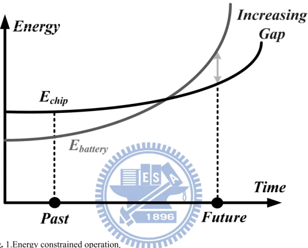
Fig. 1.Energy constrained operation. ... 2
Fig. 2. Power management system diagram of cell phone. ... 3
Fig. 3. The basic structure of linear regulator... 5
Fig. 4. The basic structure of charge pump. ... 6
Fig. 5. The basic structure of boost type voltage mode switching regulator. ... 8
Fig. 6. The CSC technique can (a) reduce the switching power loss and thus (b) improve the power conversion efficiency. ... 11
Fig. 7. The Hysteresis Current Ripple Regulator. ... 12
Fig. 8. The Synthetic Current Ripple Regulator. ... 12
Fig. 9. The synthetic waveform is limited with the hysteresis window defined by the synthetic ripple control. ... 14
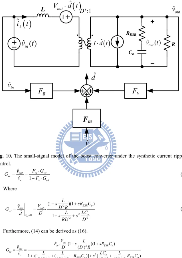
Fig. 10. The small-signal model of the boost converter under the synthetic current ripple control. ... 17
Fig. 11. The synthetic waveform is limited with the hysteresis window defined by the CSC technique. ... 19
Fig. 12. The small-signal model of the boost converter under the CSC technique. ... 21
Fig. 13. The simplified feedback system of the CSC technique. ... 24
Fig. 14. The compensated loop gain T(s). ... 24
Fig. 15. The proposed architecture. ... 26
Fig. 16. The CSC technique force the system operates in (a) the CCM operation at heavy loads and (b) the DCM operation at light loads for power saving. ... 28
Fig. 17. Output energy detect mechanism for switching frequency modulation. ... 28
Fig. 18. The transient response waveform of CSC technique. ... 30
Fig. 19. The schematic of current sensor. ... 31
Fig. 20. The fixed hysteretic current window circuit. ... 32
Fig. 21. The proposed SCG circuit in the CSC technique. ... 36
Fig. 22. Schematic of different In-Out subtractor input stages. (a) Voltage follower. (b) Folded voltage follower. (c) Folded flipped voltage follower. ... 36
Fig. 23. (a) The proposed ZCD circuit. (b) The timing diagram. ... 37
vii
Fig. 25. Waveforms in conventional boost converter with hysteresis control when load current
changes from 70mA to 270mA within 2μs. ... 41
Fig. 26. Transition state waveform. ... 42
Fig. 27. Waveforms in the proposed boost converter with the CSC technique (a) when load
current changes from 200mA to 400mA within 2μs and (b) when load current changes from 400mA to 200mA within 2μs. ... 43
viii
Table Captions
Table I. COMPARISONSOFDIFFERENTTYPEREGULATORS ... 8 Table II. THE PARAMETERS OF SMALL SIGNAL MODEL OF SYNTHETIC CURRENT
RIPPLE CONTROL ... 18
Table III. THE PARAMETERS OF SMALL SIGNAL MODEL OF PROPOSED CSC
TECHNIQUE ... 20
Table IV.THEDESIGNSPECIFICATION ... 39 Table V. COMPARED WAVEFORMS ... 43
1
Chapter 1
Introduction
Portable electronics products such as cellular phones, laptops and diverse multimedia equipments use battery as the main power source. To extend battery life, portable devices stay in sleep mode with a very low static current but require a fast wake-up to reach the normal mode with a much higher operational current. Therefore, the suitable converter for the portable devices needs fast transient response from the standby mode to the normal mode operation while high efficiency is guaranteed over a wide range. In this chapter, we will show the background and basic knowledge of power management system in chapter 1.1 firstly. The classification of power management circuits which including switching converters, linear regulators, and charge pump converters will show in chapter 1.2. The motivation will give in chapter 1.3. Finally, the thesis organization will show in chapter 1.4.
1.1 Background of Power Management
System
With recent advances in integrated mixed-signal circuits and an increasing demand for low-power multifunction system-on-a-chip (SOC) and extended battery runtime, there is a strong need for the development of efficient on-chip power regulation and distribution. As shown in Fig. 1, the growing of battery energy is not enough to supplying power of chips in the future. That is to say, as increasing chip functionality and complexity will overrun available battery energy budget. To solve this problem, the straightforward method is increasing the quantity of power source. Unfortunately, it is not permitted for portable devices
2
because of convenience. In order to decrease the expenses, the power management systems are utilized to provide the specific regulated voltages without consuming unnecessary batteries.
Fig. 1.Energy constrained operation.
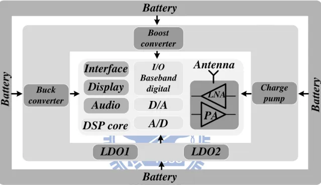
As mention before, the best method of power saving and efficiency increasing is constructs power management system. The advantage of power management system not only generate regulated supply voltage for different specific integration circuits but also suppress the noise which is coupling from battery to electronic devices to extend battery’s lifetime. Take cell phone for example, the basic power management system diagram of cell phone is shown in Fig. 2 [1], a mobile phone may need at least five regulated voltages, one buck converter for DSP core CPU, high PSRR LDO regulators for RF power amplifier and low noise amplifier, one boost converter for color LCD panel, LDO regulators for analog base-band, audio and interface applications, and one charge pump for white light LED driver. The system of cell phone will operate in different modes, such as sleeping mode,
3
communication mode and so on. The control unit is needed to control the internal power management block enable or disable, respectively. That is to say, by using control unit can enhance system efficiency of power supply circuits, such as linear regulators, switching regulators and charge pumps. The ability of saving power and efficiency increasing, that is why power management system playing an important roles in the field of electronics, especially for portable devices.
Boost converter Charge pump
Display
Audio
Interface
DSP core
I/O Baseband digital Buck converterD/A
A/D
LDO1
LDO2
PA
LNAAntenna
Battery
Battery
Fig. 2. Power management system diagram of cell phone.
1.2 Classification of Voltage Regulators
In this section, three kinds of voltage regulators will be introduced briefly, including linear regulators, switched capacitor circuits and switching regulators. Finally, a brief comparison will be given about three types of voltage regulators. The comparisons included circuit complexity, cost, efficiency, load ability and so on.
1.2.1 Linear Regulator
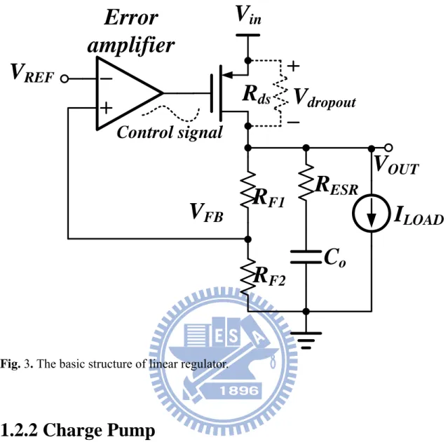
4
(LDO) voltage regulator because there is a drop out voltage (Vdropout ) between input and
output pin about 100~500mV. The power MOSFET has equivalent resistor (RDS) from input
to output, so the power MOSFET size should be well designed to fit the regulated output voltage and load ability. The linear regulator main control circuit was error amplifier, it could adopt output voltage information form resistive feedback network (VFB) then compare to
reference voltage (VREF). After error amplifier operation, it could immediately adjust input
and output difference then control the gate of power MOSFET to supply load current.
The features of linear regulator are described as follows. Firstly, the linear regulator whole circuit is simple and compact, so the die size is smaller than other voltage regulators. And secondly, linear regulator is easy to use, instead of using inductor to transfer energy, the linear regulator just adding two capacitors at input and output pin respectively. As a result, it not only can reduces Printed-circuit board (PCB) area but also cost down. Thirdly, linear regulator only uses resistive feedback network and error amplifier output analogy signal to control power MOSFET, it doesn’t use any switching base circuits. So this kind of regulator has no Electro Magnetic Interference (EMI) and no output ripple, there are very suit for audio, analog and RF circuit applications. Finally, because of without dual storage components, the linear regulator only can do buck regulation. The efficiency is proportional to output voltage and the highest efficiency occurs that output voltage is near to input voltage.
5
VOUT
Co
R
F1
RF2
V
REF
V
in
Vdropout
R
ds
Control signal
Error
amplifier
VFB
RESR
ILOAD
Fig. 3. The basic structure of linear regulator.
1.2.2 Charge Pump
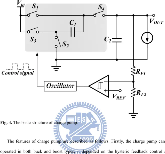
The basic structure of two-phase charge pump regulator is shown in Fig. 4 [3] [4]. Power stage consists of capacitors (C1 C2) and switches (S1 S2 S3 S4). Detailed operation is described
as follows, during the first phase, switches S1 and S2 turn on and switches S3 and S4. The input
voltage charges capacitor C1 to the input voltage level (VIN). Than during the second phase,
switches S3 and S4 turn on and switches S1 and S2. Because the capacitor C1 still maintained
the charge from the previous phase, the output voltage equals to input voltage adding voltage across the capacitor C1, ideally obtains twice input voltage. Adding hysteric feedback control,
6
Fig. 4. The basic structure of charge pump.
The features of charge pump are described as follows. Firstly, the charge pump can be operated in both buck and boost types, it depended on the hysteric feedback control and reference voltage, but it’s more efficiently at boost type. Secondly, the circuit complexity of charge pump is between linear regulator and switching regulator, which is more compact than switching regulator but more complicated than switching regulator. Thirdly, due to digital rail-to-rail switching clock control, the charge pump suffers from EMI and output noise problems. But this problem doesn’t heavier than switching regulator because of lower operation frequency. Finally, the load ability of charge pump is weak because the ability depends on the output capacitor C2 and switching frequency. That is to say, the larger output
capacitor causes the powerful load ability. Because of light load ability typically, the charge pump is very suit for displaying applications, such as driving the gate of MOSFET to on or off.
7
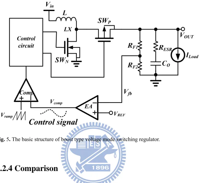
1.2.3 Switching Regulator
The basic structure of boost type voltage mode switching regulator is shown in Fig. 5 [5]. The power stage of switching regulator consists of a couple of complementary power MOSFET (SWP SWN), passive storage elements inductor (L) and capacitor (Co) and resistive
feedback network (RF1 RF2). Detailed operation is described as follows; the resistors RF1 and RF2 sensing the variation of output voltage and error amplifier receives the voltage variation
information then brings the error signal (Vcomp). The comparator’s inputs receive the error
signal from error amplifier and the ramp signal (VRAMP) from ramp generator, then compares
the quantity between the error signal and the ramp signal to decide the duty cycle. After generating the control signal, the PWM generator control the detail timing to avoid short through current. At last, the purposes of gate drivers are driving huge complementary power MOSFET. At the first subinterval, upper power MOSFET (SWP) turns off and lower power
MOSFET (SWN) turns on then input voltage source charge the inductor. At the second
subinterval, lower power MOSFET (SWN) turns off and upper power MOSFET (SWP) turns
on then the inductor will discharge to the capacitor and load. By the above-mentioned, the switching regulator adjusts the output voltage error and regulates to correct voltage.
8
Fig. 5. The basic structure of boost type voltage mode switching regulator.
1.2.4 Comparison
As the above description, three types of voltage regulator have its own advantages and disadvantages. How to choose the best voltage regulator as power supply depend on the electronic applications characteristics and specifications. The comparison of different type voltage regulator is listed in Table I.
Table I. COMPARISONSOFDIFFERENTTYPEREGULATORS
Characteristics Linear Regulator Switching Regulator Charge Pump
Regulation Type Buck Buck/boost/buck-boost Buck/boost
Chip Area Compact Large Moderate
Efficiency Minimum Maximum Medium
9
1.3 Motivation
Basically, the hysteresis control, which contains current-mode and voltage-mode controls, can meet the requirement since hysteresis control is self-stabilized and doesn’t need any compensator if the equivalent series resistance (ESR) of output capacitor is large enough.
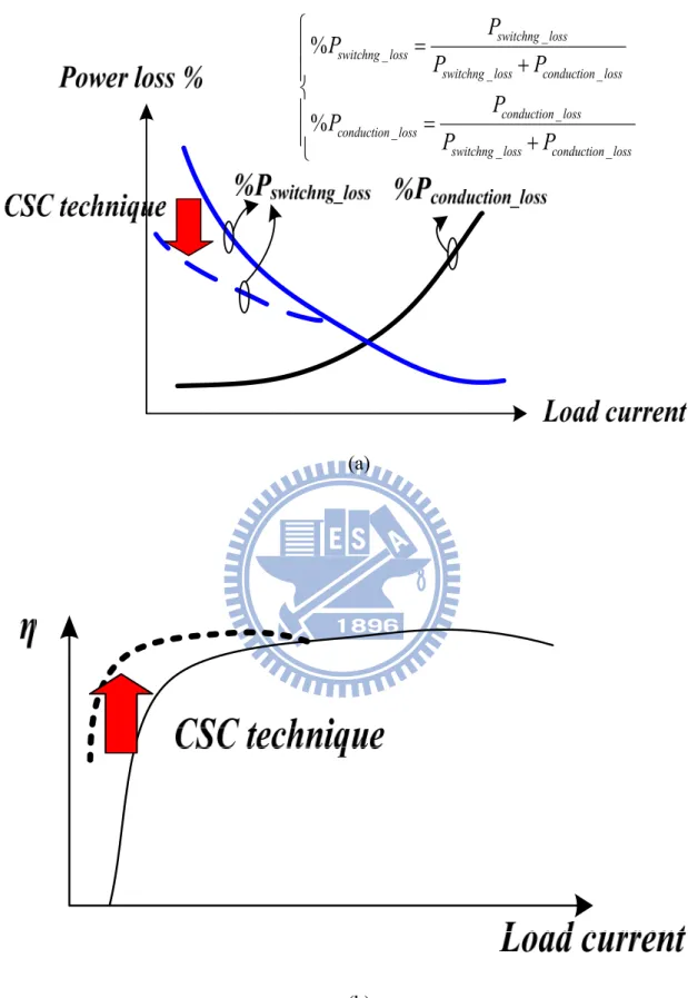
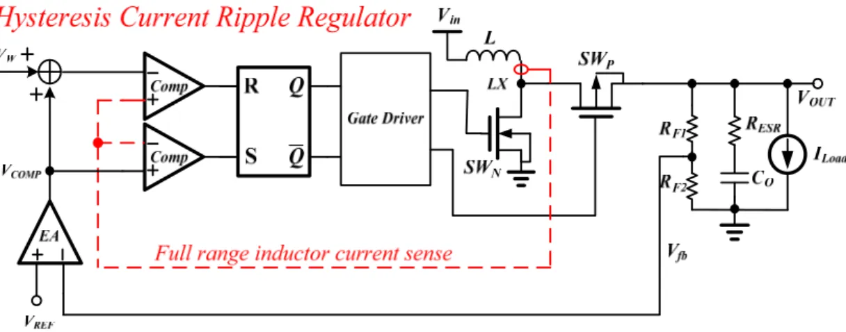
Current-mode and voltage-mode hysteresis controls have the advantages of simple structure and fast transient response. However, both controls have the accuracy problem owing to the lack of error amplifier. Besides, the current-mode control with fast line transient response has low noise immunity and worse load regulation owing to inductor current sensing and the lack of voltage loop, respectively, compared to the voltage-mode control. For example, the hysteresis current ripple regulator as depicted in Fig. 7 has low noise immunity because of the full range inductor current sense. The noise immunity can be improved by the synthetic-ripple modulator (SRM) technique [6] as depicted in Fig. 8 to generate a noise-free ripple signal. However, the SRM control system still contains two poles and thus has a complex compensation network.
Therefore, this paper presents a current-mode synthetic control (CSC) technique to include the current information to decide the charging time of the inductor current. Besides, the CSC technique contains the synthetic clock generator (SCG) to decide the switching frequency. The SCG circuit can maintain a constant switching frequency for the normal operation of the portable devices. On the other hand, in the standby mode, the SCG circuit can prolong the switching period to reduce the switching power loss. The high driving capability and high accuracy due to the usage of error amplifier can be ensured in the proposed CSC
Load ability Medium Maximum Minimum
Complexity Simplest Complicated Medium
10
technique. The performance is similar to the operation in current-mode pulse width modulation (PWM). At light loads, the decreasing switching frequency can effectively improve the power conversion efficiency. However, in the current-mode PWM control, the operation enters the discontinuous conduction mode (DCM) with a constant switching frequency. The switching power loss is still large. The prior arts provide multiple operation modes to achieve high efficiency over a wide load range [7]. Some literatures use the pulse frequency modulation (PFM) to reduce the switching frequency. But the optimum transition between PWM and PFM becomes another serious problem for high power conversion efficiency. Circuit complexity and power conversion efficiency need to be considered at the same in the design of high switching converters. Thus, the proposed CSC technique can reduce the switching frequency with the decreasing load condition. The CSC technique can smoothly change the variable switching frequency at light loads to the constant switching frequency at heavy loads without any complex circuit implementation. Different to the multiple operation modes, the transition point between the nearly constant switching frequency and the adjusted switching frequency is decided by the occurrence of zero inductor current. As depicted in Fig. 6, the switching power loss can be reduced and thus the power conversion efficiency can be greatly improved to maintain high efficiency over a wide load range.
11 _ _ _ _ _ _ _ _
%
%
switchng loss switchng lossswitchng loss conduction loss conduction loss conduction loss
switchng loss conduction loss
P
P
P
P
P
P
P
P
(a) (b)Fig. 6. The CSC technique can (a) reduce the switching power loss and thus (b) improve the
12
Fig. 7. The Hysteresis Current Ripple Regulator.
Fig. 8. The Synthetic Current Ripple Regulator.
1.4 Organization
The organization of this paper is as follows. Chapter 2 shows the small-signal analysis of the synthetic ripple control and improved CSC technique to propose the compensation method to ensure the system stability. Chapter 3 describes the operation of the proposed CSC technique. The internal overall circuit implementation and simulation results are shown in Chapter 4. Experimental results are shown in Chapter 5 to prove the performance and correctness of the proposed MHCC technique. Finally, a conclusion is made in Chapter 6.
13
Chapter 2
The Small-Signal Analysis and
Compensation in CSC Technique
In the chapter 2, the topologies and principle of synthetic current ripple control and improved CSC technique presented. In section 2.1, the basic operation and disadvantage of Synthetic Current Ripple Regulator is introduced. In section 2.2, the small signal modeling of the traditional synthetic ripple control is introduced including. In section 2.3, the small signal modeling of the CSC technique modified is introduced including. The closed-loop with the PI compensation is introduced in the section 2.4.
2.1 Basic operation and disadvantage of
Synthetic Current Ripple Regulator
As depicted in Fig. 8, the synthetic signal generator is used to generate synthetic signal for emulating inductor current ripple. The transduction, gm, is used to transfer inductor voltage to
current flow through capacitor, Cr. As a result, the inductor voltage is integrated then inductor
current ripple is formed. Obviously, the DC level of inductor current is not involved in Vs. In
other word, the path through transduction and Cr is not a current loop in the system. As a
result, the system is still a voltage mode that has to be compensated by type III compensator. It will cause the huge area occupied by output component that we do not like to see. In section 2.3, a current path will be added to improve the compensate method, and the small signal modeling of synthetic current ripple regulator and current mode synthetic control will be
14 showed in next two sections.
2.2 Small Signal Modeling of the synthetic
current ripple control
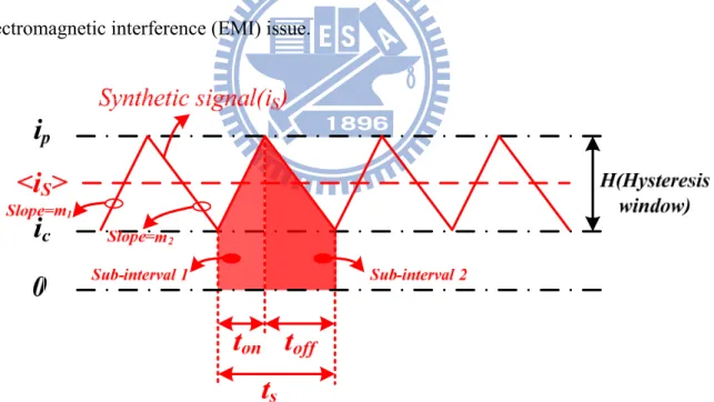
As depicted in Fig. 9, the synthetic current ripple control generate synthetic signal, iS, and
limits it within a hysteresis window, which defines the upper and lower current bands. The synthetic signal rises to reach the upper band of hysteresis window when the high-side MOSFET turns on during ton period [8]. On the other hand, the synthetic signal falls to reach
the lower band of hysteresis window when the low-side MOSFET turns on during toff period.
This synthetic current ripple control is simple and has fast dynamic characteristics except for electromagnetic interference (EMI) issue.
Fig. 9. The synthetic waveform is limited with the hysteresis window defined by the synthetic
ripple control.
The switching period ts as expressed in (1) is equal to the summation of on-time ton and
off-time toff in the CCM operation. The value of toff can be written as (2) according to the
15 s on off
t
t
t
(1)
off out inL H
t
v
v
(2)Considering the small signal analysis, the value of each variable can be written as the summation of the DC term and its perturbation as shown in (3) and (4).
' ˆ ˆ ( ˆ) ˆ ˆ (1 )( ˆ) s s on on s s on on s s T t T t D T t T t D d T t (3) ˆ ( ) ˆ ˆ ( ) off off out out in in L H T t V v V v (4) Keeping the first-order ac terms, the small-signal equations of (3) and (4) can be derived in (5) and (6). ˆ ˆ ˆ on s s t Dt d T (5) 2 ˆ ˆ ( ) (ˆ ˆ ) ˆ ( )
off out in out in off out in out in T v v H L v v t V V V V (6) Similarly, (1) can be written as the summation of the DC term and its perturbation, and keeping the first-order ac terms as shown in (7).
ˆs ˆon ˆoff
t t t (7) Using (6), (7) can be derived in (8).
2 ˆ ˆ ( ) ˆ ˆ ( ) out in s on out in H L v v t t V V (8) Similarly, the peak inductor current, ip, can be expressed as (9) by ton and the average
synthetic signal <iS>.
2
in p S onv
i
i
t
L
(9) (9) can be written as the summation of the DC term and its perturbation, and keeping the first-order ac terms as shown in (10).
ˆ
ˆ
ˆ
ˆ
2
in on on in p SV t
T v
i
i
L
(10)16 (10) can be derived in (11). 2 ˆ ˆ ˆ ( ) on ˆ on P s in in in T L t i i v V V (11) Using (5), (8) and (11), the small-signal duty cycle is derived as (12).
1 2 2 ˆ ' ˆ ˆ on ˆ ˆ ˆ p S in out in s in in out in L T L H D d D i i v v v T V V V V (12)(12) can be simplified as (13) through the use of the DC equivalent equations by assuming
ˆ
S
i
andi
ˆ
p have same perturbation degree.ˆ ˆ ˆ ˆ m C g in v out d F v F v F v (13) 2 ' 1 ' , , and m g v out out K D D D F F F H V V (14)
As a result, the small-signal model of the boost converter with the synthetic current ripple control is illustrated in Fig. 5 and the control-to-output transfer function is shown in (15). R is the output impedance. K is the coefficient constant between vC and iC. RESR is the equivalent
17
ˆ
cv
ˆ
outv
ˆ
d
ˆ
inv
Li t
ˆ
outV
d t
':1
D
ˆ
I d t
Co Rˆ ( )
inv t
L
ˆ ( )
outv
t
RESRF
gF
mF
vFig. 10. The small-signal model of the boost converter under the synthetic current ripple
control. ˆ ˆ 1 out m vd vc c v vd v F G G v F G (15) Where '2 ' 2 ˆ 0 '2 '2 (1 )(1 ) ˆ ˆ 1 in ESR o out out vd o v L s sR C v V D R G LC L D d s s RD D (16)
Furthermore, (14) can be derived as (16).
' ' 2 2 ' 2 ' 2 ' 2 ' 2 0 ( ) ( ) 2 2 0 0 . (1 )(1 ) ˆ ( ) ˆ 1 [ ( )] ( ) ( ) ( ) ( ) ( ) (1 )(1 ) 2 1 out m ESR o out vc o c ESR o ESR o vc z RHP z ESR V L F s sR C v D D R G LC L L L v s R C s R C R D D R D D R s s G s s (17)
18
It is obvious to find that the system contains two complex pole, and two zeros, which include one RHP zero, and one LHP zero. The parameters of small signal model are showed in Table II. The frequency response of the synthetic current ripple control is similar to that of the voltage-mode PWM technique [9]. In other words, the type III compensation must be used for the stability of the system.
Table II. THE PARAMETERS OF SMALL SIGNAL MODEL OF SYNTHETIC CURRENT RIPPLE CONTROL
Fm Fg Fv Gvc0 ωz(RHP) ωz(ESR) ωp1(double pole)
2
K D D
'
H
1
outV
'
outD
V
. ' out m V F D ' 2 ( )D R L 1 ESR o R C 2 2 0 0 0 0 2 0 2 2 4 ( ) 1 2( ) 2.2 Small Signal Modeling of the proposed
CSC technique
As depicted in Fig. 11, the CSC technique generate synthetic signal, ir and limits it within
a hysteresis window, which defines the upper and lower current bands. The synthetic signal rises to reach the upper band of hysteresis window quickly. On the other hand, the synthetic signal falls to reach the lower band of hysteresis window with the slope as same as the inductor discharge slope.
19
Fig. 11. The synthetic waveform is limited with the hysteresis window defined by the CSC
technique.
As same as the analysis in section 2.1, the value of toff can be written as (18).
( ) off on out in L H t t v v (18) ˆ ˆ ( ) ˆ ˆ ( ) off off on on out out in in L H T t T t V v V v (19) (18) can be written as the summation of the DC term and its perturbation as shown in (19). Keeping the first-order ac terms, the small-signal equations can be derived in (20).
2
ˆ ˆ
( ) (ˆ ˆ )
ˆ ˆ ˆ
( )
off out in out in
off on on out in out in T v v H L v v t t t V V V V (20) Similarly, ˆt and s
t
ˆ
onare expressed in (21) and (22).2 ˆ ˆ ( ) ˆ ( ) out in s out in H L v v t V V (21) 2 ˆ ˆ ˆ ( ) on ˆ on P L in in in T L t i i v V V (22) Using (5), (21) and (22), the small-signal duty cycle is derived as (23).
1 2 ˆ ˆ 2 ( ) ˆ ( (ˆ ˆ) ˆ ) ( ) out in on out in P L in s in in out in V V L T H L v v d i i v D T H L V V V V (23)(23) can be simplified as (24) through the use of the DC equivalent equations.
ˆ m (ˆC i ˆL) v outˆ g inˆ
20 ' ' 2 1 1 , , and m g v i out out D F F F H D R DV V (25)
As a result, the small-signal model of the boost converter with the CSC technique is illustrated in Fig. 12 and the control-to-output transfer function is shown in (26). R is the output impedance. Ri is the current sensing gain. RESR is the equivalent series resistance of
output capacitor, Co. ˆ ˆ 1 out m vd vc c v vd m id i v F G G v F G F G R (26) Because of F G Rm id i 1 F Gv vd, we can get
' ' 2 0 ( ) ( ) 1 (1 )(1 ) ˆ 1 ( ) ˆ 2 (1 ) 2 (1 )(1 ) 1 ESR o out m vd vd vc o C m id i i id i vc z RHP z ESR p L s sR C v F G G D R D R G RC v F G R R G R s s s G s (27)
It is obvious to find that the system contains one dominate pole only, and two zeros, which include one RHP zero, and one LHP zero. The parameters of small signal model are showed in Table III. The frequency response of the CSC technique is similar to that of the current-mode PWM technique [10]. In other words, the PI compensation is suitable and easily implemented on the chip [11]. Besides, the advantage of the proposed CSC technique is the remove of the slope compensation in the conventional current-mode PWM control. That is, the proposed CSC technique simplifies the compensation and improves the power conversion efficiency at light loads due to the load-dependent switching frequency. It is more suitable for portable devices.
Table III. THE PARAMETERS OF SMALL SIGNAL MODEL OF PROPOSED CSC TECHNIQUE
Fm Fg Fv Gvc0 ωz(RHP) ωz(ESR) ωp1(single
21 '
2
iD
H D R
'1
outDV
1
outV
' 2 i D R R ' 2 ( )D R L 1 ESR o R C 2 o RC vF
gF
Cv
i
L outv
ˆ
d
inv
Li t
ˆ
outV d t
':1
D
ˆ
Id t
ˆ ( )
inv t
ˆ ( )
outv
t
mF
Fig. 12. The small-signal model of the boost converter under the CSC technique.
2.3 The loop gain analysis with PI
compensator for stability of the system
A closed-loop diagram of the boost converter with the CSC technique is shown in Fig. 13. The loop gain is T(s) as shown in (28).
is the sensor gain, which is equal to22
error amplifier and a proportional-integral (PI) compensator. The PI compensator contributes one low-frequency pole-zero pair, (ωpc, ωz).
( ) vc( ) c( )
T s
G s G s (28) By way of the PI compensator, the original dominate pole of the system will be replace byωpc, and original dominate pole will be cancelled by ωz. As a result, the Gain-Bandwidth of the
system will be expanded. Simultaneously, the DC gain of the system will be enlarged to enhance the load regulation of the system because of the high gain of the error amplifier. The bode plot of the system with compensator, original system, and compensated system are showed in Fig. 14. Where
1 1 p o f R C (29) ' 2 ( ) ( ) 2 z RHP D R f L (30) ( ) 1 2 z ESR ESR o f R C (31) The structure of PI compensator is shown in Fig. 13. It is composed of a transduction, gm,
the output impedance of the transduction, Ro, a resistance, Rz, and a capacitance, Cc.
The relationship between gm, Ro, Rz, Cc, ωpc, andωz are showed below.
1 2 pc o c f R C (32) 1 2 z z c f R C (33)
23
ˆ ( )
out
v
s
ˆ ( )
cv s
ˆ ( )
ev s
ˆ ( )
cv s
24
Fig. 13. The simplified feedback system of the CSC technique.
z
f
pcf
1 pf
25
Chapter 3
The Proposed CSC Technique
Fig. 15 shows the architecture of proposed current-mode hysteresis DC-DC boost
converter with the CSC technique. The synthetic signal Vclk is used to decide the time to store
energy in the inductor. The adjustment of the synthetic clock signal can improve the power conversion efficiency according to the load current condition. On the other hand, the energy stored in the inductor begins to release to the output load when the current sensing signal
Vsense is larger than the hysteresis upper bound, VH. The Vsense signal provides a current path as
dash line showed in Fig. 12 to convert traditional synthetic current ripple control with voltage mode to current mode. As a result, the input current information can be used to control the converter to behave as a constant current source. The dynamics of the inductor is pushed to high frequencies. The system order becomes one to reduce the complexity of compensator. Therefore, the proposed CSC technique can use the proportional-integral (PI) compensation method. In additional, due to the separate of Vramp and Vsense, the low noise immunity problem
26 D ead-time & Driver ZC D
Fig. 15. The proposed architecture.
3.1 The proposed current-mode synthetic
waveform
During the sub-interval II of the inductor current as depicted in Fig. 16(a), the inductor current slope is shown in (34), which can be synthesized by the two signals, Vin and Vout, to
decide the synthetic signal, Vclk, in the CCM operation.
/
in out
V V L (34)
The current-mode hysteresis window is composed of the upper bound VH and the lower
bound VL. The value of VL is equal to the output, Vcomp, of the error amplifier in order to
improve the load regulation performance since worse load regulation in conventional current-mode hysteresis control comes from its lack of voltage regulation loop. Thus, the definition of ‘VL= Vcomp’ can improve the load regulation.
The hysteresis window of the proposed current-mode control is designed as Vw, which is a
27
H L w comp w
V V V V V (35)
(a)
28
Fig. 16. The CSC technique force the system operates in (a) the CCM operation at heavy
loads and (b) the DCM operation at light loads for power saving.
Fig. 17. Output energy detect mechanism for switching frequency modulation.
3.2 Modulation method at different loads
At heavy loads, the system operates in the continuous conduction mode (CCM). Thus, the system switching frequency is dependent on the hysteresis window Vw. As illustrated in Fig. 16(a), the advantage is the switching frequency is a constant value in the CCM operation for
high driving capability.
On the other hand, the system operates in the discontinuous conduction mode (DCM) at light loads. As depicted in Fig. 16(b), in the DCM operation, the synthetic current-mode waveform Vramp, is kept constant once the inductor current becomes zero, which is detected by
the zero current detector (ZCD) in Fig. 15. Owing to the constant Vramp if the signal ZC is
equal to one, the off-time period is extended. Simultaneously, the output capacitor can’t gain energy and the output of error amplifier Vcomp increases to be higher than Vramp, again. The
output energy detect mechanism is shown in Fig. 17. The speed of Vcomp increasing higher
than Vramp is dependent on the load condition. When load current becomes light, the speed of
Vcomp increases quicker than even light load current. Then Vcomp takes shorter to hit Vramp to
initial the next period. As a result, the switching frequency increases with the frequency of
Vramp increasing. The switching frequency is reduced in the DCM operation to save much
switching power loss at light loads. In other words, the switching frequency, which depends on the value of load current, causes the switching power loss is inversely proportional to the switching frequency. That is, the variable switching frequency in the DCM operation can
29
reduce the switching loss and thus improve the power conversion efficiency at light loads.
3.3 Modulation method at transient
response
Furthermore, the new CSC technique has fast transient response since the trailing and
leading edges can rapidly react to the output load variation. As shown in Fig.18 , the on time of the pulse width signal adaptively increases or decreases when the load current suddenly increases or decreases, respectively. Similarly, the off time can be modulated to improve the transient response time due to the CSC window controlled by the error amplifier.
30
Fig. 18. The transient response waveform of CSC technique.
Chapter 4
The Circuit Implementation
The CSC technique in Fig. 15 contains two parts. The first part is the insertion of current information, which is implemented by the comparison of the low-side NMOSFET current sensing signal Vsense with the upper bound signal VH. The second part as depicted in Fig. 21
is the synthetic clock generator (SCG). The SCG circuit can ensure the switching frequency nearly constant if the converter operates in the CCM operation. On the other hand, the SCG circuit can adjust the switching frequency to reduce the switching power loss at light loads if the converter operates in the DCM operation. In brief, constant switching frequency ensure low electromagnetic interference (EMI) and high driving capability at heavy loads while the decreasing switching frequency can improve the power conversion efficiency at light loads.
4.1 Current Sensor
The CSC technique needs to sense the charging interval of inductor current. Thus, an accurate current sensor is required. As depicted in Fig. 19, the transistors M1 and M2 are
biased by the same current IB. Thus, VGS1=VGS2. When the inductor current charges, the
PowerNMOS turn on with the signal, Ng, pull high. At the same time, MS3, MS4 turn on to
make PowerNMOS and MS3 form a current mirror pair with
3 : :1 S PowerMOS M W W N L L . And M2, M3 form a negative feedback to make sure source nodes of M1, M2 tight to Vx for
accuracy of current mirror. Finally, ( L B)
B sense
I I
I I
N
. When IB is small, L sense
I I
31
the other hand, PowerNMOS turn off with the signal, Ng, pull low, MS1, MS2 turn on to provide
IB paths to flow for reducing react time. The current sensing gain, Ri, can be derived in (36).
sense i R R N (36)
Fig. 19. The schematic of current sensor.
4.2 Fixed Hysteretic Current Window
Circuit
In Fig. 20, the fixed hysteretic current window circuit is designed to accurately control the output ripple for ensuring the regulation performance. The low band of the fixed hysteretic current window is controlled by the output of the error amplifier, which is Vcomp. Thus, a
unity-gain buffer used to filter out the switching noise can generate the low band VL. The
32
IR-drop is derived by a constant current flowing through a hysteresis resistor Rw. As a result,
the upper band VH can be expressed by (37).
H L w w V V I R (37)
V
comp(V
L)
R
wV
HV
LV
wUnity-gain buffer
V
HV
LV
wVDD
I
wFig. 20. The fixed hysteretic current window circuit.
4.3 The synthetic clock generator (SCG)
As the SCG circuit depicted in Fig. 21, in the beginning of the switching period, a current
Ic introduced by the transistor M4 flows into the capacitor Cramp to ramp up the signal Vramp.
Vramp is rapidly charged to be higher than VH since Ic is much higher than Id. Thus, the output
of the SR-latch is triggered from high to low to turn on switch M6. The discharging period of
the inductor current is emulated by the discharging current Id to generate the synthetic clock.
33
difference of the input and output voltages [12]. The discharging current, Id can be expressed
as (38). The input stage of in-out subtractor is voltage follower, as shown in Fig. 22. In Fig.
22(a), the output impedance of original voltage follower is shown as (40). To reduce the
output impedance and improves the in-out subtractor linearity, the folded voltage follower is implemented, as illustrated in Fig. 22(b). This structure can reduce output impedance effectively and the output impedance is shown in (41). But the main disadvantage is input swing depends on the threshold voltage, it becomes very small in modern CMOS technology. The input swing can be written as (43). For a wider input swing range, the folded flipped voltage follower is implemented, as illustrated in Fig. 22(c). This structure not only reduces output impedance but also improves the input swing range. The output impedance of the folded flipped voltage follower and the input swing range is shown in (42) and (44) respectively. By using the folded flipped voltage follower as in-out subtractor input stage, the output impedance on the node N1 and node N2 in Fig. 21 is greatly reduced, and the linearity
of in-out subtractor approaches to ideal value.
2 2 fb inFF 2 out in d ERROR gm gm V V V V I I R R (38) 2 1 2 where = F and inFF in F F R V V R R (39) And then, the signal Vramp begins to ramp off and compare with the lower bound VL to
decide the next switching period. The slope of the discharging period is proportional the negative inductor current slope. Once the value of Vramp is lower than that of VL, the switch M6
is turned off to ramp up the Vramp, again. The signal Vramp is limited with the hysteresis
window, which is defined by VH and VL. In conclusion, the SCG circuit decides the switching
frequency. In the CCM operation, the inductor current will not be smaller than zero. Thus, the switching frequency is basically decided by the hysteresis window. If the value of the input and out voltages is not changed, the switching frequency can be kept constant in the CCM
34 operation.
On the other hand, in the DCM operation, the signal ZC is set to high when the
zero-current detector (ZCD) senses the inductor current is equal to zero. The transistor M1 will
directs the discharging current Id to ground and the signal Vramp is clamped at a constant value.
The switch M7 and Csample are used to balance the DC level of Vramp at different periods in the
DCM operation to ensure the switching period regularity. When ZCD is high, the voltage
Vramp is clamped. At the same time, M7 turns on to connect Csample and Cramp. With the
mechanism, the voltage error of Vramp between two periods will be cancelled with Csample>>
Cramp. And the ‘‘dummy’’ switch M8, M9, driven by ZCD are added to the circuit such that
after M7 turns off and M8, M9 turns on, the channel charge deposited by M7 on Cramp and
Csample is absorbed by M8, M9 to create a channel. In other word, the charge injection effect is
cancelled [11].
As a result, the switching frequency is decreased to reduce the switching power loss as shown in Fig. 16(b). The switching frequency of the boost converter is dependent on the load current.
36
Fig. 21. The proposed SCG circuit in the CSC technique.
M
1V
inV
outI
BI
BM
2M
1V
inV
outI
BM
2V
inV
out2I
BM
1VDD
(a)
(b)
(c)
VDD
VDD
1 1 (40) o m R g 2 1 2 1 1 (41) o m m o R g g r 2 1 2 1 1 (42) o m m o R g g r 1 2 1 2( ) swing ( sat ) ( ) sat (43)
in DSM SG M SG M T T DSM
b V VDD V V VDD V V V V
2 2 1 2 2 1
( ) ( ) ( ) (44)
B B
swing sat sat sat
in DS I SGM GSM T DS I SGM DSM
c V VDD V V V V VDD V V V
Fig. 22. Schematic of different In-Out subtractor input stages. (a) Voltage follower. (b)
Folded voltage follower. (c) Folded flipped voltage follower.
4.4 The zero current detector (ZCD)
The proposed ZCD is illustrated in Fig. 23(a) to control the switching frequency in the SCG circuit. The transistors M1-M3 and M4-M6 construct the level shifters to shift the signals
VX and Vout to the VX1 and Vout1, respectively, to meet the input common-mode range of the
comparator. In the first interval of each switching period, the INP is logic high to keep the Pg
high and reset the D-flip-flop to pull the ZC low. In the second interval of each switching
period, the INP is triggered to logic low to turn on the power PMOSFET if the signal ZC is
still low. Once the reverse inductor current occurs, VX is smaller than Vout corresponding to
VX1 is smaller than Vout1. Simultaneously, the output of the comparator is triggered from low
to high to set the signal ZC high to indicate the zero current condition. The signal Pg is
changed from low to high to turn off the power PMOSFET and avoid the occurrence of the reverse inductor current.
37 (a)
(b)
38
Chapter 5
Whole chip experimental Results
The proposed boost convert with the CSC technique was fabricated by TSMC 0.25 μm CMOS process. The threshold voltages of nMOSFET and pMOSFET are 0.477 V and -0.596 V, respectively. The off-chip inductor and output capacitor are 1 μH and 6.8 μF, respectively. The output voltage Vo is 4.5V. The specification is listed in Table IV. The chip micrograph is
shown in Fig. 24 and the chip area is about 1564 μm × 1813 μm including the test pads.
Test buffer ZCD&Digital control Cs EA Compensator CSC BG BIAS Power Nmos Power Pmos Driver Vx PVSS Vo Avss Avdd Dvss Dvdd
Fig. 24. Chip micrograph.
Fig. 25 shows the output waveforms at different load current condition when the converter operates at the CCM mode and DCM mode. Fig. 25(a) and (b) show that the proposed CSC technique adjusts the switching frequency of the boost converter dynamically according to the load current condition. Fig. 25(c) shows the switching frequency maintain 1.7MHz to enhance
39
system performance when inductor current enter into CCM mode. The relationship between load current, switching frequency and output ripple is listed in Table V. It demonstrates that the switching frequency with different load is almost the same at CCM mode. On the other hand, the switching frequency reduces with the load current decrease at DCM mode.
Fig. 26 demonstrates the waveform at the transition point. It is seamless between PFM and PWM mode, and the overshoot which ordinary pfm mode will occur is also reduced
The waveforms of the output voltage and the inductor current during load transient response are shown in Fig. 27. The settling times are about 26µs and 27µs for Vin = 2.7V and
the change in load current from 200mA to 400mA and from 400mA to 200mA, respectively. It demonstrates the CCM mode operation.
Fig. 28 shows the simulation efficiency of proposed structure. The switching frequency of the boost converter can be effectively reduced at light load. As a result, the efficiency can be kept larger than 90% at load current= 10mA. It demonstrates that the efficiency can be kept high due to the implementation the technique.
Table IV.THEDESIGNSPECIFICATION SPECIFICATIONS
Technology TSMC 0.25μm 1P3M
Chip size 1700μm × 1800μm Supply variation ( VIN ) 2.7V - 4.5V
Output voltage ( VOUT ) 4.5V
Maximum output
loading current 400mA Inductor ( L ) 1μH Output capacitor ( CO ) 6.8μF
40 Equilibrium series resistance of the output capacitor (RESR)
50mΩ Operation temperature 0~100℃ PFM range 0mA - 150mA
41 (b)
I
L
V
out
f
sw=1.67MHz
∆V
out=46mV
∆I
L=660mA
(c)Fig. 1. Waveforms in conventional boost converter with hysteresis control when load current
42
43 (a)
V
OUTI
L 80mV 27usec 200mA 400mA (b)Fig. 26. Waveforms in the proposed boost converter with the CSC technique (a) when load
current changes from 200mA to 400mA within 2μs and (b) when load current changes from 400mA to 200mA within 2μs.
Table V. COMPARED WAVEFORMS
IL fs Vout ripple 4mA 55kHz 34mV 6mA 71kHz 31mV 8mA 97kHz 30mV 10mA 114kHz 31mV 20mA 234kHz 30mV
44 40mA 460kHz 31mV 60mA 714kHz 32mV 80mA 909kHz 31mV 100mA 1.16KHz 34mV 200mA 1.66MHz 37mV 300mA 1.67MHz 46mV 400mA 1.7MHz 50mV
45
Chapter 6
Conclusion
The proposed CSC technique in boost converters can speed up transient response due to the current-mode hysteresis control and improve efficiency over a wide load range. The CSC technique behaves high accuracy similar to the current-mode control without the need of slope compensation for simplicity. The load-dependent switching frequency at light loads results in high power conversion efficiency. Experimental results show that the output voltage ripple can be kept smaller than 50mV over a wide load current range from 0mA to 400mA with power conversion efficiency higher than 90% at load current of 10mA.
6.1 Future Work
The CSC technique also minimizes the external components and thus it has the advantage of small footprint. But the CSC has the same disadvantage of the complex design the EMI filters because of the frequency variation along with the input supply and output voltage. Therefore, the improvement of EMI issue is important in the future.
46
Reference
[1] D. Maksimovic, “Power management model and implementation of power management ICs for next generation wireless applications,” Tutorial presented at the International
Conference on Circuits and System (ISCAS), 2002.
[2] ‘‘Technical Review of Low Dropout Voltage Regulator Operation and Performance,” Texas Instruments Incorporated, Dallas, TX, Aug. 1999.
[3] P. Favrat, P. Deval and M. J. Declercq, ‘‘A high-efficiency CMOS voltage double,”
IEEE Journal of Solid-State Circuits, vol. 33, pp. 410-416, March 1998.
[4] James S. Zeng, Lajos Burgyan, and Rendon A. Hollowa, ‘‘Highly efficient step-down/step-up and step-up/step-down charge pump,” United States Patent, Patent Number 6,657,875, July 16, 2002.
[5] Robert W. Erickson and Dragan Maksimovic, Fundamentals of Power Electronics, 2nd ed., Norwell, MA: Kluwer Academic Publishers, 2001.
[6] G. Jurasek, G. Levin, P. Sisson, and S. Repplinger, “High Efficiency Automotive Power Supply with Hysteretic Current Mode Controller,” in Proceedings of IEEE Applied
Power Electronics Conference and Exposition, vol. 2, pp. 861, March 1996.
[7] Wei Tang, Fred C. Lee, “Small-Signal Modeling of Average Current-Mode Control,”
IEEE Trans. Power Electron., vol. 8, pp. 112-119, Apr. 1993.
[8] R. B. Ridley, “A new, continuous-time model for current-mode control,” IEEE Trans.
Power Electron., vol. 6, pp. 271-280, April 1991.
[9] J. H. Park and B. H. Cho, ”Small Signal Modeling of Hysteretic Current Mode Control Using the PWM Switch Model,” IEEE COMPEL, pp. 225-230, July 2006.
[10] K.D.T. Ngo, S. K. Mishra, and M. Walters, “Synthetic ripple modulator for synchronous buck converter,” IEEE PE Letter, vol. 3, pp.148-151, Dec. 2005.
47
[11] B. Razavi, Design of Analog CMOS Integrated Circuits. Boston, MA:McGraw-Hill, 2001.
[12] Hong-Wei Huang, Wei-Lun Hsieh, and Ke-Horng Chen, “Programmable voltage-to-current converter with linear voltage control resistor,” IEEE International