Field emission from well-aligned carbon nanotips grown in a gated device structure
C. L. Tsai, C. F. Chen, and C. L. LinCitation: Applied Physics Letters 80, 1821 (2002); doi: 10.1063/1.1459109
View online: http://dx.doi.org/10.1063/1.1459109
View Table of Contents: http://scitation.aip.org/content/aip/journal/apl/80/10?ver=pdfcov
Published by the AIP Publishing
Articles you may be interested in
Field emission of aligned grown carbon nanotubes
AIP Conf. Proc. 685, 550 (2003); 10.1063/1.1628091
Fabrication and characterization of gated field emitter arrays with self-aligned carbon nanotubes grown by chemical vapor deposition
Appl. Phys. Lett. 81, 2070 (2002); 10.1063/1.1506408
Field electron emission from individual carbon nanotubes of a vertically aligned array
Appl. Phys. Lett. 81, 343 (2002); 10.1063/1.1489084
Field emission from well-aligned, patterned, carbon nanotube emitters
Appl. Phys. Lett. 76, 1776 (2000); 10.1063/1.126164
Field emission properties of carbon nanotubes
J. Vac. Sci. Technol. B 18, 665 (2000); 10.1116/1.591258
This article is copyrighted as indicated in the article. Reuse of AIP content is subject to the terms at: http://scitation.aip.org/termsconditions. Downloaded to IP: 140.113.38.11 On: Thu, 01 May 2014 06:25:26
Field emission from well-aligned carbon nanotips grown in a gated
device structure
C. L. Tsai,a) C. F. Chen, and C. L. Lin
Department of Materials Science and Engineering, National Chiao Tung University, 1001 Ta Hsueh Road, Hsinchu 30050, Taiwan, Republic of China
共Received 9 November 2001; accepted for publication 11 January 2002兲
Vertically well-aligned, high-aspect-ratio carbon nanotips have been directly grown upward on the gated device structure with 4m gate aperture. The nanotips rapidly nucleate and grow without any catalyst. In addition, selected area deposition of nanotips is achieved by using a Pt layer as inhibitor in the bias-assisted microwave plasma chemical vapor deposition. The field emission current of nanotips on the gated structure is 154A共at a gate-to-cathode voltage of Vgc⫽50 V兲. This results from the following reasons: 共i兲 short gate-tips spacing, 共ii兲 small gate aperture, and 共iii兲 the high-aspect ratio of nanotips. © 2002 American Institute of Physics. 关DOI: 10.1063/1.1459109兴 Up until now, there have been numerous reports on
de-veloping the different designs of field emission displays.1,2 Since the discovery of carbon nanotubes, the application of field emission has attracted much interest.3,4However, cata-lysts 共such as Fe, Co, Ni, etc.兲 are used to promote the growth rate of the nanotubes. Furthermore, the randomly ori-ented nanotubes also need the posttreatment before applica-tions. In this study, well-aligned and high-aspect-ratio nan-otips are directly synthesized in a 4 m gated device structure. The gaseous mixture of CH4/CO2 is used in the bias-assisted microwave plasma vapor deposition. The growth rate of nanotips is higher in highly carbon-concentrated CH4/CO2 gas mixture than in conventional mixtures of hydrocarbons diluted in hydrogen.
A Pt-gated device structure with 50⫻50 circles was ini-tially fabricated by semiconductor process technology. Start-ing substrates were mirror-polished n-type 共100兲 oriented wafers. The width and the depth of each circle were 4 m and 7000 Å, respectively. After the gated device structure was generated, specimens were put in the bias-assisted mi-crowave plasma chemical vapor deposition system to deposit carbon nanotips. Reactive gaseous mixture of CH4– CO2was used in deposition. The flow rates of CH4/CO2and the depo-sition time remained constant at 30/30 sccm and 15 min, respectively. During deposition, the Si substrate was sub-jected to a negative bias voltage.
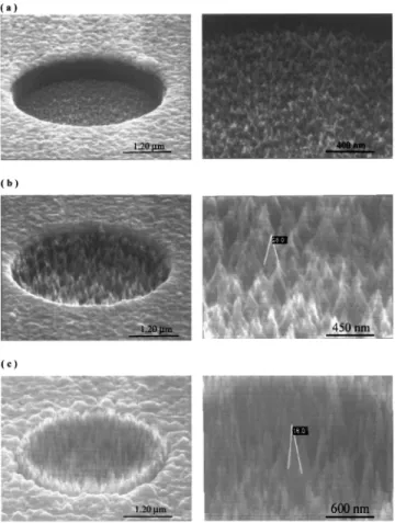
Figure 1 shows scanning electron microscopy 共SEM兲 photographs of carbon nanotips grown under different biases. Each picture is only one of the 50⫻50 circles on the device. On the right-hand side of every picture is an enlarged image. The SEM images indicate that carbon nanotips can be uni-formly grown only inside the Pt-gated device structure in the absence of amorphous carbon (a-C) on the Pt-gated surface. The selective area deposition of nanotips is attributed to the following two reasons. One is that carbon materials are more easily grown on silicon than on the Pt-gated layer because Pt is a highly chemically inert material that does not nucleate carbon materials on an unscratched Pt surface.5,6The other is that electrical field is concentrated on the silicon substrate surface because the n-type silicon conducts electrons, but
electrons can not pass through silicon dioxide 共dielectric layer兲 within a Pt-gated layer. Consequently, the local depo-sition biased effects are all within the silicon substrate. How-ever, increasing the deposition time causes some a-C to form on the Pt-gated surface.
Figures 1共a兲–1共c兲 reveal that applying a bias can en-hance the growth of carbon nanotips in CH4/CO2 gas mix-ture. Thus, the higher bias drastically enhances the growth of carbon nanotips. The bias-assisted effect is also valid for the hydrocarbon diluted in hydrogen.7However, samples grown under a bias more negative than⫺130 V cause the height of the tips to exceed that of the Pt gate. In this situation, the gated device structure becomes a diode structure. By
con-a兲Electronic mail: [email protected] FIG. 1. SEM photographs of nanotips grown under共c兲 ⫺150 V. 共a兲 ⫺100, 共b兲 ⫺130, and
APPLIED PHYSICS LETTERS VOLUME 80, NUMBER 10 11 MARCH 2002
1821
0003-6951/2002/80(10)/1821/2/$19.00 © 2002 American Institute of Physics This article is copyrighted as indicated in the article. Reuse of AIP content is subject to the terms at: http://scitation.aip.org/termsconditions. Downloaded to IP:
trast, a bias less negative than⫺130 V only leads to tiny tips inside the hole. In addition, all the tips grow upward under biased conditions. The tip angle of the nanotips decreases as the bias increases. In other words, a higher bias generates higher density, sharper, and higher-aspect-ratio nanotips. CH4/CO2 can promote the growth rate over that with con-ventional gas mixtures 共hydrocarbons diluted in hydrogen, for example, CH4/H2兲8 because of the high carbon concen-tration in the CH4/CO2 gas mixture.
Figure 2共a兲 displays the transmission electron micros-copy 共TEM兲 images of an end section of an individual nan-otip. The main feature of note is the transmission electron microscopy somewhat irregular shape of the tip with one primary protrusion. The Fourier filtering transformation
共FFT兲 indicates that the end section is a-C. Moreover, Fig.
2共b兲 displays the lateral section of the same tip. It shows microcrystalline graphite on the lateral section. The FFT of
Fig. 2共b兲 also proves the existence of the microcrystalline graphite.
Figure 3 presents Raman spectra of tips grown under various applied biases. The spectra do not obviously differ. All of them have two sharp peaks located on about 1355 cm⫺1and 1582 cm⫺1, respectively. The peaks imply that the nanotips are characteristic of microcrystalline graphite. The Raman spectra of a-C can be decomposed into two features located approximately at 1550 cm⫺1 共corresponding to the G-line associated with the optically allowed E2g zone center mode of crystalline graphite兲 and 1350 cm⫺1 共roughly cor-responding to the D-line associated with disorder-allowed zone-edge modes of graphite兲. The positions, widths, and relative intensities of these two peaks are found to vary sys-tematically with deposition conditions and properties of the tip.9,10The intensity of these two peaks is the same indicat-ing that the samples contain much a-C.
Figure 4 displays the electron-emitting characteristic of the nanotips on gated device structure. The field emission properties are measured by using a triode technique. An an-ode plate, an indium tin oxide glass, is placed above the Pt gate and biased to⫹800 V. A 100m slide glass is used for the spacer. The anode current (IA) is then measured as a function of gate-to-cathode bias voltage in a vacuum of 1
⫻10⫺6 Torr. The gate-to-cathode voltage (V
gc) is varied from 0 to 50 V. The field emission current (Ia) of nanotips on the gated device structure is about 154A共at a gate-to-cathode voltage of Vgc⫽50 V兲. Therefore, the higher emis-sion current of the nanotips results from the following causes: 共i兲 short gate-tips spacing, 共ii兲 small gate aperture, and共iii兲 the high-aspect-ratio of the nanotips.
The authors would like to thank the National Science Council of the Republic of China for financially supporting this research under Contract No. NSC 90-2216-E-009-036.
1
W. Yi, S. Jin, T. Jeong, J. Lee, S. Yu, Y. Choi, and J. M. Kim, Appl. Phys. Lett. 77, 1716共2000兲.
2J. O. Choi, H. S. Jeong, D. G. Pflug, A. I. Akinwande, and H. I. Smith,
Appl. Phys. Lett. 74, 3050共1999兲.
3
Q. H. Wang, A. A. Setlur, J. M. Lauerhass, J. Y. Dai, E. W. Seeling, and R. P. H. Chang, Appl. Phys. Lett. 72, 2912共1998兲.
4N. S. Xu, Z. S. Wu, S. Z. Deng, and J. Chen, J. Vac. Sci. Technol. B 19,
1370共2001兲.
5J. S. Lee, K. S. Liu, and I. N. Lin, Appl. Phys. Lett. 71, 554共1997兲. 6
D. N. Belton and J. Schmeig, J. Appl. Phys. 69, 3032共1991兲.
7S. Yugo, T. Kanai, T. Kimura, and T. Muto, Appl. Phys. Lett. 58, 1036
共1991兲.
8C.-F. Chen and H.-C. Hsieh, Diamond Relat. Mater. 9, 1257共2000兲. 9M. A. Tamor and W. C. Vassell, J. Appl. Phys. 76, 3823共1996兲. 10
J. Wagner, M. Ramsteiner, C. Wild, and P. Koidl, Phys. Rev. B 40, 1817 共1989兲.
FIG. 2. TEM images and Fourier filtering transformation共FFT兲 of 共a兲 the end section and共b兲 lateral section of an individual tip.
FIG. 3. Raman spectra of nanotips growing under different applied biases.
FIG. 4. Emission current versus the gate voltage of nanotips on a gated device structure.
1822 Appl. Phys. Lett., Vol. 80, No. 10, 11 March 2002 Tsai, Chen, and Lin
This article is copyrighted as indicated in the article. Reuse of AIP content is subject to the terms at: http://scitation.aip.org/termsconditions. Downloaded to IP: 140.113.38.11 On: Thu, 01 May 2014 06:25:26