RTUIFR-IS
A 13
1
GHz Push-push VCO in 90-nm CMOS
Technology
Ping-Chen
Huang,
Ren-Chieh Liu, Hong-Yeh
Chang,
Chin-Shen Lin,
Ming-Fong
Lei, Huei
Wang,
Chia-Yi
Su',
and
Chia-Long Chang'
Department of
EIectrical Engineering and Graduate Institute of Communication Engineering,
National
Taiwan University, Taipei, 106,
Taiwan, R. 0. C.
tTaiwan Semiconductor Manufacturing Company, Hsinchu, 300, Taiwan, R.
0. C.
Abstract
-
A 131 GHz crass-coupled push-push voltage controlled oscillator (VCO) is realized in 90nm CMOStechnology. It can be tuned from 129.8 i o 132 GHz, with an estimated phase noise of -108.4 dBc/Hz at 10 MHz offset. The oscillator provides a push-push output power of -15.2 dBm and a fundamental output power of c0.33 dBm, under core current of 20 mA from a 1-V supply voltage. Maximum gush- push and fundamental output powers are -11.4 dBm and +2.1
dBm, respectively. To the authors' knowledge, this is the highest frequency CMOS VCO ever reported.
Index Terms - CMOS, MMIC, millimeter-wave (MMW),
cross-coupled, push-push, voltage-controlled oscillator (VCO), phase noise.
I. INTRODUCTION
There are growing demands in upper millimeter-wave
(MMW) electronics for various applications. The use of frequency bands beyond 100 GHz offers advantages such as smaller antenna and chip sizes. VCO is one of the key components in MMW systems. Integrated VCOs with operating frequencies beyond 100 GHz have been reported in previous literatures [ 11-(51. They were realized using 111-V compound devices [1]-[3] or SiGe HBT
[4]-[5].
Recently, the trend is to advance the CMOS technology from RF into millimeter-wave range to take the advantage
of low production cost and integration with baseband circuits. Many millimeter-wave VCOs were realized in CMOS technology [6]-[ 171. The highest fundamental oscillation frequency ever reported was 100 GHz [ 161, but the output power is low since the oscillation frequency is close to
f-.
To achieve higher oscillation frequency, push-push VCO are reported [SI, [l5], [17]. Although it has been pointed out that differential cross-coupled pair cannot achieve high frequency oscillation due to the maximum attainable oscillation frequency [ 171-[ 1XI,
it has the advantage of obtaining compact circuit size and the ease of design due to the inherently differential fundamental signals.In this paper, we present a CMOS push-push VCO using a cross-coupled pair as the VCO core. The central oscillation fi-equency is 131 GHz and the tuning range is
1.7%. At each of the fundamental frequency differential ports, up to +2.ldBm output power can be obtained. To the authors' knowledge, this push-push VCO demonstrates the highest frequency CMOS VCO to date and provides V-band differential signals, which also have the highest output power compared with previously reported CMOS V-band VCOs. A comparison of recently reported CMOS VCOs is given in Table I.
11. CIRCUIT DESIGN
Push-push principle can be used for MMW VCO design with the advantage of exploiting the higher device gain and passive component and varactor Q-factors available at lower Frequencies [I], Most push-push VCOs are implemented by combining anti-phase balanced structures and extracting the second harmonic signal from the virtual ground where the anti-phase fundamental signals cancel out. Also, the even mode oscillation needs to be suppressed in the design [1]-I4], [17]. In this paper, we employed a cross-coupled pair to implement the push- push VCO, similar to those reported in [SI, [15], and [19].
-
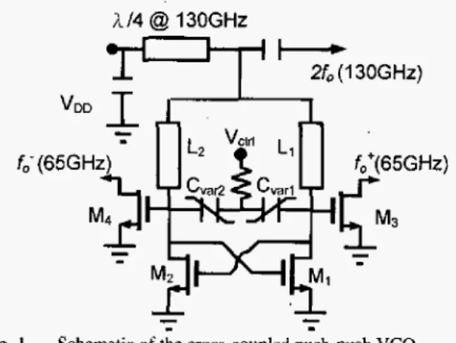
IFig. 1 . Schematic of the cross-coupled push-push VCO.
The circuit schematic is shown in Fig. 1. Transistors M, and M, form the cross-coupled VCO core. The transmission lines, L, and L,, and varactors Cvxl and Cvd
0-7803-8983-2/05/$20.00 0 2005 IEEE
613
serve as the LC tank to determine the fundamental oscillation frequency. M, and
M,
are the output buffers for the differential fundamental signals. The second-harmonic signal is extracted from the center of L, and L,. The supply current is fed through the n4-line at 13 1 GHz to the VCO core.The VCO was fabricated using TSMC's 90nm CMOS technology featuring a single poly layer for the gates of the MOS and nine copper metal layers for inter- connection (1P9M). The device with gate width of 32 pm yields a fT o f 142 CiHz and fmav of 160 GHz at 1-V drain bias. MIM capacitors of lfF/mm2 are available using oxide inter-metal dielectric. Two types o f palysilicon resistors are provided with individual dose
of
ion- implantation.Both the transistors M, and M, are NMOS of 8 fingers with total gate width of 32 pm. The negative resistance of the cross-coupled pair approaches to zero as the frequency approaches to maximum attainable oscillation frequency [ 181. To ensure the oscillation, it is necessary to take into account the variation of the device parameters, i.e., C,,
Cgd, C,,,
R,,
etc., such that the transistors operate in a region where the cross-coupled pair generates enough negative resistance regardless of the process variation. The center fundamental oscillation frequency is designed at65.5 GHz, where the sum of the real parts of the cross- coupled pair and the LC-tank remains negative even if the device parameters vary +40% from the nominal values.
The fine-tuning frequency is determined by the bias of varactors from the node V,,,,. The NMOS varactors are laid out as a multi-finger structure to maximize @factor. In order to avoid the decrease in Q of the transmission line inductors due to the lossy substrate, the transmission lines
are implemented as a coplanar waveguide (CPW) series
with
shunted asymmetric coplanar slots(ACPS) [I
51rather than thin-film microstrip lines. The shunted ACPSs provide the inductances L i and L2, while the CPW is used as the interconnection between the push-push output, L ,
and Lz. The CPW i s designed to have characteristic impedance of 50
fl.
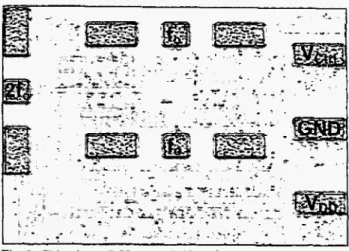
The line width and gap of the CPW is chosen to be 20 and 5 pm, respectively. Each of the ACPS is designed to have an inductance of 0.03 nH, with line width and gap of 5 pm and 15 pm, respectively. Figure 2 shows the chipphoto,
and thechip size
is 0.55m m
x 0.65 mm, including RF testing pads.Fig. 2. Chip photo (0.55 m m x 0.65 mm).
111. MEASUREMENT RESULTS
The chip was measured via on-wafer probing. The VCO starts to oscillate at 20-mA bias current from a I-V supply. The fundamental and second harmonic output ports were measured by two MMW spectrum analyzer systems. A GGB W-band probe, Agilent 11970W harmonic mixer, and E4448A spectrum analyzer were used for harmonic output port. The harmonic mixer features a conversion loss of 43.5 d 3 at 110 GHz. For the fundamental output ports, two GGB V-band probes were used for on-wafer probing. One port was terminated with a
5 0 4
load, and the other port was connected to the V-band spectrum analyzer system which consists of an Agilent 11974V pre- selection harmonic mixer and an 8565EC spectrum analyzer. Waveguide connections were used for connections between harmonic mixers and probes.The output spectrum of the push-push port is shown in Fig. 3. Under core supply current of 20-mA from a I-V supply voltage, the output power at the push-push port measured using a D-band power sensor is -15.2 dBm, while the output power at the fundamental port measured via the V-band spectrum analyzer system is +0.33 dBm. Each buffer consumes 8 mA from 1-V supply. The measured power on the spectrum analyzer is lower than that on the power sensor because of the excessive conversion loss of the harmonic mixer. The maximum push-push and fundamental output power are -1 I .4 dBm
and +2.1 dBm, respectively, with 23-mA core supply current ftom a 1.2-V supply.
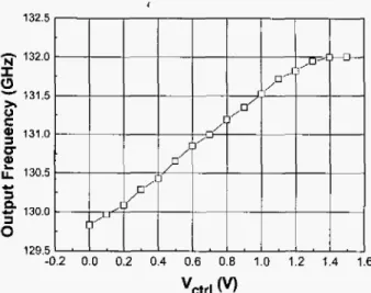
Figure 4 shows the output frequency versus the control voltage (Yctrl), where Vdd fixed at 1 V. The output frequency covers from 129.8 to 132 GHz, with tuning range of 1.7%. Figure 5 shows that the measured phase noise at the fundamental port is -1 14.4dBc/Hz at 10 MHZ offset, and the phase noise at the push-push port is expected to be 6 dB higher.
Hkrl 129.883 GHz
Ref -1s dBm Err M& -41.02 dBn No“ I t I 1 1 I I i r l Lo9 18 dB/ s1u Canto
Rea BCI 3 HHZ w n 3 HHZ S m e u 5 m3 (601 PIS)
Fig. 3.
the W-band spectrum analyzer.
The output spectrum at the push-push port shown on
IV. CONCLUSION
A 131 GHz cross-coupled push-push VCO is designed, fabricated, and tested. It can be tuned from 129.8 to 132 GHz with an estimated phase noise o f -108.4 dBc/Hz at lOMHz offset.
To
the authors’ knowledge, the oscillation frequency is the highest among CMOS VCOs. It also provides up to +2.1dBm
output power at the V-band fundamental differential ports. IACKNOWLEDGEMENTS
This work is supported by NTU-TSMC Joint- Development Project and National Science Council of Taiwan, R. 0. C. (NSC 93-2752-E-002-002-PAE, NSC 93-22 19-E-002-016, NSC 93-22 13-E-002-033, and NSC 93-22 19-E-002-024).
1 1.2 1.4 1.6
V c t r l O Fig. 4.
voltage ( V 3 .
Output frequency at push-push port versus the control
Fig. 5 . Output spectrum at the fundamental port.
REFERENCES
[ I ] K. W. Kobayashi, A. K. Oki, L. T. Tran, J. C. Cowles, A.
Gutierrez-Aitken, F. Yamada, T. R. Block, and D. C. Streit, “A 108-GHz InP-HBT monolithic push-push VCO with low phase noise and wide tuning bandwidth,” IEEE Joumul
of Solid-Sfate Circuits, vol. 34, no, 9, pp, 1225 - 1232, Sep.
1999.
[2] Y . Baeyens, C. Dorschky, N. Weimann, Q, Lee, R. Kopf, G. Georgiou, J.-P. Mattia, R. Ha”, and Y.-K. Chen, “Compact InP-Based HBT VCOs with a Wide Tuning Range at W- and D-Band,” IEEE Trans. on Microwave Theory and Techniques, vol. 48, no. 12, pp. 2403-2408,
Dec. 2000.
[3] S. Kudszus, W. H. Haydl, A. Tessmann, W. Bronner, and M. Schlechtweg, “Push-push oscillators for 94GHz and
I4OGHz applications using standard pseudomorphic GaAs PHEMT,” IEEE MTT-S Int. Microwave Symp. Dig., vol. 3, pp.1571-1574, May. 2001.
[4] Y . Baeyens and Y. K. Chen, “A monolithic integrated
15OGHz SiGe HBT push-push VCO with simultaneous V-
band outputs,” lEEE MTT-S Int. Microwave Symp. Dig.,
vol. 2 , pp. 877-880, Jun. 2003.
[ 5 ] M. Steinhauer, H. Irion, M. Schott, M. Thiel, H.-0. Ruoso, and W. Heinrich, “SiGe-based circuits for sensor applications beyond IOOGHz,” IEEE MTT-S Int. Microwave
Symp. Dig., vol. 1, pp. 223-226, Jun. 2004.
[6] C.-M. Huang, L. Shi, I. Laguado, and
K.
K. 0, “A 25.9GHz voltage-controlled oscillator fabricated in a CMOS process,” Symp. VLSI Circuits Dig. Tech. Papers, pp. 100- 101, Jun. 2000.[7] J.-0. Plouchart, J. Kim, N. Zamdmer, M. Sherony, Y. Tan, M. Yoon, M. Talbi, A. Ray, and L. Wagner, “A 31GHZ
CML ring VCO with 5.4 ps delay in 0. 12-pm SO1 CMOS
technology,” IEEE European Solid-Stufe Conj, p p . 357-
360, Sep. 2003.
[SI C.-C. Chang, R.-C. Liu, and H. Wang, “A 40-GHz push-
push VCO using 0.25-mm CMOS technology,” in 2003
Asia-Pacific Microwave Conference Proceedings, vol. 1 , pp. 73-76,2003.
e
N. Fong, J. Kim, J . - 0 . Plouchart, N. Zamdmer, D. Liu,
JEEE, L. Wagner, C . Plett, and G. Tarr, “A low-voltage
40-GHz complementary VCO with 15% frequency tuning range in SO1 CMOS technology,” IEEE Journal ofSolid-
Stute Circuits, vol. 39, no. 5 , pp. 841-846, May 2004.
A. P. van der Wel, S. L. J. Gierkink, R. C , Frye, V.
Boccuzzi. and B. Nauta, “A robust 43-GHz VCO in CMOS for OC-768 SONET applications,” IEEE Journal ofSaEid-Sfate Circuits, vol. 39, no. 7, pp. 1159-1 163, Jul.
2004.
H . M. Wang, “A 50 GHz VCO in 0.25 pm’CMOS,” ZEEE
ISSCC Dig. Tech. Papers, pp.372-373, Feb. 2001.
M. Tiebout, H.
D.
Wohlmuth, and W. Simburger, “A IV51GHz fully-integrated VCO in O.12pm CMOS,” IEEE
ISSCC Dig, Tech. Papers, pp.238-239, Feb. 2002. H. Shigematsu,
T.
Hirose, F. Brewer, and M. Rodwell, “CMOS circuit design for millimeter-wave applications,”IEEE RFIC Symp. Dig. Tech. Papers, pp. L23-126, Jun. 2004.
F. Ellinger, T. Morf, G. Buren, C. Kromer, G. Sialm, L.
Rodoni, M. Schmatz, and H. Jackel, “60GHz VCO with
wideband tuning range fabricated on VLSI SO1 CMOS
TABLE 1
technology,” IEEE MTT-S Inf. Microwave Symp. Dig.,
vol. 3, pp. 1329-1332, Jun. 2004.
R.-C. Liu, H.-Y. Chang, C.-S. Wang, and H. Wang, “A 63GHz VCO using 0.25pm CMOS,” IEEE ISSCC Dig.
Tech. Papers, vol. 1 , pp.446-447, Feb. 2004.
L.
M.
Franca-Neto, R. E. Bishop, and B. A. Bloechel.,“64GHz and l0OGHz VCOs in 90nm CMOS using optimum pumping method,” IEEE ISSCC Dig. Tech.
Papers, vol.1, pp. 444-538, Feb. 2004.
P.-C. Huang, M.-D. Tsai, and H. Wang, “A 114 GHz VCO in 0. I3pm CMOS,” IEEE ISSCC Dig. Tech. Pupem,
vol. 1, pp. 404-405, Feb. 2005.
H, Veenstra, E. van der Heijden, “A 35.2-37.6GHz LC
VCO in a 701100GHz fT/f,,,,, SiGe technology,” IEEE ISSCC Dig. Tech. Papers, vol+ I , pp. 394-534, Feb. 2004.
J. Jeong and Y. Kwon, “lnjection-Locked push-push
oscillator at 72GHz band using cross-coupled HEMTs,” 2003 European Microwave Conference, vol. 2, pp. 587- 590, Oct. 2003.
PERFORMANCE OF RECENTLY REPORTED CMOS VCOS
*