Metal organic chemical vapor deposition and investigation of ZnO thin films
grown on sapphire
S. Sun
a, G.S. Tompa
a, C. Rice
a, X.W. Sun
b, Z.S. Lee
c, S.C. Lien
c,
C.W. Huang
c, L.C. Cheng
c, Z.C. Feng
c,⁎
aStructured Materials Industries, Inc. 201 Circle Drive N., Unit 102 and 103, Piscataway, NJ 08854, USA bSchool of Electrical and Electronic Engineering, Nanyang Technological University, Singapore 639798, Singapore
cGraduate Institute of Electro-Optical Engineering and Department of Electrical Engineering, National Taiwan University, Taipei, 106-17 Taiwan, ROC
Available online 13 July 2007
Abstract
A new type of large area metal organic chemical vapor deposition (MOCVD) system for the growth of high quality and large size ZnO materials is introduced. Materials properties of the un-doped, n- and p-doped ZnO epi-films grown on sapphire substrates by this MOCVD system are studied by various techniques, including high resolution X-ray diffraction (XRD), UV–Visible optical transmission (OT), photoluminescence (PL) and photoluminescence excitation (PLE), synchrotron radiation X-ray photoelectron spectroscopy (SR-XPS). The wurtzite (w) ZnO crystal structures grown with primary (0002) orientation were identified. Results have shown the high crystalline quality of MOCVD-grown ZnO films, indicated by the narrow XRD, PL and Raman line widths, strong PL signals, sharp OT edge and smooth surface. In particular, high p-type carrier concentration ofN1017cm− 3have been achieved besides the good n-type doping in ZnO.
© 2007 Elsevier B.V. All rights reserved.
Keywords: ZnO; MOCVD; X-ray diffraction; Raman scattering; Photoluminescence; Synchrotron radiation
1. Introduction
Recently, there arises much interest in the research and development on ZnO and related materials. ZnO possesses a room temperature (RT) wide directly band gap of about 3.37 eV
[1]and a large exciton binding energy of 59 meV (NGaN of
28 meV) that make it suitable to applications in light emitting diodes (LEDs), lasers, solar cell, and transparent transistors[1–
15]. These applications require high quality ZnO materials with good uniformity and controllable for thickness and doping level (in both n and p-type). Metal organic chemical vapor deposition (MOCVD) is an excellent technology to achieve above applications and requirements.
The advantage should translate to an even brighter light emission than that obtained with GaN photonics. Un-doped ZnO typically exhibits n-type conductivity, and can be made strongly n-type by growth in zinc-rich conditions or by extrinsic doping
with group-III elements such as Al, Ga or In[16]. For ZnO thin films, n-type conductivity is relatively easy to realize. Until recently, ZnO thin films have proven difficult to dope p-type. This is a fairly common occurrence in wide band-gap semiconductors. In ZnO thin films, most candidate p-type dopants introduce deep acceptor levels. For example, Cu introduces an acceptor level with energy 0.17 eV below the conduction band.
New ZnO-MOCVD systems and process technologies for single and multi-component oxides have been developed recently at Structured Materials Industries, Inc. (SMI) [17]. This paper reports on the MOCVD growth and characterization of a series of ZnO epi-films, un-doped, n-type, and p-type, grown on sapphire by using a new 6 by 2 inch wafer ZnO-MOCVD system under different growth conditions. This reactor uses new patent pending multi-zone filament heater technology— including a shaft heater. In parallel work, this reactor design has also been scaled to deposit on 38–2 inch wafers per deposition run. A variety of techniques, including the high resolution X-ray diffraction (XRD), synchrotron radiation X-ray photoelectron spectroscopy (SR-XPS), optical transmission (OT), photoluminescence (PL), and photolumines-cence excitation (PLE) have been employed to investigate their
Available online at www.sciencedirect.com
Thin Solid Films 516 (2008) 5571–5576
www.elsevier.com/locate/tsf
⁎ Corresponding author. Tel.: +886 2 3366 3543; fax: +886 2 2367 7467. E-mail addresses:[email protected](X.W. Sun),
[email protected](Z.C. Feng).
0040-6090/$ - see front matter © 2007 Elsevier B.V. All rights reserved. doi:10.1016/j.tsf.2007.07.030
optical and structural properties. These experiment results provide useful information about fabrication of ZnO thin film materials. 2. Experiment
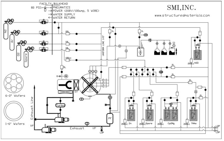
A zinc oxide MOCVD system is designed and built by
Structured Materials Industries (SMI). Fig. 1 shows its
schematic diagram. The reactor uses the vertical growth configuration with a high speed rotation disk. It is of a vertical orientation built to all metal UHV standards. Metalorganics are used for zinc and dopant sources which are to optimize performance at low pressures. The tools can produce amor-phous/poly or epitaxy uniform ZnO with controllable doping and smooth, pinhole-free films, or nanowires, based on process conditions. The precursors used for the MOCVD growth of ZnO and related conditions are offered by SMI as shown inTable 1. General process condition ranges, using such precursors, are as follows: growth pressure from a few Torr to a few tens of Torr, total flows from a few thousand sccm to several thousand sccm, film deposition temperature from 350 °C to 650 °C for general contact work, and precursor rate limiting species pressure (in the reactor) from about 10 mTorr to 50 mTorr.
In order to enhance N incorporation into the depositing film, SMI has used plasma activation. SMI accomplished this using an upstream plasma source, enhancing the availability and reactivity of nitrogen radicals to the depositing film, thus increasing the incorporation/activation rate. This deposition approach is superior
to the prior art because SMI's system is designed to exert independent process control over each of the process parameters, which include physical distribution of the reactants within the reactor, level of activation of the reactants (i.e. degree of nitrogen and/or oxygen plasma activation independent of carrier, other
Fig. 1. Schematics of a ZnO MOCVD system designed by Structured Materials Industries, Inc (SMI).
Table 1
Precursors used for the MOCVD growth of ZnO
Vp/t Comments Precursor Diethyl zinc 15.9 T/25 °C Alloying elements: Mg, Cd, Mn Cp2Mg 0.35 T/50 °C Temp. sensitive Dimethyl cadmium 108.2 T/25 °C
Cp2Mn, Mn (thd)3 Low vp Cp2Mn: toxic; thd, use FE
n–type dopants: Al, Ga, F
Trimethyl aluminum 11.5 T/25 °C Trimethyl gallium 226.5 T/25 °C
Triethyl gallium 6.73 T/25 °C Easier for doping than TMGa
HF Gas Corrosive
p-type dopants: P, As, N, Li
Tert-butyl phosphine 263.98 T/25 °C Tert-butyl arsine 151.09 T/25 °C
Triethyl arsine 8.21 T/25 °C Easier for doping than TBA Li tert-butoxide 0.01 T/110 °C Semi–insulting dopant N2, N2O, NH3, NO Gases Plasma usu. necessary
oxidizer and metalorganics), partial pressures of each process gas, deposition pressure, deposition temperature, and so on. We used the X-ray diffraction (XRD), synchrotron radiation X-ray photoelectron spectroscopy (SR-XPS), optical transmission (OT), photoluminescence (PL), and photoluminescence excita-tion (PLE) to characterize the material properties and compare the difference of the obtained spectra to define the quality of the samples.
3. Results and discussion 3.1. Optical transmission (OT)
Fig. 2shows the UV–visible optical transmission spectra of
ZnO, undoped, p-type and n-type, measured at room temper-ature (RT).Fig. 3shows the determination of the optical gap, Eog, from UV–Visible transmission, for these three ZnO films
grown on sapphire by MOCVD. 3.2. Photoluminescence (PL)
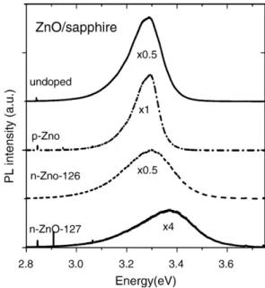
Fig. 4shows the PL spectra, excited under a HeCd 325 nm laser line, for four ZnO films grown on sapphire by MOCVD. Three samples, undoped, p-doped and one n-doped, possess a PL peak at∼3.28 eV, characteristic of the band edge emission from wurtzite ZnO crystal. Another n-type ZnO sample #126, with the spectrum at the bottom curve inFig. 4, shows the PL peak shift from 3.28 eV to 3.38 eV in comparison with the ZnO #127, which indicates a high doping level of this ZnO film. This PL peak shift can be also induced by different amount of strains
within the ZnO film [18,19]. PL spectra show change with
annealing.
3.3. Photoluminescence excitation (PLE)
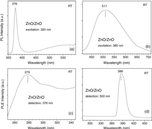
Figs. 5 and 6show the photoluminescence excitation (PLE), plus PL for comparison, spectra from two MOCVD-grown ZnO films grown on bulk ZnO and sapphire, respectively. These PLE and combined PL measurements were performed via a J-Y commercial system using a white light Xe lamp source. Different PL excitation wavelengths and different PLE detection wavelengths were used to exhibit more significant
spectral features for two experimental samples. For the MOCVD-grown ZnO film on ZnO substrate, PL spectrum in
Fig. 5(a) with the excitation of 320 nm, above the band gap of ZnO, exhibits the near band edge emission with the peak at 376 nm and broad features in the green spectral range. As using the excitation of 380 nm, i.e. near the ZnO band gap, the broad green emissions with the peak at∼511 nm are shown. While the PLE spectra for this ZnO/ZnO sample shows the high excited state broad absorption near 279 nm, i.e. 4.4 eV at detection of 376 nm (Fig. 5(c)), i.e. the peak energy of the band edge PL emission, and an absorption band at 386 nm, i.e. slightly below the ZnO band gap, at detection of 500 nm, i.e. on the top of the green emission band (Fig. 6(d)).
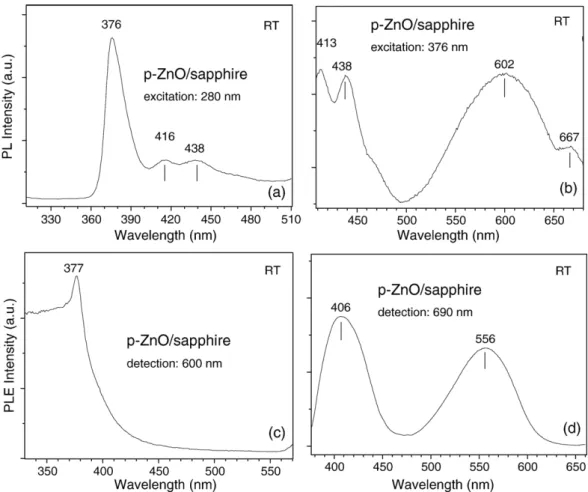
For the MOCVD-grown p-type ZnO film on sapphire substrate, PL spectrum in Fig. 6 (a) under the excitation of 280 nm, above the band gap of ZnO, exhibits the ZnO band edge emission at 376 nm and two features at 416 nm and 438 nm. As using the excitation of 376 nm at the ZnO band gap or the top of band edge emission, these two spectral features are still seen, plus broad emissions covering green-origin-red (Fig. 6 (d)).
Fig. 4. Mirco-PL spectra, excited under 325 nm, of the undoped, p-type and n-type ZnO films grown on sapphire substrates by MOCVD.
Fig. 3. Determination of the optical gap, Eog, from UV–Visible transmission, for
three ZnO films grown on sapphire by MOCVD.
Fig. 2. UV–Visible transmission of three ZnO films grown on sapphire by MOCVD.
5573 S. Sun et al. / Thin Solid Films 516 (2008) 5571–5576
While the PLE spectra for this ZnO/sapphire sample shows the high excited state broad absorption near 279 nm, i.e. 4.4 eV at detection of 376 nm (Fig. 6(c)), i.e. the peak energy of the band edge PL emission, and an absorption band at 386 nm, i.e. slightly below the ZnO band gap, at detection of 500 nm, i.e. on the top of the green emission band (Fig. 6(d)).
3.4. Visible Raman scattering
Fig. 7shows the micro-Raman scattering spectra for three ZnO films, under the excitation of 488 nm from an Ar+laser. A sharp peak at 437 cm− 1is observed for all ZnO samples, which is the wurtzite ZnO characteristic E2mode. The intensity and
full width at half maximum (FWHM) of the E2 mode was
employed to represent the quality of ZnO materials. Higher intensity, narrow and symmetric features indicate the quality of our MOCVD-grown ZnO films on sapphire substrate with high crystalline quality.
3.5. Resonant Raman scattering
Raman scattering measurements on our experimental ZnO samples were also performed using UV excitation of 325 nm from a HeCd laser.Fig. 8shows These Raman spectra for three ZnO films. As seen, a strong A1symmetry longitudinal optical
(LO) phonon mode, 1LO at 556 cm− 1, and its second order 2LO
mode are observed for all samples. The spectral rising in the high frequency side inFig. 8is from the ZnO edge mission PL band. In comparison with the visible Raman spectra ofFig. 7under the
488 nm excitation, where no A1(LO) and 2LO modes could be
detected. Now, under the UV 325 nm excitation beyond the ZnO band gap, the PL band tail has induced and enhanced the A1(LO)
and 2LO modes through the resonant Raman scattering process. 3.6. Synchrotron radiation X-ray photoelectron spectroscopy (SR-XPS)
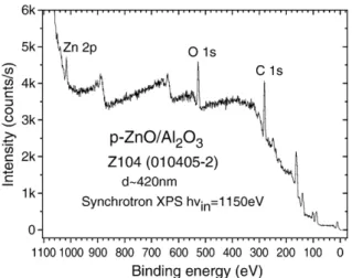
In order to study the surface oxidizations and estimate the degree of pollutions by carbon, we arrange a synchrotron radiation X-ray photoelectron spectroscopy (SR-XPS) experiments on the 24A1 beamline of National Synchrotron Radiation Research Center (NSRRC) in Hsinchu, Taiwan (R.O.C.). SR-XPS experiments were performed using a monochromatic X-rays beam with 1150 eV incident light energy. The constant analyzer energy (CAE) mode was used with analyzer pass energy of 200 eV for preliminary wide scan (Fig. 9). The binding energy of C 1s, O 1s, and Zn 2p were observed at 285.01, 531.01, and 1020 eV, respectively.
4. Conclusion
In this paper, a new type of metalorganic chemical vapor deposition (MOCVD) system for the growth of high quality and
large size ZnO materials is introduced. Materials properties of the un-doped, n- and p-doped ZnO epi-films grown on sapphire substrates by this MOCVD system are reported. Materials were characterized by various techniques. Photoluminescence (PL) indicated the w-ZnO band edge emission band near 3.3 eV and the variation of the PL peak with the doping levels. UV–Visible optical transmission (OT) measurements gave the optical gap values, corresponding to the PL results. Visible Raman
scattering showed the w-ZnO characteristic E2phonon mode
and UV 325 nm excited resonant Raman scattering exhibited
the A1(LO) and 2LO phonon modes which were enhanced due
to the resonance with the fundamental ZnO PL band.
Synchrotron radiation X-ray photoelectron spectroscopy (SR-XPS) showed the surface oxidizations and estimated the degree of pollutions by carbon.
All results have shown the high crystalline quality of MOCVD-grown ZnO films, indicated by the narrow XRD, PL and Raman line widths, strong PL signals, sharp OT edge and smooth surface. In particular, high p-type carrier concentration of up to 1019cm− 3has been achieved besides the good n-type doping in ZnO. New classes of p–n junction devices based on ZnO including blue and UV LEDs, lasers and detectors are
Fig. 8. Resonant Raman spectra of three MOCVD-grown ZnO under the excitation of 325 nm.
Fig. 6. PL and PLE of p-type ZnO film grown on sapphire substrate.
Fig. 7. Raman spectra of three MOCVD-grown ZnO under the excitation of 488 nm.
5575 S. Sun et al. / Thin Solid Films 516 (2008) 5571–5576
expected, based upon our excellent ZnO MOCVD systems and optimization of growth conditions.
Acknowledgment
This work at National Taiwan University was supported by the National Science Council of the Republic of China, NSC 94-2215-E-002-019 and 95-2221-E-002-118.
References
[1] T. Koid, S.F. Chichibu, A. Uedono, T. Sota, A. Tsukazaki, M. Kawasaki, Appl. Phys. Lett. 84 (2004) 1079.
[2] C.X. Xu, X.W. Sun, C. Yuen, B.J. Chen, S.F. Yu, Z.L. Dong, Appl. Phys. Lett. 86 (2005) 011118.
[3] S. Kolesnik, B. Dabrowski, J. Mais, J. Appl. Phys. 95 (2004) 2582. [4] V. Bhosle, A. Tiwari, J. Narayan, Appl. Phys. Lett. 88 (2006) 032106. [5] J.D. Ye, S.L. Gu, S.M. Zhu, S.M. Liu, Y.D. Zheng, R. Zhang, Y. Shi, Q.
Chen, H.Q. Yu, Y.D. Ye, Appl. Phys. Lett. 88 (2006) 101905.
[6] P. Wu, G. Saraf, Y. Lu, D.H. Hill, R. Gateau, L. Wielunski, R.A. Bartynski, D.A. Arena, J. Dvorak, A. Moodenbaugh, T. Siegrist, J.A. Raley, Yung Kee Yeo, Appl. Phys. Lett. 89 (2006) 012508.
[7] Weitao Cao, Weimin Du, Fuhai Su, Guohua Li, Appl. Phys. Lett. 89 (2006) 031902.
[8] D.C. Agarwal, R.S. Chauhan, Amit Kumar, D. Kabriraj, F. Singh, S.A. Khan, D.K. Avasthi, J.C. Pivin, M. Kumar, J. Ghatak, P.V. Satyam, J. Appl. Phys. 99 (2006) 123105.
[9] C.L. Du, Z.B. Gu, M.H. Lu, J. Wang, S.T. Zhang, J. Zhao, G.X. Cheng, H. Heng, Y.F. Chen, J. Appl. Phys. 99 (2006) 123515.
[10] Sang-Moo Park, Tomoaki Ikegami, Kenji Ebihara, Thin Solid Films 513 (2006) 90.
[11] Huichao Zhu, Guotong Du, Xiangping Li, Yuantao Zhang, Yongguo Cui, Keke Huang, Xiaochuan Xia, Tianpeng Yang, Baolin Zhang, Yuchun Chang, Semicond. Sci. Technol. 21 (2006) 1090.
[12] Yang Zhang, Bixia Lin, Xiankai Sun, Zhuxi Fu, Appl. Phys. Lett. 86 (2005) 131910.
[13] G.W. Cong, H.Y. Wei, P.F. Zhang, W.Q. Peng, J.J. Wu, X.L. Liu, C.M. Jiao, W.G. Hu, Q.S. Zhu, Z.G. Wang, Appl. Phys. Lett. 87 (2005) 231903. [14] Masahiro Kunisu, Fumiyasu Oba, Hidekazu Ikeno, Isao Tanaka, Tomoyuki
Yamamoto, Appl. Phys. Lett. 86 (2005) 121902.
[15] Tae-Bong Hur, Yoon-Hwae Hwang, Hyung-Kook Kim, J. Appl. Phys. 96 (2004) 1507.
[16] Y. Ma, G.T. Du, S.R. Yang, Z.T. Li, B.J. Zhao, X.T. Yang, T.P. Yang, Y.T. Zhang, D.L. Liu, J. Appl. Phys. 95 (2004) S55.
[17] Web of Structured Materials Industries, Incorporated: http://www.struc-turedmaterials.com/.
[18] R. Ghosh, D. Basak, S. Fujihara, J. Appl. Phys. 96 (2004) 2689. [19] O. Kappertza, R. Drese, M. Wuttig, J. Vac. Sci. Technol., A, Vac. Surf.
Films 20 (2002) 2084. Fig. 9. Synchrotron radiation XPS of the p-type ZnO film grown on sapphire