Study of thermal stability of nickel monogermanide on single- and polycrystalline
germanium substrates
Shih-Lu Hsu, Chao-Hsin Chien, Ming-Jui Yang, Rui-Hao Huang, Ching-Chich Leu, Shih-Wen Shen, and Tsung-Hsi Yang
Citation: Applied Physics Letters 86, 251906 (2005); doi: 10.1063/1.1953880 View online: http://dx.doi.org/10.1063/1.1953880
View Table of Contents: http://scitation.aip.org/content/aip/journal/apl/86/25?ver=pdfcov
Published by the AIP Publishing
Articles you may be interested in
Effect of pinning by an orientation gradient on the thermal stability of ultrafine grained Ni produced by equal channel angular pressing
J. Appl. Phys. 115, 113503 (2014); 10.1063/1.4867416
Effect of Mo interlayer on thermal stability of polycrystalline NiSi thin films
J. Appl. Phys. 101, 063544 (2007); 10.1063/1.2714490
Formation of nickel silicide and germanosilicide layers on Si(001), relaxed Si Ge Si ( 001 ) , and strained Si/relaxed Si Ge Si ( 001 ) and effect of postthermal annealing
J. Vac. Sci. Technol. A 24, 1468 (2006); 10.1116/1.2210942
F-enhanced morphological and thermal stability of NiSi films on BF 2 + -implanted Si(001)
Appl. Phys. Lett. 81, 5138 (2002); 10.1063/1.1533856
Comparison of the thermal stability of NiSi films in Ni/Pt/(111)Si and Ni/Pt/(100)Si systems
J. Appl. Phys. 90, 745 (2001); 10.1063/1.1379053
This article is copyrighted as indicated in the article. Reuse of AIP content is subject to the terms at: http://scitation.aip.org/termsconditions. Downloaded to IP: 140.113.38.11 On: Thu, 01 May 2014 02:58:52
Study of thermal stability of nickel monogermanide on single- and
polycrystalline germanium substrates
Shih-Lu Hsu, Chao-Hsin Chien,a兲Ming-Jui Yang, Rui-Hao Huang, Ching-Chich Leu, and Shih-Wen Shen
National Nano Device Laboratories, 1001-1 Ta-Hsueh Rd., Hsin-Chu 300, Taiwan
Tsung-Hsi Yang
Department of Materials Science and Engineering, National Chiao Tung University, 1001 Ta-Hsueh Rd., Hsin-Chu 300, Taiwan
共Received 20 October 2004; accepted 24 May 2005; published online 14 June 2005兲
We have investigated the thermal stability of nickel monogermanide共NiGe兲 films formed by rapid thermal annealing on both single- and polycrystalline Ge substrates. We found that the NiGe phase is the only one present after nickel germanidation in the temperature range 400– 700 ° C. A fairly uniform NiGe film formed on the single-crystalline Ge; it possessed excellent resistivity
共15.6 ⍀ cm兲 and was thermally stable up to 550 °C, but it degraded rapidly at higher temperatures
as a result of agglomeration. In contrast, the NiGe film formed on the polycrystalline Ge exhibited much poorer thermal stability, possibly because of polycrystalline Ge grain growth, which resulted in columnar NiGe grains interlaced with Ge grains that had a dramatically increased sheet resistance. As a result, we observed that the sheet resistances of NiGe lines subjected to annealing at 500 ° C depended strongly on the linewidth when this width was comparable with the grain size of the polycrystalline Ge. © 2005 American Institute of Physics. 关DOI: 10.1063/1.1953880兴
An extensive amount of renewed interest in Ge sub-strates has occurred recently because of their superior elec-trical properties, especially their higher mobility, when com-pared with their Si counterparts.1,2For instance, the selective deposition of Ge can result in a relatively low contact resis-tance for a self-aligned raised source and drain structure, as well as a suppression of the short channel effect.3 To inte-grate Ge into current device processing, however, requires a thermally stable and uniform low-resistivity metal germanide film. Among the metal silicides, nickel monosilicide共NiSi兲 is the one of the most promising candidates for sub-100-nm technologies because of its low formation temperature, low resistivity 共14–20⍀ cm兲, low consumption of Si, resis-tance to bridging failure, and lack of resistivity degradation on narrow lines or gates.4 These beneficial features of NiSi motivated us to investigate the mechanism of formation and thermal stability of NiGe formed on both single- and poly-crystalline Ge substrates.
In this study, we used Ga-doped p-type single-crystalline 2 in. Ge共100兲 wafers having a resistivity of 0.05 ⍀ cm and undoped 125 nm thick polycrystalline Ge thin films having a sheet resistance larger than 1 k⍀/sq deposited on oxidized 6 in. Si共100兲 wafers through ultrahigh-vacuum chemical va-por deposition.5After dipping them in dilute HF solution, we loaded the wafers immediately into an electron-beam evapo-ration system operating at a base pressure of 1.0
⫻10−6Torr. A 20 nm thick Ni film was then deposited onto
the single- and polycrystalline Ge surfaces at room tempera-ture with a rate of 1 Å / s. Nickel germanidation reactions on the blank and patterned wafers were performed through rapid thermal annealing 共RTA兲 at various temperatures for 30 s under a flowing N2 atmosphere. We measured the sheet
re-sistance of nickel germanide by using a four-point probe
method and used bridge resistor structures to investigate the effect of the linewidth on the sheet resistance of NiGe. Phase identification was performed using x-ray diffraction共XRD兲 measurements in the conventional– 2 geometry. We ana-lyzed the microstructures and compositions of the nickel ger-manide samples using cross-sectional transmission electron microscopy 共XTEM兲 and energy-dispersive spectrometry
共EDS兲.
Figures 1共a兲 and 1共b兲 present the XRD spectra of the nickel germanide formed on single- and polycrystalline Ge substrates, respectively, at different RTA temperatures. For the nickel germanide formed on the single-crystalline Ge, all of the peaks observed in the temperature range of 400– 700 ° C identify the orthorhombic NiGe phase. At lower temperatures, the peak profiles of NiGe remained vir-tually unchanged, but the relative intensity of the NiGe peak in the共111兲 orientation increased and the full width at half maximum narrowed upon increasing the temperature. These tendencies indicate that the共111兲 orientation is preferred for NiGe grains during high-temperature annealing, possibly be-cause of the fact that the surface energy of NiGe in the共111兲 orientation is the smallest among all of the possible orienta-tions. We found, however, that the intensities of the peaks decreased significantly after annealing at 700 ° C; this phe-nomenon may arise from a structural change of the NiGe grains, but the mechanism needs further investigation. For the nickel germanide formed on the polycrystalline Ge, we observed that NiGe was also the only phase after annealing. None of the peaks underwent any observable change upon increasing the annealing temperature, except for that of the polycrystalline Ge共111兲 orientation. This result suggests that the共111兲-oriented polycrystalline Ge grains can undergo fur-ther growth during nickel germanidation. Using Scherrer’s formula, we estimated the average grain sizes of polycrystal-line Ge for the 共111兲 orientation to be 26, 28, 32, 38, and 52 nm after annealing at 400, 500, 550, 600, and 700 ° C,
a兲
Electronic mail: [email protected]
APPLIED PHYSICS LETTERS 86, 251906共2005兲
0003-6951/2005/86共25兲/251906/3/$22.50 86, 251906-1 © 2005 American Institute of Physics
This article is copyrighted as indicated in the article. Reuse of AIP content is subject to the terms at: http://scitation.aip.org/termsconditions. Downloaded to IP: 140.113.38.11 On: Thu, 01 May 2014 02:58:52
respectively. Clearly, steep increases in the polycrystalline Ge grain size occur at temperatures above 500 ° C.
Figure 2 displays the sheet resistance of the NiGe film as a function of the RTA temperature. For comparison, the sheet resistance of the NiSi film formed on the single-crystalline Si is also presented. It is clear that the sheet resistance of the NiSi film, which is well known to be the stable phase at temperatures above 450 ° C, remains in a low-resistivity state at temperatures up to 700 ° C. NiGe exhibits poorer thermal stability than NiSi, however, and its sheet resistance in-creased drastically at relatively low temperatures. In the case of the single-crystalline Ge, we attribute the cause of the dramatic increase in the resistance observed at temperatures above 550 ° C to the agglomeration of the NiGe film,
be-cause the formation of a high-resistivity phase is ruled out by the XRD results. On the other hand, in the case of the poly-crystalline Ge, the rapid degradation in sheet resistance that occurred at temperatures above 500 ° C can be associated with the grain growth, which is supported by the previous results. Indeed, similar behavior has been observed in studies of silicides formed on polycrystalline Si,6–8and it has been ascribed to the formation of discontinuous silicide films in-duced by polycrystalline Si grain growth beneath the surface. The driving force for this grain growth is believed to be the reduction of the grain boundary and interface energies.6–8It is also noteworthy that the lowest value of sheet resistance of the NiGe film formed on the polycrystalline Ge is slightly higher than that of the others共see the discussion below兲.
Figures 3共a兲 and 3共b兲 present XTEM micrographs of NiGe formed on the single-crystalline Ge at 450 and 600 ° C, respectively. We observed clearly that the NiGe annealed at 450 ° C, which is the sample having the lowest resistance, exhibits a fairly uniform film having a thickness of 48 nm and resistivity of 15.6⍀ cm, which is comparable with that of NiSi 共14–20⍀ cm兲. After annealing at 600 °C, how-ever, severe agglomeration and separation of NiGe occurred, which is consistent with our observed sheet resistance behav-ior. It is apparent, therefore, that the NiGe film is less ther-mally stable morphologically than is the NiSi film. We at-tribute this result to the lower surface energy of Ge and the lower melting point of NiGe, with respect to its counterpart, because both the lower surface energy of Ge and the higher migration of NiGe can accelerate the rate of agglomeration.9–11Figures 3共c兲 and 3共d兲 display XTEM mi-crographs of NiGe formed on the polycrystalline Ge at 450 and 550 ° C, respectively. After annealing at 450 ° C, the NiGe film共thickness: ⬃48 nm兲 is also uniform, but it has a relatively rough surface and interface between the NiGe film and the polycrystalline Ge; this situation may arise from the initial roughness of the polycrystalline Ge film, which, there-fore, results in the slightly higher resistivity 共18.4⍀ cm兲.
FIG. 1. XRD spectra of nickel germanide formed on共a兲 single- and 共b兲 polycrystalline Ge substrates at different RTA temperatures.
FIG. 2. The sheet resistances of the NiGe film plotted as a function of the RTA temperature. For comparison, the sheet resistances of the NiSi film formed on single-crystalline Si are also included.
FIG. 3. XTEM micrographs of NiGe formed on the single-crystalline Ge annealed at共a兲 450 and 共b兲 600 °C, and on the polycrystalline Ge annealed
at共c兲 450 and 共d兲 550 °C.
251906-2 Hsuet al. Appl. Phys. Lett. 86, 251906共2005兲
This article is copyrighted as indicated in the article. Reuse of AIP content is subject to the terms at: http://scitation.aip.org/termsconditions. Downloaded to IP: 140.113.38.11 On: Thu, 01 May 2014 02:58:52
After annealing at 550 ° C, however, the uniform NiGe film disappeared and we observed only columnar NiGe and Ge grains, which we identified through EDS analysis. We be-lieve that this phenomenon arose from polycrystalline Ge grain growth induced by the NiGe during annealing. These gradually enlarged polycrystalline Ge grains penetrated into the upper NiGe film and then triggered the downward diffu-sion of Ni to form the columnar NiGe grains. Eventually, the columnar NiGe and Ge grains interlaced. Obviously, this broken NiGe film accounts for the drastic increase in the resistance that we observe in Fig. 2. The XRD results also provide evidence for grain growth and suggest that the Ge grains grew at temperatures above 500 ° C.
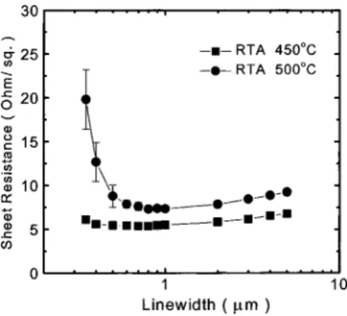
Figure 4 presents the sheet resistances, as a function of the annealing temperature, of the NiGe films of different linewidths that were formed on the polycrystalline Ge. After annealing at 450 ° C, the sheet resistance remained nearly constant as the linewidth decreased, suggesting that the for-mation of NiGe is independent of the linewidth. After an-nealing at 500 ° C, however, the sheet resistance increased, especially when the linewidth shrank to below 0.5m. The higher resistance is due to the rougher interface between the NiGe film and the polycrystalline Ge that is caused by grain
growth; as the linewidth is scaled down to a level compa-rable with the grain size, the upwardly growing polycrystal-line Ge grains may break the continuity of the NiGe polycrystal-lines and result in the rapid increase observed in the sheet resis-tance.
We have investigated the thermal stability of NiGe formed on both single- and polycrystalline Ge substrates through RTA processing. On single-crystalline Ge, the uni-form NiGe film that uni-formed was thermally stable up to 550 ° C. When the annealing temperature increased, agglom-eration of the NiGe resulted in a dramatic increase in its sheet resistance. For the NiGe formed on the polycrystalline Ge, the rougher surface and interface led to a slight increase in the sheet resistance of the NiGe film and the thermal sta-bility was severely degraded by NiGe-induced line Ge grain growth. When the linewidth of the polycrystal-line Ge was comparable with the grain size, we observed a tremendous increase in the degradation in the sheet resis-tance of the NiGe lines after annealing at 500 ° C.
This project was sponsored by the National Science Council, the Republic of China共Contract No. 93A0501兲.
1
A. Ritenour, S. Yu, M. L. Lee, N. Lu, W. Bai, A. Pitera, E. A. Fitzgerald, D. L. Kwong, and D. A. Antoniadis, Tech. Dig. - Int. Electron Devices Meet. 2003, 18.2.1.
2
C. O. Chui, H. Kim, D. Chi, B. B. Triplett, P. C. McIntyre, and K. C. Saraswat, Tech. Dig. - Int. Electron Devices Meet. 2002, 437.
3
Y.-K. Choi, D. Ha, T.-J. King, and C. Hu, IEEE Electron Device Lett. 22,
447共2001兲.
4
T. Morimoto, T. Ohguro, H. S. Momose, T. Iinuma, I. Kunishima, K. Suguro, I. Katakabe, H. Nakajima, M. Tsuchiaki, M. Ono, Y. Katsumata, and H. Iwai, IEEE Trans. Electron Devices 42, 915共1995兲.
5
G. Luo, T.-H. Yang, E. Y. Chang, C.-Y. Chang, and K.-A. Chao, Jpn. J. Appl. Phys., Part 2 42, L517共2003兲.
6
S. Nygren and S. Johansson, J. Appl. Phys. 68, 1050共1990兲.
7
S. Nygren, D. Caffin, M. Östling, and F. M. d’Heurle, Appl. Surf. Sci. 53,
87共1991兲.
8
E. G. Colgan, J. P. Gambino, and B. Cunningham, Mater. Chem. Phys. 46,
209共1996兲.
9
T. P. Nolan, R. Sinclar, and R. Beyer, J. Appl. Phys. 71, 720共1992兲.
10
P. C. Kelires and J. Tersoff, Phys. Rev. Lett. 63, 1164共1989兲.
11
T. B. Massalski, Binary Alloy Phase Diagrams共American Society for Metals, Metal Park, OH, 1986兲.
FIG. 4. The sheet resistances, plotted as a function of the annealing tem-perature, of NiGe films of different linewidths formed on the polycrystalline Ge.
251906-3 Hsuet al. Appl. Phys. Lett. 86, 251906共2005兲
This article is copyrighted as indicated in the article. Reuse of AIP content is subject to the terms at: http://scitation.aip.org/termsconditions. Downloaded to IP: 140.113.38.11 On: Thu, 01 May 2014 02:58:52