國立交通大學
顯示科技研究所
碩士論文
交流型電漿顯示器之
氧化鎂保護層與面板特性之關係與研究
Relationship between MgO Thin Film
Properties and Panel Performance in AC-PDP
研 究 生:李偉誠
指導教授:金星吾 教授
交流型電漿顯示器之
氧化鎂保護層與面板特性之關係與研究
Relationship between MgO Thin Film
Properties and Panel Performance in AC-PDP
研 究 生: 李偉誠
Student: Wei-Cheng Lee
指導教授: 金星吾 Advisor: Dr. Sung-O Kim
國立交通大學
顯示科技研究所
碩士論文
A Thesis
Submitted to Department of Photonics and Display Institute
College of Electrical Engineering and Computer Science
National Chiao-Tung University
in Partial Fulfillment of the Requirements
for the Degree of Master
in
Display
June 2006
Hsinchu, Taiwan, Republic of China.
交流型電漿顯示器之
氧化鎂保護層與面板特性之關係與研究
研究生:李偉誠 指導教授:金星吾 博士
國立交通大學顯示科技研究所
摘要
隨著電腦科技與網路普及所帶來對人類生活品質的衝擊,各樣具有輕薄短 小、低耗功率等顯示器的需求越來越高,近年來更邁入大尺寸家用型電視市場。 交流型電漿顯示器更成為家用型大型電視的最佳候選人。不需要背光模組的自發 光特性、三十二至一百吋的大尺寸顯示畫面、輕薄懸掛式,以及高畫質電視等特 性,都使得交流型電漿顯示器在這場家用大型電視的大戰中顯得格外的引人注 目。然而,交流型電漿顯示器仍然有關鍵性的問題有待解決。烙痕現象以及顯示 壽命以及消耗功率是現階段即待改善的關鍵議題。有鑒於傳統的交流型電漿顯示 器對於氧化鎂保護層的特性以及面板特性之關係並無專門研究,在此我們將針對 氧化鎂保護層對於烙痕現象以及面板表現的關係提出討論。 此研究的重點在於針對調整改氧化鎂在蒸鍍時的條件,並加以修正已達到產 生出最佳化地保護層膜。以此提高其保護藉電層的功能與時效,以及進一步藉由 其良好的特性提升電漿放電的效率,以達到改善交流型電漿顯示器在亮度、反應 時間、消耗功率以及烙痕方面的缺點。Relationship between MgO Thin Film
Properties and Panel Performance in AC-PDP
Student: Wei-Cheng Lee Advisor: Dr. Sung-O Kim
Department of Photonics and Display Institute, National Chiao Tung University
Abstract
The impact of MgO thin film properties on the performance of AC-Plasma
Display Panels (AC-PDPs) is described. In this study, MgO thin films in AC-PDPs are deposited by e-beam evaporation in which the oxygen flow rate and electron beam
current are varied. Properties of PDP, including luminance, response time, dynamic margin, and color temperature, image sticking are characterized as a function of time
in accelerated aging tests. Besides, both surface analysis and theory demonstrate that a PDP incorporating MgO films grown at reduced O2 flow rates provide improved
panel properties due to a higher density of the MgO film, higher crystallinity and a uniform but relatively surface roughness. In this study, it reveals that MgO deposited
with 10 sccm oxygen flow rate exhibits the highest thin film density compared to others. This high density MgO thin film with a uniform but relatively rough surface
致謝
首先,我要感謝上帝賜給我這個機會能在交通大學的研究所當中學習,除了 知識上的長進,更在人生歷練中往前一大步,感謝神的恩典與帶領。我還要感謝 金星吾指導教授在學業、研究以及英文方面的指導,並且讓我在研究生活當中有 更深的國際觀也在團隊當中學習到團隊精神與合作的重要。 除此之外,我要感謝四位與我一起打拼奮鬥的好伙伴們-吳正宇、周鴻杰、 卓龍材以及任珂銳。第一屆的同袍情誼,讓我深深體會到知心好友的重要。謝謝 你們在日常生活中的照顧與包容,更感謝你們在實驗上的幫助與鼓勵,兩年的共 同生活讓我從你們身上有許多深刻的學習;我還要感謝實驗室助理張雅惠小姐的 細心幫忙與協助;中華映管的陳孝生處長、李建邦經理、黃志明以及許建興工程 師等在專業上面的協助。 最後但也是最重要的,我要感謝我親愛的父母以及弟弟,謝謝你們愛的包 容與無私心的支持;我更要感謝我的女朋友王俐文,謝謝你陪我走過這段時光, 感謝妳在低潮時的陪伴與鼓勵,感謝妳百分百的支持與愛,讓我能咬緊牙關完成 研究所的課程與實驗;我要再一次感謝神賜給我這一切,讓這份喜悅與每位關心 我的人分享。Table of Contents
Abstract (Chinese)………...…….i
Abstract (English) ………...ii
Acknowledgements………..iii
Table of Contents……….iv
Figure Caption………..v
List of Tables………....vi
Chapter 1 Introduction………...1
1.1 Flat Panel Display………...1
1.2 Plasma Display Panel....………...2
1.2.1 Fundamental Structure………4
1.3 Motivation and Objective..………. 7
1.4 Organization………..8
Chapter 2 Principle of Plasma Display Panel………..……….9
2.1 PDP History………..9
2.1.1 Invention of Plasma Display Panel………11
2.1.2 Practical Commercial Structure………...14
2.1.3 Key Features for TV Developments……….17
2.2 Plasma and VUV Generation………19
2.2.1 Principle of Plasma Physics………19
2.2.2 Ionization and Gas Discharge………21
2.2.3 Vacuum Ultraviolet (VUV)…...……...………23
2.3 Driving……….………25
2.4 Protective Layer-MgO………...26
2.4.1 MgO Development in PDP History………27
2.4.2 Chemical and Physical Profile……….………...28
2.5 Summary……….30
Chapter 3 Fabrication and Measurement Instrument……….31
3.1 Introduction………31
3.2 Fabrication Process………33
3.2.1 Front Panel Fabrication ………34
3.2.2 Rear Panel Fabrication ………39
3.2.3 Panel Assembling ………42
3.3 Experimental Setup……….44
3.3 Measurement System……….46
Chapter 4 Experimental Results and Discussion………50
4.1 Introduction………50
4.2 MgO Thin Film Density……….………51
4.3 Dynamic Margin and Response Time………...54
4.4 Luminance Degradation……….………...59
4.4.1 White Color Luminance Degradation………...60
4.4.2 Red Color Luminance Degradation………...61
4.4.3 Green Color Luminance Degradation………...62
4.4.4 Blue Color Luminance Degradation………...63
4.6 Image Sticking Phenomenon……….65
4.6.1 Pre-Work……….………...68
4.6.2 White Image Sticking……….………...69
4.6.3 Dark Image Sticking……….………...72
4.6.4 Color Temperature…….……….………...74
4.6.4 Recovery Ability…….……….………...75
4.7 Analysis of Surface Morphology-AFM……….78
4.8 Investigation of Crystal Structure-XRD……….80
4.9 Summary………..……….81
Chapter 5 Conclusions………..83
5.1 Conclusions……….83
5.2 Future Works……….85
Figure Caption
Fig. 1.1 Plasma display panel………...…….3
Fig. 1.2 Fundamental PDP structure………...………4
Fig. 1.3 Conventional PDP Cell Structure……….…5
Fig. 1.4 Plasma and VUV generation……….…7
Fig. 2.1 Inventor of plasma display panel………..9
Fig. 2.2 Early plasma panel with vacuum system………10
Fig. 2.3 Original drawing of plasma display panel……….………...…12
Fig. 2.4 Early 4x4 pixels presented by UIUC….………...………13
Fig. 2.5 First color plasma panel………14
Fig. 2.6 16x16 pixels presented by UIUC………15
Fig. 2.7 Early open cell structure……….………...…15
Fig. 2.8 128x128 pixels plasma panel with open cell structure………16
Fig. 2.9 A 16x16 pixels plasma panel with 100 Award………17
Fig. 2.10 The visible light emission process………19
Fig. 2.11 What is plasma………20
Fig. 2.12 UV formation……….……...21
Fig. 2.13 Energy level and state of xenon gas………23
Fig. 2.14 ADS driving method………26
Fig. 3.1 Typical T-Shape cell structure………....32
Fig. 3.2 PDP fabrication process………....33
Fig. 3.3 Process for ITO and SnO2………....35
Fig. 3.4 Process for Ag electrode with photolithography………....37
Fig. 3.5 Screen printing method………....38
Fig. 3.7 Phosphor layer deposited by screen printing………....41
Fig. 3.8 Phosphor layer with barrier rib………....42
Fig. 3.9 Assembling process………....43
Fig. 3.10 Experimental PDP module………....46
Fig. 3.11 Optical measurement system………....47
Fig. 3.12 Image pattern generated by axtro 828………....47
Fig. 3.13 Color analyzer CA-100………....48
Fig. 4.1 Trend of MgO thin film density and refractive index………53
Fig. 4.2 Dynamic margin with 100 hours aging (a) No.6, (b) No.2………….…….54
Fig. 4.3 Discharge Lag (a) No.6 (b) No.2 and No.3 (c) No. 1 (d) No.4 and No.5 ...57
Fig. 4.4 Luminance degradation(a)white, (b)red, (c)green, (d)blue………59
Fig. 4.5 Color temperature variation………...……….64
Fig. 4.6 Image sticking phenomenon (a) 4% pattern, (b) measurement system...…65
Fig. 4.7 Image sticking (a) white, (b) dark……….……….64
Fig. 4.8 Luminance of image sticking cells and normal operated ones (a) No.6, (b) No.2 ………... 68
Fig. 4.9 White image sticking (a) No.6, (b) No.2……….……71
Fig. 4.10 Dark image sticking (a) No.6, (b) No.2……….………….……73
Fig. 4.11 Color temperature (a) No.6, (b) No.2……….………….……74
Fig. 4.12 Recovery Ability (a) No.6, (b) No.2……….………….……75
Fig. 4.13 AFM images (a) No.6, (b) No.2………...………….……78
List of Tables
Tab. 2.1 Chemical and physical profile of MgO………...29
Tab. 3.1 Specification of experimental PDP modules……….………...44 Tab. 4.1 MgO thin film density………..………...…..….51
Chapter 1
Introduction
As quality of life of human beings has been greatly valued in recent days,
electronic products capable of light weight, thin volume and low power consumption are then spring up and highly demanded. Among those designs, Flat Panel Display
(FPD) is unquestionably one of the most attractive products. In this chapter, the trend of development of FPDs and characteristics of Plasma Display Panel (PDPs) are
briefly introduced and the objectives of the thesis will be resolved.
1.1 Flat Panel Display
Industry of FPD is now growing up rapidly due to the demand of consumer
electronic product market. For different applications, such as TV, monitor, laptop computer, cell-phone, PDA, and digital camera, varied approaches have been adopted
to achieve these goals. Generally, several well known technologies including Plasma Display Panel (PDP), Liquid Crystal Display (LCD), CRT (Cathode Ray Tube),
Organic Light Emissive Device (OLED) are now the main stream among those approaches in the markets. Until recently, the market for direct-view, flat panel
televisions was segmented fairly clearly, with LCD sets available only in screen sizes smaller than 50 inches, and PDP products available in larger screen sizes ranging from
37 to 103 inches. In the past decade, LCD has become the dominant answer for desktop and laptop computer monitors. The consumer market for these two flat panel
technologies is beginning to converge, due to mass production of LCDs in larger screen sizes.
Nevertheless, it is believed that PDP is the promising candidate for the large sized TV and home theatre applications. Excellent image quality and necessary big
size (more than 100 inches) give PDP the ability to fulfill the dream of building up home theatre in each family. Unlike LCD using Cold Cathode Fluorescent Lamp
(CCFL) as a backlight source, PDP is a self-emissive display, which can provide wide viewing angle, makes it have a CRT like high image quality [1]. Without those
complicated fabricating processes which have been used in LCDs, it only requires several simple technologies to fulfill the fabrication of a PDP module. Accordingly,
the fundamental structure and basic working mechanism of PDPs will be introduced in the next paragraph.
1.2 Plasma Display Panel
Plasma displays are enjoying an unprecedented degree of success as large-screen televisions (TVs). World sales of plasma display modules reached $6 billion in 2005.
Sales are projected to be $8.9 billion by 2007. Plasma TV products are now available in a range of screen diagonals from 32-inch to 80-inch. In the start of 2005, there
shows the appearance of a high quality 102-inch diagonal 1920 x 1080 pixel high definition plasma TV prototype. The U.S. based Consumer Electronics Association’s
October 2004 holiday forecast survey found that plasma TV was the most desired gift for the holiday season [2].
While PDP and LCD offer some shared benefits (flat, thin form factor and undistorted, fixed-pixel image rendering), significant quality differences still remain.
Plasma displays continue to best fill the needs of home theatre enthusiasts seeking premium-quality large-screen display devices, due to several inherent benefits of the
The large area FPD is demanded for a HDTV and a digital TV which displays a real and life-size image in addition to the traditional TV image because of the
development of the both computer and network technologies.
Fig. 1.1 "Now it is just starting to blossom," said Larry Weber of the consumer market for plasma display panel. The figure shows a sharp and bright image quality with a colorful flowers picture.
As shown in Fig. 1.1, PDP’s image quality looks sharp and bright from virtually
anywhere in the room. On the other hand, because plasma TV screens use the phosphor coating (like direct-view and projection CRT TVs), the potential for image
burn-in exists, so it's important to follow the manufacturer's recommendations on day-to-day use. It is known that plasma TVs based on innovative AliS technology
(Alternate Lighting of Surfaces) are proving that even a non-progressive picture can look outstanding [3].
1.2.1 Fundamental Structure
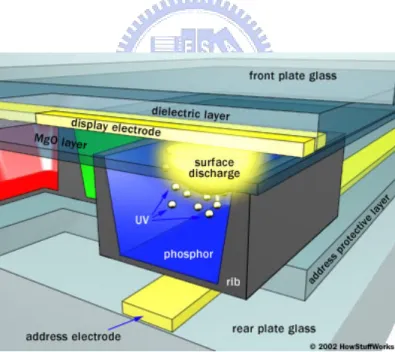
Fig. 1.2 shows the fundamental PDP structure which has been widely used for the TV markets in nowadays. As shown in the figure, a plasma display panel consists of two transparent glass panels (front and rear panel) with a thin layer of pixels
sandwiched in between.
Since a plasma display panel is illuminated at the sub-pixel level, images are
extremely accurate, and the panel's light output is both high and consistent across the entire screen area. Each individual plasma cell is switched on and off by its own
electrode. An HDTV-capable PDP can have up to 3 million of these cells.
Glass Substrate Bus Electrode
Barrier Rib Phosphor
Address Electrode
MgO
Dielectric Layer
Fig. 1.2 Fundamental PDP structure widely used in the TV market application.
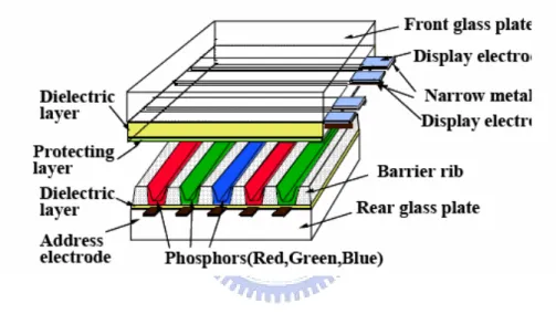
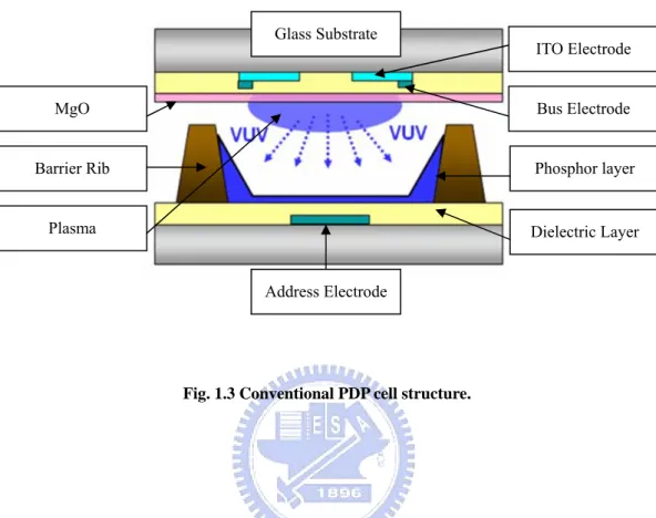
Fig. 1.3 illustrates the schematics of a PDP cell. Typical PDP has a strip of electrodes for each horizontal row of plasma cells. Pixels are separated by barrier ribs
and each of them is composed of three gas-filled cells or sub-pixels (Each cell, or pixel, actually consists of one red, one blue and one green sub-pixel).
Glass Substrate MgO Barrier Rib Bus Electrode ITO Electrode Phosphor layer Dielectric Layer Plasma Address Electrode
Fig. 1.3 Conventional PDP cell structure.
In the mass production line, conventional barrier ribs are fabricated by sandblasting method and the formation of barrier ribs is the key factor to make high
resolution plasma TV. Three primary color phosphor materials for red, blue, and green colors are deposited in the neighboring channels made by the barrier ribs to cover
both of the side wall of the ribs and the dielectric layer. Generally, phosphor materials are (Y.Ga)BO3:Eu for red; BaMgAl14O23:Eu for blue; and Zn2SiO4:Mn for green and
deposited on the barrier ribs by screen printing method.
The substrates are assembled onto each other with about a 120 µm gap and the
Ne + Xe gas mixture is introduced between each gap. A grid of electrodes deposited on dielectric layer applies an electric current to the individual cells, causing the gas in
the selected cells to ionize plasma. In order to prevent the damage caused by ion bombardment, Magnesium Oxide (MgO) plays an important role as a protective layer
is deposited on the dielectric layer.
In a word, electricity sent through an array of electrodes that are in close
proximity to the cells, excites the gas. This ionized gas (plasma) emits high-frequency VUV rays (147 and 173 nm) resulting in a discharge of ultraviolet light. The light then
strikes a phosphor coating on the inside of the glass, which causes the emission of red, blue or green visible light. The three colors in each pixel combine according to the
amount of electric pulses fed to each sub-pixel, (which varies according to the signals sent to the electrodes by the plasma display’s internal electronics), to emit visible light
1.3 Motivation and Objectives
As illustrated in Fig. 1.4, in order to protect the dielectric layer from the ion
bombardment, Magnesium Oxide (MgO) as a protective layer becomes the critical material due to its exposure under the plasma in the cell. Electron-beam evaporated
MgO films are usually used as the protecting layer for its high surface resistivity, high secondary electron emission coefficient (γ), good transparency, and strong sputtering
resistance…etc. [4-6] The secondary electron emission coefficient of the MgO film is defined as the total number of ejected electrons per incident ion and is one of the
important parameters that affect the firing and sustain voltages of an ac PDP [7]. As a result, it is believed that the performance of PDP is strongly influenced by the surface
characteristics of MgO thin films because the film is exposed to the plasma.
Fig. 1.4 The ionized gas discharge (plasma) generates vacuum ultraviolet (VUV) to stimulate the phosphor layer and emit visible light through the front panel. As shown in the figure, ion bombardment would reach to the dielectric layer which is protected by MgO [4].
deposition parameters are designed particularly to investigate the relationship between MgO thin film properties and PDP panel performance. During the fabrication process,
evaporation parameters including oxygen flow rate, electron beam current, chamber temperature, chamber pressure and tact time are selected to realize the experiment.
Furthermore, properties of the PDP such as luminance, response time, dynamic and static margin, color temperature, CIE coordinates and image sticking phenomenon,
are characterized as a function of time by demonstrating 46 inches WVGA type AC-PDP in accelerated aging tests. Both MgO thin film surface analysis and theory
are also characterized in the following chapters.
1.4 Organization
Based on the concepts mentioned above, the objective of this thesis is to realize
how the MgO thin film properties affect the PDP performance. Moreover, the PDP working mechanism and fabrication process will also be introduced. The experimental
setup will be carried out firstly for the optimization and analyses; then, the investigation and comparison will be implemented to characterize the MgO thin film
properties. This thesis is organized to review the basic theories and previous literatures in Chapter 2. Fabrication process and measurement instrument are
described in Chapter 3. The experiments with results and discussions will be placed in Chapter 4 and following is the conclusion in Chapter 5.
Chapter 2
Principle of Plasma Display Panel
In chapter 2, the basic knowledge of PDP will be introduced, including PDP history, theory of gas discharge (plasma), fabrication process, and the key materials
adopted in plasma display panels. Furthermore, the most critical material MgO thin film as a protective layer will be particularly surveyed in the final section of this
chapter.
2.1 PDP History
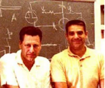
The plasma display panel was invented at the University of Illinois at
Urbana-ChampaignT (UIUC) by Donald L. Bitzer and H. Gene Slottow (shown in Fig. 2.1) in 1964 for the need for a high quality display for computer-based education, PLATO (Programmed Logic for Automatic Teaching Op-erations) Computer System
[8].
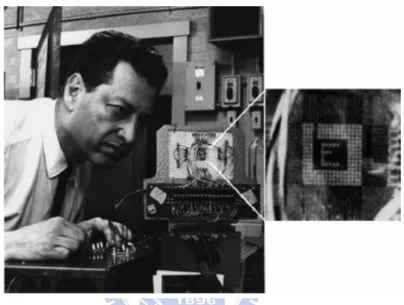
Fig. 2.1 The inventor of plasma display panel: Prof. H. Gene Slottow (left) and Prof. Donald L. Bitzer at the University of Illinois in 1967 [8].
Looking back, it was an innovating proposal at that time but may look obvious right now. In those days, the best computers adopted vacuum tubes to achieve the
desired function. The first PLATO system used a TV set and a Teletype keyboard that was connected to the University’s ILLIAC vacuum tube computer [9]. One of the key
issues of this new graphics display invention was to have inherent memory so that the bulky and expensive scan converter tube memory could be eliminated. Fig. 2.2 shows
an early plasma display as it was connected to the glass vacuum system used for the first generation. The first device used neon gas to generate the familiar neon orange
glow.
Fig. 2.2 Early plasma panel attached to the glass vacuum system at the University of Illinois. Arrow points to the 1-in by 1-in panel. This had the same alternating sustain voltage, neon gas, and dielectric glass insulated electrodes that have been widely used for PDP today [9].
Somehow, this vacuum system had a leak that a small amount of air would be
added to the neon. The solution for this situation to prevent the leakage was to add a portion of a percent of nitrogen into the neon to achieve inherent memory.
The original monochrome panels were achieved and became popular in the early 70s. Then there followed a long period of sales decrease in the late 1970s as
semiconductor memory made CRT displays relatively cheaper than plasma displays. However, IBM introduced a 19-inch monochrome display (orange on black) which
was able to show four simultaneous 3270 virtual machine (VM) terminal sessions in 1983. And late in 1992, Fujitsu announced the world's first 21-inch full color plasma
display panel. A hybrid based on the plasma display created at the University of Illinois at Urbana-Champaign and NHK STRL, achieves superior brightness and good
image quality. In 1997, Pioneer started the business selling the first plasma television in the markets. At that time (1922), screen sizes can only achieve about 21 inches.
Right now, the largest plasma display in the world shown at the CES (Consumer Electronics Show) in Las Vegas in 2006 made by Matsushita Electrical Industries
(Panasonic) measured 103-inch.
Until quite recently the superior brightness and wider viewing angle, plasma
display panels become one of the most popular forms of display for HDTV. However since that time improvements in LCD technology have closed the gap dramatically.
The lower weight, price and power consumption of LCDs have seen them make large inroads into the former plasma market.
2.1.1 Invention of Plasma Display Panel
Back to the early stage of plasma display, Fig. 2.3 shows the details of the
plasma display that appear in the original patent [10]. Basically, the fundamental concept was to insulate the driving electrodes with dielectric layers and located
between the electrodes and the neon gas mixture contained in cells. Two main issues should be notified. First of all, this is a pretty practical way to limit the current of the
gas discharge and prevent arcs. The dielectric layer could be deposited quite uniform and at low cost. Secondly, the dielectric layer could be used to store charge on the
walls, a necessary requirement for the inherent memory feature. Each pixel could store its own isolated wall charge, which allows pixels to be in either the on or the off
state even when placed along a external electrode.
Fig. 2.3 The original drawings of plasma panel from the University of Illinois at Urbana Champaign (UIUC) [10].
Fig. 2.4 shows the first plasma panel with multiple pixels. This result was first published in 1966 [11]. This was a major achievement because it was also the panel
that demonstrated the first matrix addressability [12]. The image on the panel was selectively addressed using a write pulse applied through a resistor that biased the
sustain voltage to the point where a discharge would occur. This is the first time that the inventor named this device the “Plasma Display Panel.”
Fig. 2.4 Early 4 by 4 pixel panel presented in the first publication of the plasma display panel by University of Illinois in 1966. This panel was the first to have more than one pixel [11].
In 1967, another important achievement by the University of Illinois was to develop the first color plasma panel, which is shown in Fig. 2.5 [13]. The ultraviolet
(UV) light generated by a xenon gas discharge to excite red and green phosphors was used in this project. There are three cells situated in this device, including one with a
red phosphor, a green and a non-phosphor one. All plasma TVs produced today use the UV light from xenon gas discharge exciting the phosphors in the exact same way
Fig. 2.5 First color plasma panel was this three cell prototype with red and green color phosphors excited by a xenon gas discharge. It was developed at the University of Illinois in 1967. All of today’s color plasma TVs basically generate light in this way [13].
2.1.2 Practical Commercial Structure
Accordingly, the devices developed by the University of Illinois proved that the
fundamental ideas are feasible, but they were still too fragile for public applications or commercial products. The original devices were made with three 150µm thick sheets
which were commonly used for microscope cover slips. Very thin transparent gold electrodes were placed on the surface of the outer sheets, and the inner sheet had holes
for each pixel, as shown on the right side of Fig. 2.6. On the other hand, torr-seal vacuum epoxy was adopted here to bond these three sheets together. One problem for
this arrangement is that they could not be baked to a temperature much higher than 100°C or the epoxy would decompose. As a result, leakage, breakage, and gas
contamination became the biggest issues in this condition.
In 1968, some manufacturers developed the panel shown in Fig. 2.7 having the
open-cell structure shown in Fig. 2.8. [14] This structure consists of two robust 6-mm-thick substrates made of soda-lime glass and could be fabricated in the mass
production line. The thick film electrodes made of gold with glass paste was screen printed and fired on each of the substrates and then coated with a 25 µm thick-film
lead–oxide-based solder-glass dielectric layer. This device could be baked under vacuum at 350°C to drive out contaminants and then filled with an all inert penning
gas mixture of Ne plus 0.1% Ar. This panel was strong and the gas remained pure.
Fig. 2.6 Prof. H. Gene Slottow manually addressing a 16 by 16 pixel plasma panel, developed by University of Illinois in 1967. Magnified view on the right shows the very small 1-in by 1-in panel.
Fig. 2.7 Early open-cell structure developed by Owens-Illinois in 1968. The substrate glass was 6 mm thick and the dielectric glass layers were 25 µm thick [14].
Fig. 2.8 Open-cell structure was used in this 128 by 128 pixel plasma display developed by Owens Illinois in 1968 which measured 4-in by 4-in. It consisted of a robust 6-mm-thick glass substrate, thick film gold electrodes, and a screen printed solder glass dielectric layer [14].
Later in 1968, they developed a new type consisting of 100x100 mm area and an
array of 128x128 pixels, as shown in Fig. 2.9. The front plate of this plasma display is a module for the modern PDPs. The front plate of today’s PDPs has a fundamental
structure very similar to that used for the front plate. After this very significant breakthrough, the University of Illinois continued to play an important role by
teaching to the industry the art of electronic addressing and sustaining [15]. The plasma display received significant recognition when it won the prestigious IR-100
Award in 1968. The 16x16 pixel panel shown in is the most beautiful example of the old micro-sheet panels at that time.
Fig. 2.9 16 by 16 pixel plasma display panel. The Industrial Research 100 Award was given to the University of Illinois in 1968 [15].
2.1.3 Key Features for TV Development
A. DC Plasma Displays
In the early days before PDP was invented, direct-current (DC) PDP operated by
neon negative glow had been developed for the display application. The DC- PDP was invented by Burrough Co. in the early of 1970s [16]. In those days, they used a
resister to limit the discharge current instead of the capacitor. DC-PDP had a dc discharge that acted like a shift register and addressed the individual pixels in the
panel. It had lower circuit costs due to the reduced number of external panel electrodes. They also developed a dc plasma memory method that did not require
resistors [17]. Later on, this had been used in many future prototype color displays. For many years until early 90s, there were existing two types of plasma displays. The
type that used resistor current limiting became known as the DC-PDP. The original plasma display panel that used capacitor current limiting became known as the
B. Grayscale
After successfully making plasma in the cell, how to create the desired image
becomes the next topic. However, there comes a big problem for grayscale images because a pixel was either “on” or “off.” As a result, to make a half- on state becomes
a critical issue. Unlike CRT using the electron gun to scan each line, PDP uses memory effect to gather wall charge for the ignition of plasma. The inherent memory
of PDP has advantages for making bi-level graphic displays. By the memory eddect, PDP uses wall charge to decide the “on” or “off” state of each cell. In 1972, the
grayscale problem was solved independently by Mitsubishi [18] and Hitachi. This used a technique of writing and erasing every pixel many times in a given frame so
that a grayscale could be observed based on the amount of time the given pixel was on during the frame. This driving skill is well known as the Address While Display
(AWD) method.
C. Full Color PDP
In 1978, NHK (Japanese Broadcast Corporation) as known as the most active
group for DC-PDP revealed a high-quality full-color plasma TV panel with a 16 in diagonal [19]. After that, NHK continued the work and keep a major force in the
development of color DC-PDP. This came as a natural consequence of their pioneering development of high-definition television (HDTV). NHK realized that
high resolution image looked fantastic on a large screen because the visual acuity of the eye limits the ability to see high resolution on a small screen. For this reason, they
believed that the large screen potential of the plasma display could solve this problem. However, even the future for color PDP looks very exciting in the mid 1970s, it takes
2.2 Plasma and VUV Generation
In the following pages, the basic concept and working mechanism of the
transformation from ionized gas to visible light would be introduced. PDP uses ionized gas discharge (plasma) to generate vacuum ultraviolet (VUV) to stimulate the
phosphor layer. The stimulated red, green and blue phosphor layer would emit visible light though the front panel to the human eyes. Fig. 2. 10 shows the visible light
emission process of plasma display panels.
Visible Light
Fig. 2. 10 The visible light emission process of plasma display panels. VUV is generated by plasma and is going to stimulate the phosphor layer to emit visible light.
2.2.1 Principle of Plasma Physics
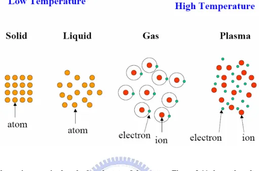
What is plasma? The central element in a fluorescent light is plasma. Plasma is known as the fourth state of matter in the universe besides solid, liquid and gas.
Basically, a gas made up of free-flowing ions (electrically charged atoms) and electrons (negatively charged particles) is identified as plasma. As shown in Fig. 2. 11,
under normal conditions, a gas is mainly made up of uncharged particles. That is, the individual gas atoms include equal numbers of positively charged particles and
electrons. The negatively charged electrons perfectly balance the positively charged protons, so the atom has a net charge of zero.
Fig. 2. 11 Plasma is recognized as the fourth state of the matter. Figure 2.11 shows the other three states in the universe includes of solid, liquid, and gas.
Plasma can be generated by introducing a lot of free electrons into the gas via establishing an electrical voltage across it. The free electrons collide with the atoms,
knocking loose other electrons. With a missing electron, an atom loses its balance. It has a net positive charge, which makes it an ion. In the plasma with an electrical
current running through, negatively charged particles are rushing toward the positively charged area of the plasma, and positively charged particles are rushing
toward the negatively charged area. Under this circumstance, particles are constantly bumping into each other with a high frequency. These collisions excite the gas atoms
into the plasma, causing them to release photons of energy. For example, xenon and neon atoms, the atoms which have been used in plasma displays release light photons
(Fig. 2. 12), which are invisible to the human eye. But ultraviolet photons can be used to excite visible light photons by stimulating the phosphor layer.
Fig. 2. 12 Where does the UV come from? Ultraviolet is emitted while a electron jumping back to the ground state of excited state.
2.2.2 Ionization and Gas Discharge
Unlike direct ionization, penning ionization is defined as the ionization that occurs through the interaction of two or more neutral gaseous species, at least one of
which is internally excited. If A* denotes an excited electronic state of atom A and B the ground electronic state of another atom (or molecule), then the process
A* + B → A + B+ + e- (2a)
is known as Penning ionization (PI), and the related process
A* + B → (A B)+ + e- (2b)
is called Associative ionization (AI). Reactions of this type have long been considered
by worker dealing with ionized plasmas, where order-of-magnitude estimates of rate coefficients have been sufficient for these purposes. If A* is metastable, however, it
may live long enough to be studied by molecular beam method [20].
Among those types of gas discharge, xenon and neon are the most popular gas
adopted in the cells for plasma display panel. Taking Xe and Ne for example, the gas discharge process can be categorized into four parts, (I) The excitement and
de-excitement of the electron impact; (II) The ionization and recombination of the electron impact; (III) Two-body heavy particle collisions; (IV) VUV radiation.
The Excitement and De-Excitement of the Electron Impact
Xe + e → Xe* + e (2-1) Ne + e → Ne* + e (2-2) Xe* + e → Xe + e (2-3) Ne* + e → Ne + e (2-4)
The Ionization and Recombination of the Electron Impact
Xe + e → Xe+ + e + e (2-5) Xe* + e → Xe+ + e + e (2-6) Xe2* + e → Xe2+ + e + e (2-7) Ne + e → Ne+ + e + e (2-5) Ne* + e → Ne+ + e + e (2-6) Ne2* + e → Ne2+ + e + e (2-7)
Two-Body Heavy Particle Collisions
Xe* + Xe* → Xe+ + Xe + e (2-8) Ne* + Ne* → Ne+ + Ne + e (2-9) Xe + Ne* → Xe* + Ne (2-10) Xe + Ne* → Xe+ + Ne + e (2-11)
2.2.3 Vacuum Ultraviolet (VUV)
As described in 2.2.2, based on the different ionization phenomenon, plasma
display panel would be able to emit visible light by the gas discharge and VUV generation first [21].
VUV Radiation
Xe2* → Xe + Xe + hυ (2-12)
Fig. 2. 13 The energy level and states of xenon gas discharge. PDP uses 147 nm and 173 nm UV light to stimulate the phosphor laer.
PDP uses the excitation and emission of the particles by emitting 147nm, 152nm and 173 nm wave length to generate the ultraviolet (UV). The energy level and states
transportation, around 30% of the energy transferred to the kinetic energy of electrons and the other 70% transferred to the kinetic energy of charged particles. Under
acceleration of electric field, the average kinetic energy of charged particles can only reach to several electron volts due to its lighter weight compared to that of electron.
This low kinetic energy of charge particle can not provide sufficient help for UV generation but transforming into heat loss. On the other hand, around 20% of the
electron kinetic energy will transform into the UV light through inelastic collision. As a result, only 6% of the imported energy will be capable transformed into the UV light
generation.
2.2.4 Photoluminescence
Photoluminescence is a process in which a chemical compound absorbs a photon
with a wavelength in the range of visible electromagnetic radiation, transitioning to a higher electronic energy state, and then radiates a photon back out, returning to a
lower energy state. The period between absorption and emission is typically extremely short, on the order of 10 nanoseconds. Under special circumstances,
however, this period can be extended into minutes or hours.
Ultimately, available chemical energy states and allowed transitions between
states (and therefore wavelengths of light preferentially absorbed and emitted) are determined by the rules of quantum mechanics. The simplest photoluminescence
processes are resonant radiations, in which a photon of a particular wavelength is absorbed and an equivalent photon is immediately emitted. This process involves no
significant internal energy transitions of the chemical substrate between absorption and emission and is extremely fast.
More interesting processes occur when the chemical substrate undergoes internal energy transitions before re-emitting the energy from the absorption event. The most
familiar such effect is fluorescence, which is also typically a fast process, but in which some of the original energy is dissipated so that the emitted light is of lower energy
than that absorbed.
An even more specialized form of photoluminescence is phosphorescence, in
which the energy from absorbed photons undergoes intersystem crossing into a state of higher spin multiplicity, usually a triplet state. Once the energy is trapped in the
triplet state, transition back to the lower singlet energy states is quantum mechanically forbidden, meaning that it happens much more slowly than other transitions.
2.3 Driving Waveform
The most popular driving waveform goes to the address display separated (ADS) method proposed by a Japanese Company Shinoda [22]. The driving waveform used
in one of the sub-fields is demonstrated in Fig. 2.14. With ADS driving method, cells are first erased by a reset step, then addressed (i.e. memory charges are deposited in
the cells which need to be ON during this sub-field), and the addressed cells are turned ON during the sustain period because the previously generated wall charges in
the address period served as priming seeds. The address and display periods are therefore clearly separated in the ADS method.
Moreover, the cells are addressed line by line. One voltage is applied to all the X electrodes. The reset period is used to erase space charges in the cell and set all the
cells to the same initial state; the memory charges are first erased, afterward, all the cells are then turned ON with a write pulse, and then erased again. Memory charges
are written on the cell when the scan pulse of a given Y electrode coincides with a pulse on the corresponding address electrode. After the cells of the whole screen have
been addressed, sustain period launches and a discharge occurs in the cells which have been addressed, at a given subfield numbers.
Fig. 2. 14 The most popular driving waveform - address display separated (ADS) method proposed by a Japanese Company Shinoda. Figure 2.14 shows the driving waveform used in one of the sub-fields
2.4 Protective Layer – MgO
Magnesium Oxide (MgO) is now fully adopted as a protective layer in the
plasma display panel. It plays a very important role in the AC-plasma display panel (AC-PDP) to protect the electrode and the dielectric material from the bombardment
of ions, electrons, photons, and metastable atoms.
The discharge voltage of an AC-PDP is largely affected by the protective layer
since the operation mechanism of the plasma display panel is based on the gas discharge phenomenon occurring around the protective layer that covers the dielectric
layer. In actual operation of PDP, a low firing voltage is required to conserve the electrical power of the driving circuit. When the AC pulse voltage is applied at some
high frequency between the discharge electrodes, and the plasma is ignited in the gas volume, the protective layer plays a role in reducing the voltage for discharge by
means of emitting secondary electrons. Thus, MgO has been used as a surface protective layer on the dielectric material in the AC-PDP. However, materials with
better electrical characteristics are needed to meet the demands of advanced high-vision PDPs with low-power consumption. Thus, many research groups have
tried to make new protective materials with better electrical characteristics than MgO. So far, many researches have been made for the development of high efficiency
dielectric protection materials including Al2O3, La2O3 and CeO2, and, it is known that
MgO is the best candidate for the dielectric protection material. Unique features such as high secondary electron emission coefficient (γ), high transparency, and good
sputtering resistance are the main reasons that give MgO such a big success till now. Bulk magnesium oxide is known as a highly ionic crystal with the Mg-O bonds
having about 80% ionic character. Generally, ionic materials have the strong bonding.
The electron induced secondary electron emission coefficient of the evaporated magnesium oxide is as high as 17, much higher compared with that of Al2O3, a value
of 3.2 [23].
In this section, MgO as a protective layer evaporated by electron beam induced
would be introduced in detail including development of PFP history, chemical profile, physical characteristics, and TV application.
2.4.1 MgO development in PDP History
In the early days, the original open cell structure was not yet optimized for the display application even though it was already very practical. The dielectric layer was
not a very suitable gas discharge cathode because the very energetic ions in the cathode fall would sputter the surface and erode the surface structure. This defect on
the surface may result in the decrease of secondary electron emission coefficient (γ), unstable discharge and varied driving and sustaining voltage. Such a voltage drift was
unbearable in the display application where one sustain voltage needed to be adjusted for all the other million pixels. Unfortunately, the voltage of the on-state pixels would
drift at a different rate than the pixels that were at off-state. The remarkable breakthrough came in 1971 with the development of the MgO protection layer
cathode.
After the dielectric layer was deposited, a 500-nm-thick layer of MgO was
deposited by electron beam evaporator on both the front and rear panel. Electron beam evaporation also becomes the general method to evaporate MgO thin film on
dielectric layer in modern PDPs. This refractory magnesium oxide helped the voltage condition became quite stable in the life test. The key features consist of very high
ion-induced secondary electron emission and a very low sustain voltage. It was believed that the MgO protective layer for plasma displays was independently
invented at three different companies: IBM, Owens-Illinois, and Fujitsu [24]. The first PDP products with MgO were developed in October of 1973 by IBM. [25].
Arguments were made in U.S. courts for many years in order to decide which company invented MgO for the plasma display application. Ultimately, the courts
awarded the MgO patent to Owens-Illinois.
2.4.2 Chemical and Physical Profile
Magnesium is a silvery white metal. The surface of magnesium metal is covered
with a thin layer of oxide that helps protect the metal from attack by air. Once ignited, magnesium metal burns in air with a characteristic blinding bright white flame to give
a mixture of white magnesium oxide, MgO, and magnesium nitride, Mg3N2.
Magnesium oxide is more normally made by heating magnesium carbonate. Calcium,
immediately below magnesium in the periodic table is more reactive with air than magnesium.
2Mg(s) + O2(g) → 2MgO(s) (2-12)
3Mg(s) + N2(g) → Mg3N2(s) (2-13)
Magnesium oxide has an empirical formula of MgO. It is a white solid mineral that occurs naturally as periclase and is a source of magnesium. Periclase is
sometimes used as a gemstone although it lacks good hardness and is generally limited in colors. Periclase is relatively scarce and is found in marbles being formed
from the dissolution of dolomite, CaMg(CO3)2 , into MgO-periclase, CaCO3and CO2.
MgO is widely used as a sport for absorption and growth of different materials,
such as metals, semiconductors, superconductors and optoelectronic devices. It is also used as a catalyst for heterogeneous reactions. It is formed by an ionic bond between
one magnesium atom and one oxygen atom. MgO (sometimes called magnesia) is formed commercially by heating magnesite to 600-800 °C, which drives off most of
the CO2. It has good thermal conductivity and electrical resistivity at elevated
temperatures. Following catalogs the general description of MgO:
Magnesite - A mineral composed of MgCo3.
Magnesite Grain - dead-burned magnesia in granular form in size suitable for
refractory purposes.
Seawater Magnesite - Dead-burned magnesia made by a chemical process using
seawater or other solutions (brines).
Table 2.1 shows the fundamental chemical and physical properties of MgO. Usually MgO is composed of single crystals, pieces, targets, and powder sized as fine
as nanometers. The theoretical composition of magnesite is around: MgO= 47.8% and Co2= 52.2%.
Table 2.1 The chemical and physical profile of MgO.
2.5 Summary
The introduction to PDP history and fundamental working mechanism are
introduced in this Chapter. Literature surveys point out the key features and state the critical issues of plasma display panels. Among those features and characteristics,
MgO thin film as a protective layer is considered as one of the most important issues. In the following chapter, experimental setup will be designed to modify the effect of
MgO thin film on PDP performance. E-Beam evaporation would be adopted to deposit the MgO thin film on the dielectric layer. Flow of fabrication process would
Chapter 3
Fabrication and Measurement Instrument
Plasma display panels (PDPs) can be made in large sizes and are expected to be the best candidates for wall-mount displays that are too big to be made using CRTs
(i.e., 40-inch and larger). However, broadcasting of high-definition TV (HDTV) will start when digital TV broadcasting begins, and resolutions exceeding one million
pixels will be required even for standard TV units.
3.1 Introduction
The markets for large area PDPs larger than 40 inch diagonal size have been
expanded rapidly. The large area flat panel display is demanded for a HDTV and a digital TV which displays a real and life-size image in addition to the traditional TV
image because of the development of the both computer and network technologies. This propagation includes the three-color PDP in 1989, the 21-inch diagonal color
PDP with 260 thousand colors in 1993, and the 42 inch diagonal full color PDP with 16.7 million colors in 1996. These results have opened the dream of a wall hanging
TV. Looking back a history of color PDP, a development of the 21 inch PDP was the most important step in which the most essential technologies for large area PDPs have
been completed. The commercialized 42 inch and 50 inch PDPs have been developed based on several technologies [26-29]. This chapter will describe the manufacturing
technologies for modern color PDPs in the markets.
Before introducing the flow of PDP fabrication process, fundamental PDP
structure would be reviewed firstly. The practically developed T-shaped PDP structure is shown in Fig. 3.1. Paired parallel display data electrodes, sustain electrode
X and scan electrode Y, are formed on the front glass substrate. Each display electrode is composed of a transparent SnO2 (ITO) and a narrow bus electrode of
multi-layered Cr, Cu and Cr. They are capable to emit a luminance effectively through the transparent electrode and reduce the electrode resistance. These electrodes
are covered with a dielectric layer which is made of low melting glass materials. This layer is covered by another protective layer-MgO thin film. Besides, striped address
electrodes A are arranged on the rear substrate.
Fig. 3.1 The typical T-shaped structure which has been widely used in PDP products.
Striped type barrier ribs are on both side of the address electrodes to separate the
adjacent discharge cells and to eliminate the optical cross-talk between each cell. Three primary color phosphor materials for red, blue, and green colors are deposited
in the neighboring channels made by the ribs to cover both of the side wall of the ribs and the dielectric layer. The structure has realized good performances such as a high
luminance, a high luminous efficiency and a wide viewing angle.
Phosphor materials are BaMgAl14O23:Eu for blue, (Y.Ga)BO3:Eu for red,and
µm gap. A Ne + Xe gas mixture is introduced between the cell gap. The fabrication
process is also simple enough to mass-produce so the PDP has advantages such as a
low cost process and easiness to manufacture large area panels and high resolution panels.
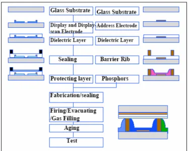
3.2 Fabrication Process of Plasma Display Panel
Figure 3.2 shows the basic PDP fabrication process flow chart. First of all, the front plate process would be introduced. The transparent conductive ITO film is deposited onto the front glass panel. The multiple paired data electrodes are deposited
by photolithography technology. As shown in the figure, the metal electrode film consists of a Cr/Cu/Cr multi-layer is sputtered on these transparent ITO electrodes.
The bus electrode is also formed by photolithography technology. Besides, these electrodes are covered by a frit glass layer with screen printing method and then fired
to about 600° C to turn out the dielectric layer. The seal glass layer with a width of about 3 mm is adhesive surrounded outside the display area with a pre-firing process.
Additionally, MgO protective layer is evaporated on the dielectric layer over the display area of inside of the seal layer.
Following are the rear plate fabrication processes. A small hole of a diameter of about 1 mm is drilled on a corner of the rear plate. The Ag address electrodes are
printed and fired. The frit glass is printed on the electrodes in the display area and then fired about 600° C to form the dielectric layer. The barrier ribs are made by
sandblasting the frit glass on both sides of the address electrodes and then fire. The red, green, and blue phosphors are printed inside of the channel between the barrier
ribs. Each color phosphors are printed simultaneously and repeated three times, and then dried. The rear plate is completed with these processes.
Both front and rear plates are assembled and fixed with clips. The assembled plates are fired to melt the seal layer and the plates are glued to integrate the panel.
For the gas filling process, the panel is connected to an evacuation gas-filling system through the evacuating glass tube. After the baking step, the discharge gas mixture is
then filled in. Finally, the whole PDP fabrication is completed after cutting off the evacuating tube. The driving pulse is applied to the panel and discharges are ignited in
every discharge cells to reduce and make stable the operating voltage, which is known as the aging process.
3.2.1 Front Plate Fabrication I. Glass Substrate
The most famous glass substrate company in PDP business goes to Asahi Glass
Co., Ltd. It is reported that the number of PDP television sets is forecast to rise to 9 million units in 2007 from 1.4 million units in 2003, demonstrating annual growth of
60% during this period.
Asahi Glass started its PDP glass substrate production in 1996 at the Kansai
Plant, becoming the world's pioneer in the field, and since then the Company's PD200 model has become a de facto standard. The PD200 now accounts for 90% of the
global market for PDP glass substrate products. This glass substrate material for PDP has been developed to prevent the distortion and the shrinkage of the glass substrate in
the firing processes of high temperature. The high strain point glass has about 100° C higher strain point comparing to the conventional soda-lime glass. This eliminated the
distortion and reduced the shrinkage in the process and then made it possible to construct the process with a large process margin.
II. ITO Electrode
The ITO (Indium Tin Oxide) or SnO2 is designed for the use in AC-PDP. It is
used for a transparent electrode in the front panel in order not to block the light
transmission. ITO has excellent conductivity and good transparency but worse heat and etching resistance. Fig. 3.3 illustrates the processes for ITO and SnO2 formation
in the front panel fabrication.
The ITO film is made by a sputtering or an ion- plating method. It is patterned by photolithography processes. A photo resist is usually coated with a roll-coating
machine because of it’s the large area. The expose uses a proximity method with a vertically supporting mechanics to prevent the bending of the glass substrate. As an
exchange of a large photo mask is also a big issue, so the direct exposure machine is developed and practically used. The ITO film is etched with a solution of
hydrochloric acid with small amount of nitric acid. The performances of the conductivity, transparency, etching ability, the adherence with Cr, resistance to the
etching solution of Cr and resistance to the reaction with the dielectric layer while firing should be concerned to optimize an ITO films. Although SnO2 has advantages
on the stability of the film quality and conductivity over ITO, the etching parameters and conditions are too difficult to control. The film is now patterned with the liftoff
process with heat resistant photo -resist.
III. Bus Electrode
Bus electrode is also known as auxiliary electrode. Since alarming heat would be
released during the gas discharge and lead to the increasing resistance of transparent electrode, bus electrode is used to reduce the electric resistance of the transparent
display electrodes. Ag and Cr/Cu/Cr are currently used to be the bus electrode. An Ag electrode is made with a printing method or a photolithography with photosensitive
paste including Ag and frit glass as shown in Fig. 3.4. The Cr/Cu/Cr is made with sputtering method and patterned with photolithography method. Bus electrode is
contributive to control and stabilize the gas discharge and enhance the conductivity, so it is considered as an auxiliary electrode.
Fig. 3.4 An Ag electrode is made with a printing method or a photolithography process with photosensitive paste including Ag and frit glass [30].
IV. Dielectric Layer
Dielectric layer has good voltage resistance and is able to capture charges to achieve the memory effect. Dielectric layer is made by forming the layer of the low
melting frit glass composed of and then fired at about 600° C to make transparent glass layer. It is important to make a uniform dielectric layer in the PDP fabrication
process. The dielectric layer of a front substrate should have high transparency due to affect to the display performance. There are some methods to make the frit glass layer, such as screen-printing, slot coating, roll coating, and green sheet [30]. The most
common method is screen-printing and shown in Fig. 3.5.
The glass layer is made by the way that the paste including frit glass and organic solution is deposited on the substrate through the mesh of screen. It is important to
keep a sufficient time for leveling after printing to eliminate the roughness due to the mesh because the thickness uniformity affects on the differences in the discharge
voltage of the cells. Beside screen printing method, two technologies are introduced. The slot coating method is the way that the glass paste is deposited through the slot of
thickness around 10 µm. The roll coating method is the way that once the layer of a paste is made on the roll and then transcribed on the substrate. Both methods do not
use the screen mesh. There however remains an issue of that if the drying condition is controlled insufficiently, the uniformity is not adequate and the crack of the layer
appears. The green sheet method is the way that a dried layer made on the base film is put on the substrate and then fired. Although this also realizes a good uniformity, a
sufficient degas while firing is required because much organic binder is included in the glass film.
Fig. 3.5 Screen printing method [30].
V. MgO Protective Layer
It is believed that the protective layer is the one of the most key element to realize a good performance. At the early stage of PDP development, even though a lot
of materials were investigated for the protection function, but MgO was then found to be the most appropriate material for a protecting layer [31]. Other materials were
never successful because MgO combines several unique characteristics. The performances requested for the protecting layer includes high secondary electron
emission, high sputtering resistance, high transparency, non-conductivity, high stability in the PDP fabrication processes
As a result, MgO becomes the most appropriate materials for these requirements. For the mass production, MgO layer is usually formed by electron beam evaporation
method. E-beam evaporation can provide stable result and the cost is quite acceptable. There are several new methods have been investigated in order to achieve more
efficiently production, such as ion plating, reactive sputtering, plasma treatment, etc.
3.2.2 Rear Plate Fabrication I. Address Electrode
The address electrode process is almost same as the bus electrode in the front plate process. Since address electrode is located in the rear plate, there is no need to
be transparent. Ag is currently adopted for the address electrode material. An Ag electrode is made with a printing method or a photolithography with photosensitive
paste including Ag and frit glass. Just like bus electrode, address electrode is contributive to control and stabilize the gas discharge and enhance the conductivity.
II. Barrier Ribs
Barrier ribs are arranged and located to a spacer supporting front panel and separating each cell. The formation of barrier rib is one of the most unique processes
in PDP fabrication and significantly effect could be seen on the cost. The thickness and width of the rib is around 150 µm and 70 µm, respectively. Although the printing
technologies were used at first to make barrier ribs, the sandblasting method then took over due to the accuracy formation and excellent structure shape.
The sandblasting has advantage to get the high accurate barrier rib due to use the photolithography. Fig. 3.6 shows the process for sandblasting method. A thick frit
glass layer is formed on the display area, and then covered with a dry photo-sensitive elastic film. The film is exposed through the film with barrier rib pattern and then
developed. The small hard particles are then sprayed out in a high pressure. Even though the frit glass layer of the area without elastic layer is cut, the area of the layer
coated by the elastic film is remained because the particles would be reflected.
Fig. 3.6 Typically sandblasting method used to form the barrier ribs [30].
As shown in Fig. 3.6, the covered film is removed and then fired to complete the barrier ribs. The subject of the sandblasting process is that the 70 % of the materials
formed on the plate are thrown away finally and then material cost is expensive. The recycle system of the material should be developed. In the photosensitive paste (PS)
method, the thick PS layer composed of photosensitive material and frit glass is used. As the glasses in the PS layers reflect and disturb to make accurate barrier rib, thick
layer is not possible at once. The processes of formation of PS layer and exposition are repeated two or three times and then fired to form the barrier rib.
III. Phosphor Layer
While depositing phosphor on the barrier ribs, it is important to prevent the cross
printing. The printing method for phosphor layers is shown in Fig. 3.7. It is the most practical and efficient method so far in the industry. The phosphor formation process
is unique because the phosphor layer is deposited on the barrier ribs and sidewall inside of the channel. The required tolerance of the phosphor deposition with the
printing is not severe comparing to the printing processes for electrodes and barrier rib. That is because that as the phosphor paste is filled in the channel through the
screen, the pattern of the screen can be designed narrower than the channel width. The filled paste is then dried. The drying condition is important to make uniform phosphor
layers. The thickness of the phosphors can be determined by the composition of the phosphors in the paste. The phosphor layer deposited is shown in Fig. 3.8.
Fig. 3.8 Phosphor layer on the barrier ribs with red, green, and blue color [30].
3.2.3 Panel Assembling
After the front and rear panel process, it needs assembling, evacuation and gas filling to complete the whole fabrication process. The front and rear plates are
assembled to align the display electrodes and address electrode in orthogonal. As shown in Fig. 3.9, the plates are pre-fixed with clips. The evacuating tube is placed on
the hole with the frit paste and PCB. After the assembling, it is fired about 400° C to glue the plate each other by melting the seal layer. The panel is connected with an
evacuation and gas filling system through the evacuating tube. The panel is placed inside of the furnace and baked out about at 350° C to evacuate the adsorbed gases on
the surface of MgO, phosphors, barrier ribs and dielectric layers. After the sufficient baking, the panel is cooled down to the room temperature and then discharge gas is
introduced to the designed pressure. Finally, the PDP is completed after cutting off the evacuating tube. As this process is one of the most important processes to decide
the characteristics of PDP, the temperature while evacuation, evacuation system without impurity, and purity of filling gas should be controlled carefully. After the
assembling, aging test is required to stabilize the panel discharge condition in order to provide normalized panel performance.
Fig. 3.9 Assembling process of front panel and rear panel. It needs to fire up to 400 degree C to seal the panel [30].
3.3 Experimental Setup
It is believed that PDP performance is strongly influenced by the surface
characteristics of MgO thin films because the film is exposed to the plasma directly. Gas discharge and ion bombardment would sputter the surface structure and affect the
panel properties. In this study, the deposition parameters are optimized and the relationship between the density of the MgO films and the properties of the AC-PDP
is investigated. The influence of MgO density and surface morphology on panel properties has been examined with a accelerated life aging test.
The experiments in this study have been carried out to characterize the properties of twelve, 46-inch WVGA type plasma display panels. In order to characterize the
effect of MgO thin film on PDP panel performance, several parameters would be chosen to make different formation MgO thin films. The experimental PDP modules
are fabricated by ChungHwa Picture Tube (CPT) Co.
Table 3.1 The evaporation parameter of MgO thin film by E-Beam evaporation in this study.
MgO thin film as a protective layer in experimental PDP modules were deposited by electron beam evaporation. The deposition parameters are categorized in Table 3.1.
sccm), and electron beam current (550, 600, 650 mA). Moreover, different film thickness (5000, 7500, 10000 Å) were selected to examine the experiments and the
temperature in the chamber during the evaporation is controlled from 220 to 240˚C. After the panel fabrication, the bonding process required to attach the specific
driving circuits on the back of rear panel. Afterward, each experimental PDP module was operated in an accelerated aging environment. In this study, the aging process
requires a frequency three times higher than the conventional driving waveform and all of the panels were operated continuously prolonged to 1500 hours for the data
recording.
Generally, the conventional PDP manufactured by CPT uses 40 sccm O2 flow
rate and 600 mA electron beam current to form a 7500 nm thick MgO thin film. Accordingly, the evaporated parameters were designed to investigate the details and
panel properties difference between conventional ones and experimental ones. It is believed that varied oxygen flow rate during the Mg and O atom formation can
change the stoichiometery of the MgO thin films [32-34]. We believe that this change
can be a very key rule to the panel performance. Unlike bulk MgO, MgO thin films
formed with different evaporation condition can also provide different thin film density, which is also a key element to affect the panel properties. Additionally, the
change of evaporation parameters can also influence the surface morphology of MgO thin film. By the atomic force microscopy (AFM), surface morphology of MgO thin
film would be characterized. Another thing to affect the MgO performance is the crystallinity of the thin film. Stronger crystal structure may guarantee lower sputtering
rate against the ion bombardment. Therefore, X-ray diffraction (XRD) would be adopted to investigate the crystallinity of MgO thin films. All the detail experimental
![Fig. 2.3 The original drawings of plasma panel from the University of Illinois at Urbana Champaign (UIUC) [10]](https://thumb-ap.123doks.com/thumbv2/9libinfo/8094845.164819/23.892.229.696.552.940/original-drawings-plasma-panel-university-illinois-urbana-champaign.webp)