國立交通大學
電子工程學系 電子研究所碩士班
碩士論文
以金屬誘發側向結晶之多晶矽薄膜電晶體
的製作與分析
Fabrication and Analysis of Poly-Si TFTs Made by Metal
Induced Lateral Crystallization Technology
研 究 生:王偉銘
指導教授:林鴻志 博士
黃調元 博士
以金屬誘發側向結晶之多晶矽薄膜電晶體
的製作與分析
Fabrication and Analysis of Poly-Si TFTs Made by Metal
Induced Lateral Crystallization Technology
研 究 生:王偉銘 Student: Wei-Ming Wang 指導教授:林鴻志 博士 Advisors: Dr. Horng-Chih Lin 黃調元 博士 Dr. Tiao-Yuan Huang
國立交通大學
電子工程學系 電子研究所碩士班
碩士論文
A Thesis
Submitted to Department of Electronics Engineering & Institute of Electronics College of Electrical and Computer Engineering
National Chiao-Tung University in Partial Fulfillment of the Requirements
for the Degree of Master in
Electronic Engineering July 2008
Hsinchu, Taiwan, Republic of China
以金屬誘發側向結晶之多晶矽薄膜電晶體的製作與分
析
研究生:王偉銘 指導教授:林鴻志 博士 黃調元 博士國立交通大學
電子工程學系 電子研究所碩士班
摘 要
在本篇論文中,我們對以金屬誘發側向結晶製程(MILC)之多晶矽薄膜電晶 體(Poly-Si TFT)進行研究。首先在材料分析部分,我們量測並分析了薄膜厚度、 製程溫度與金屬引洞尺寸對 MILC 製程的影響,並運用光學與電子顯微鏡對 MILC 實際長度與薄膜結構進行分析。而在實際元件製作部分,我們用兩種不同 製程製作 MILC TFT 以分析製程的不同對元件特性的影響,並與固向結晶法(SPC) 製作之 TFT 進行比較,而同時,我們也研究了元件尺寸對 MILC Poly-Si TFT 電 性的的影響。最後,我們利用本實驗室發展出的特殊結構 HC-TFT 對離 MILC 金 屬引洞不同位置的 MILC 薄膜的電性進行分析,並萃取其汲極漏電流的活化能 (Ea)以及狀態密度(DOS)做進一步的分析。Fabrication and Analysis of Poly-Si TFTs by Metal
Induced Lateral Crystallization Technology
Student: Wei-Ming Wang Advisors: Dr. Horng-Chih Lin Dr. Tiao-Yuan Huang
Department of Electronics Engineering & Institute of Electronics National Chiao-Tung University
Abstract
In this thesis, we investigate the material and electrical properties of poly-Si
TFTs prepared by metal induced lateral crystallization (MILC) process. The relations between MILC length and film thickness, process temperature, and the dimensions of MILC seeding window were measured and discussed. The OM and SEM pictures after secco etching were used to probe the MILC length and film structure. Poly-Si TFTs fabricated by two kinds of MILC processes as well as SPC process were analyzed and compared. Characteristics of MILC TFTs with various dimensions were characterized to understand the impact of geometrical parameters of the device structure in affecting the device performance. We also employed a novel tester named HC-TFTs to resolve the location dependence and impact of the MILC poly-Si film on device characteristics. Finally, the characteristics of these TFTs, such as transfer characteristics, density of states (DOS), and the activation energy of leakage current (Ea), were also measured and discussed.
Acknowledgement
終於畢業了,從一開始充實基本知識,到實際實驗與元件的量測與分析,歷 經 3 年的時間,該感謝的人多不勝數。首先要感謝林老師與黃老師三年來的指 導,在每次 group meeting 時對我的啟發以及指導我完成學業,以及對我研究方 向與內容的討論,特別是最後的論文,對英文不好的我來說英文論文真是一大挑 戰,但是對老師來說,不僅要改我的文法又要猜測我的文意,並在我每次修改後 不厭其煩的幫我修飾,老師,真是辛苦您了,也謝謝您了。 再來要感謝的則是學長們,對一個八竿子打不著的電信系畢業的我來說,沒 有學長們的指導我大概無法適應與磨合電子所應具備的基礎知識。特別是阿賢學 長以及 Benson 學長,常常大半夜的陪我 training 機台、陪我做實驗、以及幫我 分析 data,勞苦功高,但我卻幫不了你們什麼,只能在這裡謝謝你們。再來則 是要感謝同學們,對起步較晚的我來說,同學們的幫助有如雪中送炭。特別是子 儀,在同學們都畢業後就只剩他繼續唸博士,所以不論是實驗亦或是在論文上都 受其幫助甚深,而更是生活娛樂上的好伙伴。 再來則是要感謝好學弟們,對延畢一年的我來說,你們與其說是學弟,還不 如說是朋友比較合適,大家一起研究 Data,一起到處吃好料的,一起聊一些沒營 養的東西,令我求學的最後一年也過的相當愉快,謝謝你們;而其中,要特別感 謝小強,作為同組的學弟,因為研究方向相近,你的許多實驗數據以及論點都對 我有相當大的啟發,而在我論文中的許多研究也都是在你的幫助下才完成的,而 今年大家也要一起畢業了,除了感謝你們之外,也祝福你們之後服役順利,將來 能找到好工作。 當然,沒有家人的支持我也無法如此無後顧之憂的完成學業,長年在外打拼 的老爸、從小擔心我到大的老媽,謝謝你們!當然還有老哥,作為兄長真的相當 稱職,謝謝你的生活費,以及,祝你新婚快樂。 王偉銘 2008.07.21 新竹Contents
Abstract(Chinese)………...………..i Abstract(English)………...………..ii Acknowledgement(Chinese)………...iii Contents………...iv Table Captions……….vi Figure Captions………...…...vii Chapter 1 IInnttrroodduuccttiioonn…………………………………………………………………………………………………………………………..1 1 1-1 General Background of Poly-Si TFT………...………11-1.1 Solid Phase Cristallization….………...1
1-1.2 Metal Induced Lateral Crystallization………...2
1-1.3 Excimer Laser Crystallization………...3
1.2 Motivation………....4
1.3 Organization of This thesis………...………....4
Chapter 2 Material Preparation, Device Fabrication and Measurement Setup.6 2-1 Material Preparation……….………6
2-2 Device Fabrication……….………..6
2-2.1 Type-A device fabrication……….6
2-2.2 Type-B device fabrication……….7
2-3 Hot-carrier (HC) TFT Test Structure…...……….8
2-4 Measurement Setups for Electrical Characterization………..……….8
3-1 Material Characterization………...10
3-1.1 Effects of channel (film) thickness………....………….10
3-1.2 Effects of MILC window width………..…………11
3-1.3 Temperature effects to MILC……….……….12
3-2 Characteristics of MlLC Poly-Si TFTs Fabricated with Type-A Process……..…12
3-2.1 Effects of Channel Length………..12
3-2.2 Effects of MILC Seeding Window Arrangement………14
3-2.3 Effects of Channel Width………....15
3-2.4 Effects of Source and Drain Terminal Arrangement………..….16
3-2.5 Comparisons of One- and Two-Step Annealing……….…….16
3-2.6 Ammonia Plasma Treatment………...…………17
3-3 Characteristics of MILC Poly-Si TFTs Fabricated with Type-B Process…….….18
3-3.1 Effects of Channel Length………..19
3-3.2 Effects of Channel Width………...………….20
3-3.3 Ammonia Plasma Treatment………..………….21
3-4 Leakage Mechanisms……….…………22
3-5 Characteristics of HC-TFTs………...……24
3-5.1 HC-TFTs for Large Scale Devices (BE1_1)……….……..24
3-5.2 HC-TFTs with Small Dimensions (BA1 and BB1 splits)………...…………26
Chapter 4 CCoonncclluussiioonn…………………………………………………………………………………………………………………………....2299 4-1 Conclusion……….………29
TABLE CAPTIONS
CHAPTER 3
Table 3.1 Major electrical parameters extracted from the transfer curves measured at Vd =0.1V in Fig. 3.6. Definition of the Effective (Eff) Vd is given in Eq.3-1 ..……….………….………..………...………44
Table 3.2 Major electrical parameters extracted from the transfer curves measured at Vd = 0.1 V in Fig.3.14………..……...………..………...………49
Table 3.3 Major electrical parameters extracted from transfer curves measured at Vd = 0.1 V in Fig. 3.22. Definition of the Effective (Eff) Vd is given in
Eq.(3-1)……….……..………...……...54
Table 3.4 Major electrical parameters extracted from transfer curves measured at Vd = 0.1 V in Fig.3.27(a)...58
Table 3.5 Major electrical parameters extracted from transfer curves measured at Vd = 0.1 V in Fig.3. 29………...…….59
Table 3.6 Major electrical parameters extracted from transfer curves in Fig.3.30 ……..……….…60
Table 3.7 Major structural parameters of HC-TFT. (unit: um)………...……….……63
Table 3.8 Major electrical parameters extracted from the transfer curves in Fig. 3.34 and Fig. 3.35………..……….…..65
FIGURE CAPTIONS
CHAPTER 2
Fig. 2.1 Material Preparation………....….…...………..35
Fig. 2.2 TFTs fabrication (type A)...………..………...………..36
Fig. 2.3 TFTs fabrication (type B)……….……….………..………..38
CHAPTER 3
Fig. 3.1 Observed MILC length as a function of time. Thickness of the Si films is 50 nm or 100 nm………....40
Fig. 3.2 MILC length as a function of open window size. The sample was annealed at 550℃ for 24 hours……….41
Fig. 3.3 Schematic model for the explanation of MILC window size effect……..41
Fig. 3.4 MILC length as a function of annealing time with seeding window size as parameter for two different annealing temperatures………..42
Fig. 3.5 An exemplary layout for devices used to investigate the effect of channel length on device performance. Major dimensional parameters are also illustrated.………...43
Fig. 3.6 Transfer characteristics of MILC TFT (Type-A) at Vd=5V and 0.1V with various channel length. The channel width is 20um………..43
Fig. 3.7 Re-plot of Fig. 3.6 normalized to channel length………..44
Fig. 3.8 Measured total device resistance R versus drawn channel length L of MILC TFTs (Type-A) with only one MILC open window at source region. Channel width W is 20 um……….…45
Fig. 3.9 Measured total device resistance R versus drawn channel length L of SPC poly-Si TFTs with S/D activation steps same as MILC devices in Fig. 3-8……….……..45
Fig. 3.10 MILC TFTs with (A) one-side and (B) two-side MILC open window arrangement………....46
Fig. 3.11 Transfer characteristics of MILC TFTs (Type-A) with one-side and
two-side MILC open windows………..…….46
Fig. 3.12 Measured total channel resistance R versus drawn channel length L of MILC TFT (Type-A) with two-sided MILC open windows. Channel width of the device is 20 um………47
Fig. 3.13 An exemplary layout for devices used to investigate the effect of channel width on device performance. Major dimensional parameters are also illustrated………...…….47
Fig. 3.14 Transfer characteristics of MILC TFT (Type-A) with various channel width but identical channel length of 2um……….48
Fig. 3.15 Normalized transfer characteristics of MILC TFTs (Type-A) with various channel width but identical channel length of 2um………48
Fig. 3.16 Transfer characteristics of a MILC TFT (Type-A, L/W=10um/20um)under forward and reverse modes of measurements………...….49
Fig. 3.17 Transfer characteristics of MILC TFTs (Type-A, L/W=10 um/20 um) processed with one- and two-step S/D anneal………...…….50
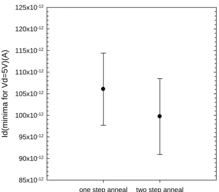
Fig. 3.18 Distribution of minimum drain current at Vd=5V for devices with one- and two-step S/D anneal………...…..50
Fig. 3.19 Distribution of minimum drain current at Vd=5V and Vg = 20V for
devices with one- and two-step S/D anneal………..…..51
Fig. 3.20 Distribution of subthreshold swing at Vd=0.1V for devices with one- and two-step S/D anneal………..….51
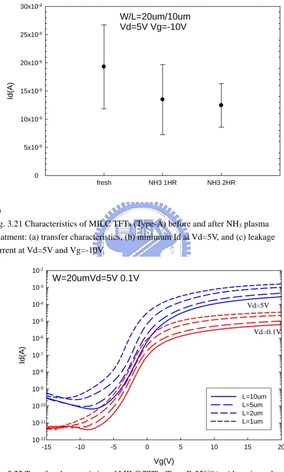
Fig. 3.21 Characteristics of MILC TFTs (Type-A) before and after NH3 plasma
treatment: (a) transfer characteristics, (b) minimum Id at Vd=5V, and (c)
leakage current at Vd=5V and Vg=-10V………...….52
Fig. 3.22 Transfer characteristics of MILC TFTs (Type-B 550℃) with various channel length but identical channel width of 20um. Vd=5V and
0.1V………...….53
Fig. 3.23 Transfer characteristics of MILC TFTs (Type-B) shown in last figure normalized with the channel length………...……….54
Fig. 3.24 Measured total device resistance R versus drawn channel length L of MILC TFTs (Type-B) with only one MILC open window at source region. Channel width W is 20 um……….55
Fig. 3.25 Measured total device resistance R versus drawn channel length L of SPC TFTs which received the same S/D annealing treatment as MILC process Type-B………56
Fig. 3.26 Transfer characteristics of SPC poly-Si TFTs normalized with the channel length………..………56
Fig. 3.27 (a) Transfer characteristics for MILC TFTs (Type-B) with various channel width but identical channel length of 2um (b) Transfer characteristics of the devices normalized with the channel width……….……….57
Fig. 3.28 Illustration of the appearance of parasitic channels on the sidewall of the active layer……….58 .
Fig. 3.29 Transfer characteristics of SPC poly-Si TFTs normalized with the channel width………..…….58
Fig. 3.30 Transfer characteristics of Type-B devices with and without plasma
treatment……….……60
Fig. 3.31 Activation energy of MILC TFTs: (a) Type-A under forward and reverse modes of measurements, (b) Type-B under forward and reverse modes of measurements, and (c) comparisons of the three types of devices……….61
Fig. 3.32 Transfer characteristics of Type-A, Type-B, and SPC TFTs………..62
Fig. 3.33 Schematic of HC-TFT test structure……….….63
Fig. 3.34 Transfer characteristics of the main transistor in a HC device (BE1_1) under forward and reverse modes of measurements………..64
Fig. 3.35 Transfer characteristics of the three monitor transistors in a HC device (BE1_1)………..…65
Fig. 3.36 Activation energy of leakage current for the three monitor transistors in a HC-TFT device (BE1_1)………..……..66
Fig. 3.37 Extracted density-of-states for the three monitor transistors in a HC-TFT (BE1_1)………..……67
Fig. 3.38 SEM pictures after Secco etching taken in the channel regions of (a)ST, (b)MT and (c)DT in a HC-TFT (BE1_1)………..………….67
Fig. 3.39 Transfer characteristics of the main transistor in a HC device (BA1) under forward and reverse modes of measurements………...…….70
Fig. 3.40 Transfer characteristics of the three monitor transistors in a HC device (BA1)……….…….70
Fig. 3.41 An OM picture of the MILC region near a 5umX10um MILC seeding window after annealing at 550℃ for 24Hr………71
Fig. 3.42 Activation energy of leakage current for the three monitor transistors in a HC-TFT device (BA1)………..….72
Fig. 3.43 Transfer characteristics of the main transistor in a HC device (BB1) under forward and reverse modes of measurements………...….72
Fig. 3.44 Transfer characteristics of the three monitor transistors in a HC device. (BB1)………..73
Chapter 1
Introduction
1-1 General Background For Low-Temperature Preparation of Poly-Si
Thin-film-transistors (TFTs) have been widely used in certain commercial electronics products. Polycrystalline silicon (poly-Si) and amorphous silicon (α-Si) deposited on glass substrates with low pressure chemical vapor deposition (LPCVD) or plasma-enhanced chemical vapor deposition (PECVD) are two common channel materials for TFTs. Although the carrier mobility is typically lower than 1 cm2/V-s, α-Si is still widely used in building TFT fabrication, owing to its low deposition temperature which meets the crucial requirement set by cheap glass substrates. On the other hand, carrier mobility could be highly promoted in poly-Si, but there exists several problems which seriously limit its manufacturability. Most of the problems are associated with the granular structure. Defects presenting at the grain boundaries may affect the device performance. Such hurdle could be relieved by increasing the grain size. Another issue is related to the temperature of process steps. Because of the low process temperature requested by glass substrates, low-temperature poly silicon (LTPS) methods are essential. In this chapter, we briefly review three most well-known methods, namely, solid phase crystallization (SPC), metal induced lateral crystallization (MILC), and excimer laser crystallization (ELC).
1-1.1 Solid phase crystallization (SPC)
deposited film is then annealed at a low temperature for a period (typically several hours) in N2 ambient to transform the material into polycrystalline phase. The
crystallization process starts at the defective sites (nucleation centers) in the α-Si film because of the lower activation energy whereat, and then poly-Si grains grow out from these sites. The process will saturate when two adjacent grains reach other and form the grain boundary. With proper treatment and process conditions, grain size exceeding 1um can be obtained.
1-1.2 Metal induced lateral crystallization (MILC)
Metal enhanced Si crystallization mechanisms can be classified into two types based on the metal used. First type uses a metal such as Al [1-1], Au [1-2], Sb [1-3], etc. Such kind of metal tends to form eutectics with Si and the eutectic temperature often lower than the crystallization temperature for amorphous Si .Second type is with metal like Ti [1-4], Pd [1-5], Ni [1-6], etc. This kind of metals tends to form the Si-rich silicides with α-Si which becomes the nucleation center for crystallization. During the process metal species diffuse into the α-Si and the free electrons of metal react with the Si-Si valance bonds and lower the crystallization energy barrier. For use in TFT fabrication process, the metal-Si reaction temperature must be lower than the temperature that the glass substrates can tolerate, so certain metals (like Ti) that react with Si at high temperature are not feasible for use. Several metal (like Au and Cu) that would result in serious contamination concern, or would form alloys with Si (like Al), are also not suitable for applications. Moreover, the metal diffusion speed in α-Si must be sufficiently fast for efficient crystallization. To meet the requirements, Ni is a suitable choice because of its lower reaction temperature and metal concentration in the MILC region as well as high diffusion speed in α-Si. Besides, the lattice constant mismatch between NiSi2 (0.5406nm) and c-Si(0.5430nm) is only 0.44%, and thus few
dislocation defect density inside the grains is expected.
For MILC process with Ni as the seeding material, an ultra-thin Ni layer is deposited into the seeding windows open in an oxide layer capping over the α-S layer. Then typically several hours of thermal process is done at a low temperature. The metal induced crystallization (MIC) occurs at the metal –Si interface first. Ni and α-Si form NiSi2, and the silicide serves as a heterogeneous nucleation medium. Owing to
the fact that the free energy at the silicides/α-Si interface is lower than that at the silicides/poly-Si interface, the Ni in the silicides will migrate into the α-Si region and leave a crystallized Si tail. The vertical region under the seeding metal is called metal-induced crystallization (MIC) region, inside which small grain size and high metal concentration are observed. The region formed by Ni diffusion out of the metal pattern is the MILC region. The region typically exhibits much larger grain size and lower metal concentration as comparing to the MIC one. Nevertheless, metal contamination still remains as an important issue for leakage current of MILC poly-Si TFTs.
1-1.3 Excimer laser crystallization (ELC)
For recent years of poly-Si TFT process development, excimer laser crystallization (ELC) has been demonstrated a promising way for preparing poly-Si thin films. The gas mixtures for laser sources are ArF, KrF, XeCl with output wavelengths of 193nm, 248nm and 308nm, respectively. Absorption efficiency of Si is extremely high when irradiated with the UV laser with pulse time of 10ns~30ns, therefore ELC can heat the α-Si surface layer on glass substrate to the melting temperature without resulting in damage to the underlying substrate. When the light is removed the melted Si solidifies and turns into large-grain poly-Si. Although poly-Si film made by ELC can achieve vary high field-effect mobility, it still has problems
need to solve. For example, rapid solidification velocity may diminish the grain size. Another issue is the difficulty in controlling the grain boundary position and the uniformity of grain size. The surface hillocks presenting at grain boundaries raised the issues of surface roughness and degraded dielectric reliability. Finally, low throughput and high process cost are also the drawbacks of this method.
1-2 Motivation of this Study
As described above, the three LTPS methods have their own drawbacks and
advantages. Among the methods, the MILC poly-Si thin films exhibit unique silicon grain structure relating to the configuration of seeding windows. The device performance is also closely affected. Moreover, the reliability characteristics of fabricated device with MILC channel are quite different from other types of TFTs. These features and issues remain unclear at this stage and trigger our motivation to carry out this study. In addition, based on a special measurement structure developed by our group [1-7], we expect to clarify several effects associated with the MILC process on device performance more clearly.
1-3 Organization of the Thesis
In addition the background information and motivation mentioned in this
chapter, this thesis contains 4 chapters. In chapter 2, device fabrication process and structure is introduced, Measurement setup used in this work is also include.
In chapter 3, the results are presented in three sections. At first, fundamental material analysis on MILC samples were presented and discussed. The second parts are results of fundamental device measurements performed on all split devices. Effects of plasma treatment are also discussed in the sections. In the third sections we show the measurement results obtained using special measurement structures. Chapter
4 is the conclusion of this thesis.
Chapter 2
M
M
a
a
t
t
e
e
r
r
i
i
a
a
l
l
P
P
r
r
e
e
p
p
a
a
r
r
a
a
t
t
i
i
o
o
n
n
,
,
D
D
e
e
v
v
i
i
c
c
e
e
F
F
a
a
b
b
r
r
i
i
c
c
a
a
t
t
i
i
o
o
n
n
a
a
n
n
d
d
M
M
e
e
a
a
s
s
u
u
r
r
e
e
m
m
e
e
n
n
t
t
S
S
e
e
t
t
u
u
p
p
In this chapter, we describe the MILC process conditions for the poly-Si film preparation. The device fabrication process and TFT structures employed in this work are also detailed.
2-1 Material Preparation
Table 2.1 lists the major steps for preparation of the test samples for material characterization. First, we grew a 100nm-thick wet oxide on 6 inch [100] wafers to simulate the glass substrates. An LPCVD α-Si layer of 50 or 100nm was subsequently deposited over the substrates, and capped with a 100 nm-thick PECVD oxide. Afterward we opened the seeding windows using I-line lithographic steps and subsequent plasma etching technique. Finally a 5nm-thick Ni layer was deposited on wafers. The MILC process was performed in a furnace with N2 flow at temperature
ranging from 500 to 550 ℃ for hours. Optical microscopy and scanning electron microscopy (SEM) were used to probe the film properties.
2-2 Device Fabrication
2-2.1 Type-A device fabrication
The first type of TFTs, denoted as type-A, was fabricated with steps listed in Table 2.2. First, we grew 100nm a wet oxide onto 6 inch (100) wafers to simulate the glass substrates. Afterward all of wafers were deposited with an LPCVD α-Si 100nm
serving as the channel layer. The device regions were defined by a TCP 9400 etcher. After a photolithographic step to define the source/drain regions, an ion implantation of the regions with dose of 5E15 cm-2 and energy of 15keV was done. After PR removal, a 100nm PECVD oxide was deposited. Next MILC windows were opened followed by deposition of 5nm Ni. The MILC annealing was done by two methods. First kind of anneal was performed at 550℃ for 24 hours directly, denoted as one-step anneal. Second kind of treatment, denoted as two-step anneal, was first annealed at 400℃ for 0.5 hour, followed by a clean step to remove the remaining Ni on the surface, and then further annealed at 550℃ for 24 hours. After the MILC treatment the remaining Ni layer and PECVD oxide are removed by SPM and BOE solutions, respectively. After surface cleaning a PECVD TEOS oxide was deposited to serve as the gate dielectric and a TiN layer of 200nm was deposited to serve as the electrode. After gate pattern definition and etching, a 200nm PECVD oxide used for surface passivation was deposited, followed by normal metallization steps to form the test pads. For comparison purpose, a split of poly-Si TFTs with a SPC channel performed at 600℃ for 24hours was also fabricated.
2-2.2 Type-B device fabrication
The second type of TFT, the type-B, was fabricated with steps detailed in Table 2.3. The device structure and MILC conditions are basically the same as that described in Table 2.2. Its major differences from the fabrication of type-A devices are that we run the MILC treatment prior to the channel isolation, and the use of gate-first scheme, i.e., the S/D implant was performed after the gate formation. This type of fabrication process is with the intention to minimize the impacts of pattern size and shape on the MILC process. A SPC poly-Si TFT with SPC conditions same as that described in Type A was also fabricated for comparison purpose.
2-3 Hot-carrier (HC) TFT test structure
Figure 3.33 is the structure of hot-carrier (HC)-TFT. It has the name because it was intentionally designed for the purpose of resolving the hot carrier induced degradation. As shown in this figure, the TFT has three monitor transistors (denoted as DT (drain-side), MT(middle), and ST(source-side)) perpendicular to the main channel (along horizontal direction) with a common gate. The monitor ones are capable for spatially analyzing the channel film. In addition to characterize the HC effects, such capability is also suitable for study the location-dependent crystallinity in MILC channel films. As indicated in last chapter that the MILC crystallization process is affected by the competing SPC mechanism, the distance to the seeding window of MILC is a key factor to affect electrical characteristics of the fabricated devices. With the aid of HC-TFT structure we may probe this effect more clearly. It may also allow us to identify or detect the MILC front location.
2-4 Measurement setups for electrical characterization
For our device measurements, current- voltage (I-V) was measured by HP4156 system and all measurement is at room temperature. The threshold voltage (Vth) is determined as the gate voltage (Vg) at Id=10x10-7 A and Vd=0.1V. The field-effect mobility (μFE) is calculated using the equation:
μFE = (L / W) gm Cox Vd,
where gm is the maxima transcoductance calculated from our TFT I-V curve at
gm = δId / δVg.
The subthreshold swing (SS) is calculated from the subthreshold current using the following equation:
SS = δVg / δ(log Id).
Chapter 3
R
R
e
e
s
s
u
u
l
l
t
t
s
s
a
a
n
n
d
d
D
D
i
i
s
s
c
c
u
u
s
s
s
s
i
i
o
o
n
n
3-1 Material Characterization
As reported in many previous studies, the structure and properties of MILC films are affected by factors such as process temperature, channel thickness [3-1], the size of MILC open window, the shape of channel patterns [3-2], and even stress contained in the films [3-3] [3-4] [3-5]. In this section, we address some of the issues with the aid of several material characterization techniques.
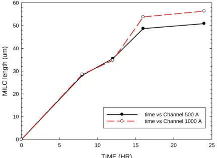
3-1.1 Effects of channel (film) thickness
MILC samples of different channel thickness, namely, 50 and 100nm, deposited on oxide substrates were characterized and compared. The MILC treatment was done at 550℃. Figure 3.1 shows experimental results on the length of MILC region as a function of treatment time for the two splits of samples. The data were obtained with optical microscopy (OM) technique. According to Wong’s report [3-1], when the channel thickness is thinner, the Ni diffusion path is more confined and more NiSi2
nodules will be trapped by the thinner geometric cross section. As a result the Ni density at the α-Si/c-Si interface is less than that of a thicker channel, thus slowing down the MILC rate. According to his data, the difference in MILC length after 24 hours anneal at 550℃ between the two splits of thickness (i.e., 50nm and 100nm) is about 5~10 um, consistent with our observation (about 6um). However, our data also indicate that the difference is negligible in the first 12 hour. If Wong’s model is correct, our observation implies that the Ni density at α-Si/c-Si interface has weak thickness dependence until 12-hour later. This also explains why the rate decreases
with decreasing channel thickness in the regime. Besides, the length saturates at around 16 hour, owing to the occurrence of SPC at the stage.
It is known that the SPC mechanism prefers to occur at the interface betweenα-Si/SiO2 layer [3-3]. In our sample, α-Si layer is pinched by two SiO2 layers
(i.e., wet Oxide and PECVD oxide). When the anneal time is sufficiently long, the nucleation of SPC poly-Si begins at or near the interface first and then grains grow, For samples with thinner channel, because of the smaller cross section area, the aforementioned process is expected to be triggered earlier which tends to deter the MILC fronts and slows down the MILC speed. In Fig. 3.1, this happens after 12hr.
3-1.2 Effects of MILC window width
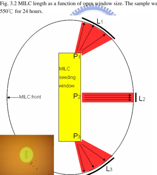
The sample characterized is with 100nm-thick channel thickness deposited on oxide-capping substrates. Seeding windows of different size (5x5, 5x10, 5x20, 5x50, 5x100 um2) were opened on the sample surface. These windows have the same slit width but different length. The sample was annealed at 550℃ for 24 hours. The results are shown in Fig. 3.2. We can see that MILC length increases with increasing window area. In addition, the dependence of MILC length on window length is not linear. Here the MILC length was measured from the central point of the slit window, as pointed out in the inset of Fig. 3.2. This result can be explained by the schematic model shown in Fig. 3.3. For a MILC pattern grown from a rectangular MILC seeding window (5μm x Xμm, X ranging from 5 to 20 μm), we can find that the MILC pattern is like an ellipse and the MILC length at the center of the long edge of the rectangle is the longest. This fact means that the MILC speed at the center of the long edge is faster, and a faster speed also suggests that the Ni concentration at this region is higher. The reason of higher Ni concentration in MILC front at this region can be explained as follows: For the Point 1(at one of the corners, denoted as P1) and Point 2
(at center of the long edge) at the seeding window edge shown in Fig. 3.3, the curvature of P1 is obviously higher than at P2. Assume that the MILC front marches radially from the seeding window, then the length of MILC front originating from P1 (L1 in Fig. 3.3) is larger than that from P2 (L2 in Fig. 3.3) due to the difference in curvature. It is thus expected that the Ni concentration at the front diminishes sooner as the curvature of the seeding window increases. As a result, the MILC speed will slow down more rapidly for the front from P1 than that from P2 due to the reduction of Ni species. For a sample with a longer MILC seeding window, the long edge center section can keep a MILC speed for a longer time due to the abundant supply of Ni species. Higher MILC speed also means that the MILC process will be less disturbed by the SPC mechanism. As a result, for a sample with a longer seeding window, the MILC front running out from the long edge center can keep higher Ni concentration and MILC speed at a farther distance from the seeding window.
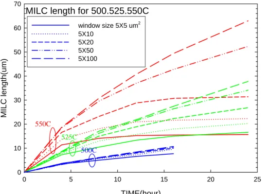
3-1.3 Temperature effects to MILC
The test samples’ thickness is 100nm. Annealing was performed at 500, 525, and
550℃, respectively, for hours. The results are shown in Fig. 3.4, in which the MILC length is shown as a function of temperature and the size of seeding window. Increase in temperature results in faster MILC speed, however, the SPC process is enhanced as well. As can be seen in the figure, the impact of temperature on MILC length becomes more profound as the window size is increased, owing to the increased supply of Ni species from the seeding window.
3-2 Characteristics of MlLC Poly-Si TFTs Fabricated with Type-A Process 3-2.1 Effects of channel length
are shown in Fig. 3.5. Figure 3.6 shows the transfer characteristics of TFTs with varied channel length from 0.6um to 10um, while the channel width is fixed at 20um. Figure 3.7 re-plots the data by multiplying the drain current (Id) with channel length for normalized comparison. Major electrical data extracted from Fig. 3.5 are shown in Table 4.1.
From Fig. 3.7, it is observed that the short channel effect is severe for the fabricated MILC devices and leads to significant Vth roll-off, especially for the device with channel length smaller than 1um. In addition, the on-state current degrades as the channel length becomes shorter. This clearly indicates that a large parasitic source/drain (S/D) resistance (Rsd) exists in our devices.
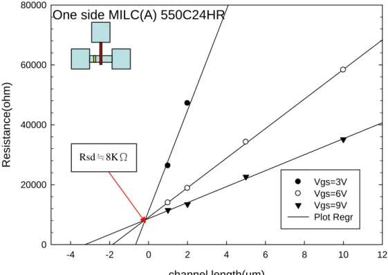
From output characteristics (Id-Vd) measurements, the Rsd can be extracted by plotting the total resistance versus channel length curves [3-6]. Figure 3.8 shows the results for the MILC (Type-A) devices. From the figure, a large parasitic resistance Rsd≒8kΩ is extracted for the devices. The resistance is much larger than that for the SPC split (i.e., α-Si film crystallized at 600℃ for 24hours before channel definition) which is smaller than 2kΩ, as shown in Fig. 3.9. Note that the two splits are actually with the same thermal budget for dopant activation (550℃ for 24hours), although the results suggest that the S/D regions of the MILC TFTs have much lower activated dopant concentration. In a previous work [3-6][3-7], phosphorus in silicon has been reported to be an effective gettering center of Ni. As a result, the active phosphorus will be reduced by Ni gettering, leading to a large parasitic resistance. Similar results have been documented previously [3-6]. This reasonably explains that the high Rsd of the MILC TFTs is caused by the insufficiently activated S/D regions.
_ ( , ) @ 0.1 , 20 Eff Vd Vd Id Vd Vg Rsd Vd V Vg V = − × = = ………...….. (3-1).
This value represents the “true” Vd value applied to the channel region accounting for the voltage drop in the S/D region. For the poly-TFTs (Type-A with one-sided MILC window), the Rsd=8 kΩ. From Table 3.1, we can see that the Eff_Vd at Vg=20V and Vd=0.1V rapidly declines when the channel length becomes shorter. As a result, the mobility calculated by Vd=0.1V condition will be underestimated.
3-2.2 Effects of MILC seeding window arrangement
From the discussion above, we know that Ni gettering is an issue for the phosphorus dopant activation. For the device with double MILC seeding windows located at the two sides of the channel, we assume that the Rsd problem will be worse than the device with single seeding window where the aforementioned Ni gettering occurs only at the source region. Figure 3.10 shows the top views of the two TFT structures with single and double MILC seeding windows. The offset from window to channel region is 5um. Figure 3.11 compares the transfer characteristics of MILC TFT (Type-A) with one- or two-sided Ni seeding window arrangement. In the figure, a larger on-current and better subthreshold swing are found for the one-sided MILC TFT. This is reasonable because for the MILC TFT with two MILC windows, the two crystallization fronts are expected to meet each other at the channel center wherein a defective region is formed. Such additional defect sites could slightly increase the subthreshold swing. The on-state current also degrades because of the larger Rsd as we just mentioned. Figure 3.12 is the plot used for extracting the Rsd of the devices with two-sided Ni seeding window arrangement. From the figure, the Rsd≒13KΩ, roughly two times larger than the devices with one-sided window.
3-2.3 Effects of channel width
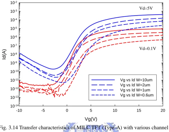
The device layout for investigating the width effect is shown in Fig. 3.13. Transfer characteristics of TFTs with various channel width but identical channel length of 2um are shown in Fig 3.14. Figure 3.15 is the normalized transfer characteristics of the same TFTs in which the Id values are normalized by the channel width. The major performance data extracted from Fig. 3.14 are shown in Table 3.2. In Fig. 3.15, the transfer characteristics with various width can be classified into two groups. The first group is the devices with channel width of 10um and 2um. In this group, the channel width is relatively wider among the test devices, and we found that the MILC region length is sufficiently long to fully crystallize the channel region of the TFTs. From the layout shown in Fig. 3.13, we can see that the width of seeding window is actually wider than the channel width. As the needle-like crystallized fronts originating from the MILC window move from the wider region to the narrower region, only the needles with direction parallel to the channel can pass and the needles with other directions will be filtered out. The film at the channel region of the device will have purer crystalline phase [3-8] [3-9]. As a result, for the device with a narrower width, better subthreshold swing (SS) and mobility performance are expected.
Nevertheless, as the device’s channel width reduces to 1um and 0.6um, referred to as the second group, an opposite trend where the mobility decreases with decreasing width is observed. This implies that the crystallization quality becomes worse with decreasing channel width. In [3-8] and [3-9], it has been shown that the MILC speed will be hindered when the MILC fronts move from a wider region into a much narrower region. This is attributed to the big mismatch between the two feature sizes, so a severe filtering effect mentioned above would retard the crystallization process. Moreover, SPC mechanism would be enhanced with a narrower channel
width due to the increasingly importance of heterogeneous nucleation events at the channel edges. For the sample with channel width of 1um, as shown in Fig. 3.14, the normalized transfer characteristics are as good as the devices of the first group at a large Vd (5V). But as the Vd is lowered to 0.1V, the subthreshold swing rises and on-current degrades. This indicates that inside the channel close to the drain region the crystallinity is worse than that near the source side (where the seeding window is located). As the width is further shrunk to 0.6 μm, the performance is further degraded, presumably due to the occurrence and dominance of SPC mechanism in the very narrow width.
3-2.4 Effects of source and drain terminal arrangement
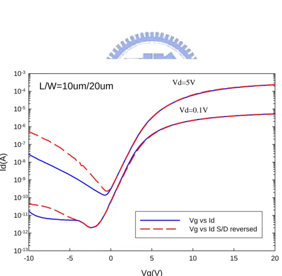
In our test structures, the MILC seeding window is nominally set at the source side with 5μm offset from the channel region. Figure 3.16 shows the comparison of transfer characteristics between the normal (also denoted as the forward mode) and the reverse mode (i.e., interchanging the source and drain bias conditions) of measurements. The L/W of devices (MILC process Type-A) are 10μm/20μm. In the figure, a larger leakage current at off-state can be found for the reverse mode. This is a clear indication that the Ni contamination is more severe in regions closer to the MILC seeding window.
3-2.5 Comparisons of one- and two-Step annealing
As introduced in Chapter 2, the devices fabricated by MILC process Type-A
have two splits for thermal anneal conditions. For most of the samples, including those discussed in previous sub-sections, MILC thermal anneal process (simultaneously with the S/D activation) was performed at 550℃ for 24hours. While for a few samples, the thermal anneal process was executed with a two-step procedure:
after the S/D implant, MILC was first performed at 400℃ for 30min, and then after removing the Ni, a 24-hour, 550℃ anneal was executed. The transfer characteristics of these devices with different anneal conditions are compared in Fig. 3.17. From the figure, the device with one-step anneal has larger on-current and better subthreshold swing than the counterpart with two-step anneal. Considering the fluctuation issue, mean value and standard deviation of leakage current (Id minima at Vd=5V), on-state Id (at Vg=20V, Vd=5V), and SS (extracted at Vd=0.1V) are compared and shown in Figs. 3.18, 3.19, and 3.20, respectively. Note that 12 samples were measured from each split. From these figures, we can see the differences between the two processes more clearly. For one-step annealed devices, more Ni species are expected to participate in the re-crystallization process and may leave more Ni residue in the channel region. And for the two-step annealed devices, the Ni diffusion from the Ni/poly-Si interface is dramatically reduced after removing the Ni source left inside the window, so the second crystallization process is mainly driven by the silicide front formed in the first step of anneal. When the MILC fronts move through the channel region, the crystallinity may be affected due to the shortage of Ni species supplied from the seeding window. As a result, the device with two-step anneal has lower on-current and worse SS.
However, the two-step annealed device has slightly lower leakage current than the one-step counterpart, owing to the reduced Ni contamination in the channel region as mentioned above.
3-2.6 Ammonia plasma treatment
For some fabricated samples, NH3 plasma treatment was performed to improve
the performance. In this section, we investigate and discuss the characteristics of these devices (fabricated with MILC process Type-A) before and after NH3 plasma
treatment. Figure 3.21(a) shows transfer characteristics before and after NH3 plasma
treatment. In the figure we can see that the MILC TFT after 1 hour plasma treatment does not show any significant improvement, while the SS is even worse than that of the fresh one. Such degradation is presumably caused by the plasma radiation. After 2 hours treatment, significant improvements in both SS and on-state current are observed, indicating that the traps inside the channel have been effectively passivated. In order to clearly identify the effect of plasma treatment on the leakage current, we extract and compare the leakage current at two bias states, namely, minima Id at Vd=5V, and Id at Vd=5V and Vg=-10V. The results are shown in Figs. 3.21 (b) and (c), respectively. The results show that, though not significant, the leakage current is improved by plasma treatment.
3-3 Characteristics of MILC Poly-Si TFTs Fabricated with Type-B Process
According to the discussion given in last section, we have learned two important facts:
1. Because the phosphorus is an effective gettering center of Ni, a high series S/D
resistance is resulted if the MILC process and phosphorus dopant activation are done simultaneously [2-1].
2. If the MILC front propagates from a wider region to a narrower region, the MILC
speed will be affected, while the film crystallinity also shows dependence on the channel width.
To address the issues encountered in process Type-A, we investigate the characteristics of MILC device fabricated with process Type-B. In this process, as introduced in Chapter 2, the MILC process was done on the blanket α-Si thin film. Because the S/D implantation and post-activation process are performed after the MILC process while the surface Ni layer has been removed, the dopant activation
process will not be seriously affected. In the following sub-sections we investigate the characteristics of the poly-Si TFT fabricated by Type-B process and check if the results can resolve the issues associated with the Type-A splits.
3-3.1 Effects of channel length
The device structure is the same as that illustrated in Fig. 3-5. Figure 3.22 shows the transfer characteristics of MILC poly-Si TFTs (Type-B) with channel length ranging from 1μm to 10μm, and identical channel width of 20μm. The MILC process was performed at 550 oC for 24 hours. Figure 3.23 re-plots the data of Fig. 3.22 normalized to the corresponding channel length. Major performance data extracted from Fig 3.22 are shown in Table 3.3. From Fig. 3.23, we can see that the on-current decreases as the channel length L is shortened. Although the trend is similar to that observed in Fig. 3-7 for Type-A devices, however, the extent of degradation is dramatically reduced. This implies that Type-B can indeed help reduce the Rsd. To confirm this inference, we extract the Rsd and the results are shown in Fig. 3.24. As can be seen in the figure, a lower Rsd 1.13KΩ was measured. This value is ≒ close to the SPC samples with the same dopant activation process (Rsd 1.1~1.6KΩ≒ , see Fig. 3.25). Figure 3.26 shows normalized transfer characteristics of the SPC samples. In this figure, minor on-current degradation for shorter channel device is also found. By comparing Fig. 3.26 with Fig. 3.23, we can conclude that the on-current degradation for shorter channel devices fabricated by either MILC process Type-B or SPC process is due to the rather high Rsd of around 1KΩ. From Fig.3.22 and Table 3.3, we can see that there is no significant difference in SS and mobility for the devices with different channel length. This indicates that Type-B devices with channel length 1~10μm have similar channel film quality. According to the analysis done in Sec.3-1, for a MILC seeding window with W/L=5μm/20μm and proceeded the
process at 550℃ for 24hours, the MILC length can reach 30μm, which is much longer than the sum of the maxima channel length(10μm) and the MIC/MILC offset(5μm)(see Fig. 3-5). The results are in agreement with the electrical characteristics of Type-B devices.
3-3.2 Effects of channel width
The device structure and layout used to investigate the effect of channel width
on the characteristics of Type-B devices are the same as that shown in Fig. 3-13. Figure 3.27(a) shows transfer characteristics of MILC TFTs with different channel width. The normalized data are shown in Fig. 3.27(b). Table 3.4 summarizes the quantified data extracted from Fig. 3.23(a). From Table 3.4, we can see that the characteristics of the devices are almost the same except for the device with the narrowest width (e.g., 0.6μm), which exhibits the best performance among the four devices in terms of SS and on-current.
The trend is significantly different from the results shown in Fig. 3.14 and Table 3-2. One possible explanation for such improvement is the presence of the parasitic conduction channels appearing at the sidewalls of the channel, as shown in Fig. 3.28. However, when we re-calculate the mobility by replacing the channel width of 0.6 μm with 0.8 μm (assuming that all of the sidewalls of the active layer serve for the channel conduction), a result of about 69.88 cm2/V*s is obtained. The value is, however, still much larger than the other samples compared in the same plot. The disparity might be related to the corners of the active layer (see Fig. 3-28). A high field-strength is expected at the corner region owing to the larger curvature. As a consequence a higher amount of inversion electrons is induced there, leading to a higher effective mobility in the simplified calculation.
Fig. 3.29 shows the normalized transfer characteristic of SPC sample and Table. 3.5 lists the major performance data. From Fig. 3.29, there is no significant difference among the devices. And from Table. 3.5, major differences come from the mobility. While the mobility increase is solely due to the increase of conduction width, since the mobility ratio coincides well with the width ratio when the sidewall conduction is taken into account. Obviously, unlike the MILC samples, the enhanced corner conduction is absent for the SPC samples. One possible explanation for this disparity is the high amount of trap states contained in the SPC channel, which may impede the modulation of surface potential.
3-3.3 Ammonia plasma treatment
Figure 3.30 shows the transfer characteristics of Type-B devices with and
without NH3 plasma treatment, and Table. 3.6 summarizes the major performance
data. In the figure we can see that the device characteristics are not improved after 1-hour treatment, and a positive shift in threshold voltage is observed. The cause for such shift is not clear at the moment, and might be related to the plasma radiation damage. After 2-hour plasma treatment, the leakage current is effectively lowered and the subthreshold swing is improved obviously. For the MILC type-A TFT, the MILC process was done after channel definition and the MILC front was confined in the channel region. More Ni contaminants are expected to be confined in the channel region and cause large leakage current. As a result, the main trap source is the metal contaminants which are not passivated by the plasma treatment. As a result the plasma treatment can not efficiently improve the leakage current. For the MILC type-B TFT, the MILC process was done on the plane α-Si layer. The MILC front is stemmed out from the seeding window and form an elliptic shape as shown in Fig. 3-2. Most of the Ni contaminants after the MILC process are expected to be located out of the channel
region and thus the concentration of the metal contaminants inside the channel is expected to be much lower than the type-A split. However, owing to the spreading out of the MILC front in the MILC type-B split, more α-Si residues between needle-like grains at the edge of the active region of the device is expected. After dopant activation at 600℃ for 24 hours, these α-Si residues become small SPC grains and contribute additional grain boundaries. As a result, the major type of defects in the MILC Type-B is that associated with the granular structure rather than the Ni contaminants. This explains why the SS is worse for the Type-B devices (Table xx). This type of defects is also known to be more efficiently improved by the plasma treatment, explaining why the leakage is lower than the Type-A split.
3-4 Leakage Mechanisms
From the quantified data of Tables 3.1~ 3.4, we can easily find that Type-A devices exhibit much better swing and slightly better mobility. However, Type-A devices also show an anomalously high off-state leakage. To understand the possible conduction mechanisms for the off-state leakage, we measure and analyze the transfer characteristics of the devices at various temperatures.
The following equation describes the relationship between temperature, activation energy and drain current [3-10]:
exp( a ) off o E I I KT = − (3-2),
where Ioff is the off-state drain current, I0 is the constant, K is the Boltzman constant,
T is the absolute temperature, and Ea is the activation energy. Take the nature logarithm of both sides of Equation 3-2, it can be expressed as follow:
ln( ) ln( ) (0 a ) off E I I KT = + − (3-3).
If we plot the Arrhenius plots of off-state drain current, the activation energy can be extracted from the slope.
Figure 3.31 shows and compares the activation energy of MILC Type-A, Type-B, and SPC samples. Figures 3.31(a) and (b) are the off-state activation energy of Type-A and Type-B devices, respectively, under forward and reverse modes of measurements at Vd = 5V. From the figures, we can see that Type-A has a high peak value of activation energy and the value is significantly affected by the gate bias. Moreover, the difference between the forward and reverse modes is significant. For Type-B, the Ea in the off-state is in the range between 0.3 and 0.6 eV and shows much weaker dependence on the bias condition, while the difference between the two modes is small. As Vgd (=Vg-Vd) increases and a strong field is developed in the channel, the tunneling distance from the valence band to conduction band is reduced, and trap-assisted tunneling may dominate for the case with sufficiently high trap state density. This will lead to a lower Ea. In our samples, such situation is more significant in Type-A devices. This is attributed to the high amount of Ni residues left in the channel after the MILC treatment. In addition, owing to asymmetrical arrangement of the seeding window in the sample characterized in Fig.3-31(a), higher amount of Ni residues is expected in the channel region near the source under the forward mode (or near the drain under the reverse mode). As a consequence the reverse mode shows a higher rate in Ea lowering than the forward mode as the Vg becomes more negative, since the high-field region is located at or near the drain junction.
Such high-field dependence of Ea is relaxed in the case of Type-B devices. As has been discussed in previous sections, although Type-B devices exhibit worse crystallinity than Type-A counterparts, much reduced amount of Ni residues is also resulted due to the unconfined MILC direction. This is also evidenced from Fig. 3-31(b) in which the difference between the two measurement modes is small. Owing
to the Ni contamination issue, a high GIDL current is observed in Type-A devices, as shown in Fig. 3-32.
In Fig. 3-31(c), the Ea of SPC sample is also shown as a reference for comparison with MILC Type-A and Type-B. From this figure, we can see that the curve for SPC sample is closer to that of Type-B device especially in the lower field region, implying the two splits have similar leakage mechanisms. Since the SPC sample does not contain Ni species, the results support the aforementioned inference. In the plot we can see that the Ea drops dramatically and begins to deviate from the result of SPC sample as Vg is smaller than -8V. This indicates that trace amount of Ni species remaining in the channel of Type-B devices may contribute to additional leakage as the field strength is sufficiently high.
3-5 Characteristics of HC-TFTs
For MILC TFTs fabricated by process Type-B, we also applied the HC-TFT structure developed by our group [1-7] to examine the device characteristics. The structure is introduced in Chapter 2. The test pattern is shown in Fig. 3.33, in which the MILC open window is designated as the source. Since the structure actually contains several transistors, for convenience, we denote the device with its S/D arrangement along the horizontal direction as the “main transistor”, and the three monitor transistors with their S/D arrangement along the vertical direction as the “DT’, “MT”, and “ST” in Fig. 3.33. Major structural parameters of several splits of devices are listed in Table 3.7. Using the HC-TFT measurement, we can study the location-dependent MILC film properties.
3-5.1 HC-TFTs for Large Scale Devices (BE1_1)
labeled as BE1_1, and the detailed structural dimensions are given in Table. 3.7. The forward- and reverse-modes Id-Vg characteristics for the main transistor of a BE1_1 device are shown in Fig. 3.34. We can see that the characteristics of the device under forward mode almost coincide with those of reverse mode.
Fig. 3.35 compares the transfer characteristics of the main transistor and the three monitor transistors and the extracted performance data are shown in Table. 3.8. The W/L ratio for the main transistor (about 0.47) and for terminal channels (about 0.42) are close so the transfer characteristics of different devices in the figure can be compared directly. From Fig. 3.35, we can see that the characteristics for the main transistor and the drain-side monitor transistor almost fall onto each other. Moreover, their characteristics are the worst in terms of the largest swing, the smallest on-current, and the highest threshold voltage, among the results shown in the figure. This implies the film quality in the main channel near the drain region is the worst. From the results presented in Sec. 3.1, the MILC length is estimated to be around 22 μm. Based on the structural parameters shown in Table. 3.7, the MILC front should stop in the channel region between the MT and the DT. This inference actually reflects on the device characteristics. As can be seen in Fig. 3.35 and the data listed in Table 3.8, the ST exhibits the best performance owing to its location being closest to the seeding window.
The off-state leakage characteristics are also investigated. Figure 3.36 shows the activation energy (Ea) of leakage current for the three monitor transistors measured at Vd=5V. In the figure, we can see that the decay rate of Ea is more significant for the ST and MT devices in the regime Vg < -10 V. From the analysis made in last section, we can consider this phenomenon an indication of higher Ni contamination. Such finding also supports the inference made in last paragraph that the MILC region actually does not cover the DT channel region. The analysis also
clearly demonstrates the effectiveness of the HC-TFT structure in resolving and identifying the film properties and the resultant electrical characteristics.
Figure 3.37 depicts the density of states (DOS) extracted from the three monitor transistors. The DOS value of the DT in the mid-gap range is larger than that of either ST or MT. This fact also agrees with the results discussed above.
Figures 3.38(a), (b), and (c) are the SEM pictures of ST, MT, and DT, respectively, taken after Secco etching [3-11]. We can see that the ST channel region is entirely MILC-dominated, but the grain direction is random. For the MT channel region, the grain size seems to be slightly larger than that in the ST channel region, and the direction of grains appears to be more uniform than ST. From the SEM image of the DT channel region, we can see the features of SPC grains [3-12]. This feature is believed to be the cause for the worse device performance of the DT.
3-5.2 HC-TFTs with Small Dimensions (BA1 and BB1 splits)
In this sub section, we present and discuss the characteristics of BA1 and BB1 HC- TFTs which have smaller dimensions than the BE1_1 split discussed above. First, let us concentrate on BA1 split, with its device dimensions detailed in Table. 3.7. Figure 3.39 shows transfer characteristics of a BA1 device (main transistor) under forward and reverse modes of measurements, and Fig. 3.40 shows transfer characteristics of the three monitor transistors inside the BA1 structure. The major difference between the forward and reverse modes of measurements is the higher GIDL leakage current under the reverse mode in off-state regime. This phenomenon is similar to that shown in Fig. 3.16, owing to the identical cause that the junction closer to the seeding window contains higher Ni contamination. From Fig. 3.40, we can see that the on-state current of three transistors are almost the same, but we can easily tell that the DT has the largest subthreshold swing and leakage current among
the three monitor transistors. This fact suggests that, the ST channel has better film quality while the film quality decays when the channel location is farther away from the MILC seeding window. This is reasonable because, for the sub channels crystallized by MILC process later, they are affected by the SPC mechanism more seriously. And as mentioned in Sec. 3.1, Ni concentration at the MILC front is gradually reduced as the front is moving out from the seeding window. Moreover, as shown in Fig. 3.41, the boundary between the MILC and SPC looks pretty rough. Some α-Si residues may be left behind at this boundary region. Such α-Si residues will become small SPC grains after the 600℃ (12 hours) dopant activation process and contribute to additional grain boundaries. Not only the on-characteristics but also the off-current will be affected if the device channel is built over this region. This is evidenced in Fig. 3-40. Figure 3.42 shows the activation energy (Ea) of drain leakage current for the three monitor transistors at Vd=5V. The difference observed in Fig. 3.36 shows up again in the figure.
Next, we discuss the BB1 devices. As shown in Table 3.7, this split has the same structural parameters as the BA1 split except with the three times larger MILC seeding window length and channel width for the main transistor (WG). Figure 3.43
shows the transfer characteristics of a BB1 device (main transistor) under forward and reverse modes of measurements, and Fig. 3.44 shows transfer characteristics of the three monitor transistors inside the BB1 structure. From the figures, we can see that the difference in the transfer curves between forward and reverse modes of the main transistor (Fig. 3.43) and among the monitor transistors (Fig. 3.44) is reduced as compared with the case of the BA1 device. In Sec.3.1, we have shown that the MILC length will be affected by the seeding window length. As a result, the MILC front is expected to pass the channels faster and farther in the BB1 device than in the BA1 device. In Fig. 3.4, for a 5μmX5μm MILC seeding window (similar to that in the
BA1 structure) annealed at 550℃, the MILC speed and length are clearly much smaller than those with a 5μmX15μm MILC seeding window (similar to those in the BB1 structure). The higher speed in the BB1 device suggests that the film properties inside the channel are much uniform as compared with that in the BA1 device. As a result, the three monitor transistors in the BB1 structure exhibit similar characteristics, although the DT still depicts a higher leakage current than the ST. Figure 3.45 shows Ea for the leakage current of the three monitor transistors. Similar trend as that shown in Fig. 3.42 is observed.
Chapter 4
Conclusions
4-1 Conclusions
In Section 3-1, the MILC length has been measured as a function of temperature, thin film thickness, and window size. These parameters are all important to the MILC process. At this section, we briefly summarize major conclusions drawn form this study:
1. The MILC process in thicker film can reach longer MILC saturation length. This is partly because the NiSi2 needles are less affected by the top and bottom
interfaces ofα-Si/SiO2, and partly because the SPC mechanism is suppressed
due to the wider spacing between the top and bottom interfaces.
2. The MILC process for a longer MILC Ni seeding window size can maintain higher MILC speed at the position farther away from the seeding window because of a higher Ni concentration maintained at the MILC front.
3. The temperature difference can effectively affect the MILC speed and MILC saturation length. At a lower temperature MILC speed is acceptable and results in a long saturation length. As the temperature is raised, although the MILC speed increases, the MILC saturation length is shortened. This is presumably due to the dramatic reduction in the incubation time of SPC mechanism and the fact that the activation energy of the MILC process is much lower than that for SPC [4-1].
In Sections 3-2, 3-3, and 3-4, two types of MILC TFTs fabricated with different MILC process flow were compared. Below are several major conclusions:
1. The TFT with MILC process Type-A has better film crystallization quality because the Ni species are mostly confined in the channel region. However, this also leads to a serious Ni contamination issue which results in a larger leakage current and can not be improved by post plasma treatment. And for the dopant activation issue, Type-A devices suffer from a large Rsd because of the Ni gettering effect.
2. Type-B devices exhibit a better off-current performance and can be farther improved by plasma treatment, owing to the less Ni residue inside the channel layer.
Finally, the MILC films were discussed by using special measurement devices. Using HC-TFT structure, the location dependence of MILC TFTs can be analyzed. We find: 1. The channels include more SPC grains when they are farther away from the
MILC Ni seeding window.
2. The on-state characteristics of MILC TFT are dominated by the portion of the channel region which has the worst film crystallinity. According to the test structure designed and fabricated in this study, such portion in the channel layer corresponds to the channel in the DT device which is the farthest away from the MILC seeding window.
References
CHAPTER 1
[1-1] G. Radnoczi, A. Robertsson, H. T. G. Hentzell, S. F. Gong, and M.-A. Hasan, ”Al induced crystallization of a-Si,” Journal of Applied Physics, Vol. 69, pp.6394, 1991
[1-2] L. Hultman, A. Robertsson, H. T. G. Hentzell, I. Engström, P. A. Psaras, ”Crystallization of amorphous silicon during thin-film gold reaction,” Journal of Applied Physics, Vol. 62, pp.3647, 1987
[1-3] S.F. Gong, H. T. G. Hentzell, A. E. Robertsson, L. Hultman, S. E. Hörnström, G. Radnoczi, ”Al-doped and Sb-doped polycrystalline silicon obtained by means of metal-induced crystallization,” Journal of Applied Physics, Vol. 62, pp.3726, 1987
[1-4] R. J. Nemanich, R. T. Fulks, B. L. Stafford, and H. A. Vander Plas, ”Initial reactions and silicide formation of titanium on silicon studied by Raman spectroscopy, ” Vac. Sci. Technol. A 3, pp.938, 1985
[1-5] Seok-Woon Lee, Yoo-Chan Jeon, and Seung-Ki Joo, ”Pd induced lateral crystallization of amorphous Si thin films,” Appl. Phys. Lett, Vol. 66, pp.1671, 1995
[1-6] Y. Kawazu, H. Kudo, S. Onari and T. Arai, ”Low-Temperature Crystallization of Hydrogenated Amorphous Silicon Induced by Nickel Silicide Formation,”
Jpn. J. Appl. Phys. Vol.29, pp.2698, 1990
[1-7] Horng-Chih Lin, Ming-Hsien Lee, and Kai-Hsiang Chang, ” Spatially Resolving the Hot Carrier Degradations of Poly-Si Thin-Film Transistors Using a Novel Test Structure,” IEEE electron device letter, Vol.27, pp.561, 2006
CHAPTER 3
[3-1] Tianfu Ma and Man Wong, ”Dopant and thickness dependence of metal induced lateral crystallization of amorphous silicon films,” Journal of Applied Physics Vol 91, pp.1236, 2002
[3-2] Y.-S. Kim , M.-S. Kim, S.-K. Joo, ”Effect of amorphous silicon shape on its metal-induced lateral crystallization rate,” Thin Solid Films, Vol 515, pp.3387, 2007
[3-3] M. Momiwa, M. Miyao, R. Tsuchiyama, M. Ichikawa, H. Sunami, T. Tokuyama, ” Preferential nucleation along SiO2 steps in amorphous Si,” Appl. Phys. Lett. Vol. 47, pp.113, 1985
[3-4] Nam-Kyu Song,z Min-Sun Kim, Shin-Hee Han, Young-Su Kim, and Seung-Ki Joo, ” Effects of Mechanical Stress on the Growth Behaviors of Metal-Induced Lateral Crystallization,” Journal of The Electrochemical Society, Vol 154, pp.370 , 2007