國 立 交 通 大 學
電信工程研究所
碩 士 論 文
兩種微小化雙模雙頻環形共振器
帶通濾波器
Two Miniaturized Dual-Mode Dual-Band
Ring Resonator Bandpass Filters
研究生:吳卓諭
指導教授:郭仁財 博士
兩種微小化雙頻雙模環形帶通濾波器
Two Miniaturized Dual-Band Dual-Mode Ring Resonator Bandpass Filter
研 究 生:吳卓諭
Student:Cho-Yu Wu
指導教授:郭仁財 博士
Advisor:Dr. Jen-Tsai Kuo
國 立 交 通 大 學
電 信 工 程 研 究 所
碩 士 論 文
A Thesis
Submitted to Institute of Communication Engineering College of Electrical and Computer Engineering
National Chiao Tung University in Partial Fulfillment of the Requirements
for the Degree of Master of science
in
Communication Engineering July 2010
Hsinchu, Taiwan, Republic of China
兩種微小化雙模雙頻環形共振器
帶通濾波器
研 究 生 : 吳 卓 諭 指 導 教 授 : 郭 仁 財 博 士
國立交通大學電信工程研究所
摘要
本論文提出兩種微小化雙模雙頻環型共振器濾波器的設計。第一
種設計使用單一週期性步階阻抗環型共振器實現雙模雙頻濾波器。利
用傳輸線理論,將輸出輸入端埠以不同的饋入角度畫出對應的傳輸零
點與共振極點位置,稱之為傳輸零點圖。實際設計電路時,可以根據
本圖很容易選擇饋入角度,得到通帶兩側均具有傳輸零點之準橢圓函
數的雙模雙頻響應。這一部分,本文有四個實作雙模雙頻濾波器,電
路的面積僅佔傳統環型電路的 60%。
論文的第二部分利用串接許多微波 C 型段組成微小化雙模雙頻環
型濾波器,每一微波 C 段均可等效為一段電氣長度給定的傳輸線,
再經由選擇適當的饋入角度,則也可以達到準橢圓函數響應。本文分
別使用四段 C 型段與六段 C 型段實做出環型共振器濾波器,其面積
Two Miniaturized Dual-Mode Dual-Band Ring
Resonator Bandpass Filters
Student: Cho-Yu Wu
Advisor: Dr. Jen-Tsai Kuo
Institute of Communication Engineering
National Chiao Tung University
Hsinchu, Taiwan
Abstract
The thesis presents two designs of miniaturized dual-mode dual-band ring resonator bandpass filter. The first design uses a single periodic stepped-impedance ring resonator. Based on the transmission line theory, a pole-zero design graph consisting of the transmission zeros together with the resonant frequencies of the resonator is plotted against the space separation angle between the input and output ports. Based on this graph, the space angle can be determined for the dual-mode dual-band design with designated zeros near the two passbands. Four dual-mode dual-band bandpass filters are realized for demonstration. All circuits occupy about 60% of the area of the conventional ring resonator at the first passband frequency.
In the second part of this thesis, the ring resonator is implemented by a cascade of several microwave C-sections. Each C-section is used to substitute a transmission line section of designated electrical length. Through proper design of input/output coupling configuration, two transmission zeros can also be created on both sides of each passband. Two circuits with four and six microwave C-sections are fabricated for demonstration. They occupy less than 30% of the area of a traditional ring resonator filter. Measured results agree very well with their simulation counterparts.
Acknowledgement
致 謝
能順利完成這篇論文首先要感謝的是我的指導老師,郭仁財教
授。在郭老師這二年來的耐心和辛苦的指導下,讓我對微波領域有更
進一步的了解。老師的嚴謹思維與處事態度無時不刻提醒著我要以老
師為楷模。也很謝謝口試委員:鐘世忠教授、張盛富教授和金國生教
授,對學生的論文提出指教和提供寶貴的意見。
感謝郭建男教授一年多來的指導,讓我對微波實務和主動電路部
分有初步的了解。也感謝高雄大學吳松茂教授,在帶我進入微波領域
的同時也給我很大的鼓勵讓我能順利的考上交通大學研究所。
很感謝逸群學長,對我的研究幫助甚多。感謝已畢業秉岳、政良、
評翔、正修、裕豪學長。感謝在同一實驗室奮鬥的同伴:麒宏、峻瑜、
紹展、宣融、詩薇、祖偉,和學弟們:孟修、佑先,還有我找工作時
幫我很多的志銘學長,修課時幫了很多忙的玄德學長,謝謝你們。
在新竹這幾年,要特別謝謝舅舅和舅媽的照顧,讓我常常有免費
的大餐可以吃。謝謝千蕙兩年多來的陪伴,共度許多困難的關卡。最
後要感謝我的父母親在我最難過的時侯給予我最大的支持和鼓勵,讓
我能全心全力的投入學業上,您們是我最重要的依靠也是我做事情的
榜樣。
Contents
Chinese Abstract
... iEnglish Abstract
... iiAcknowledgement
... ivContents
... vList of Figures
... viChapter 1
Introduction ... 1Chapter 2
Dual-Mode Dual-Band Filter With Periodic Stepped-Impedance Ring Resonator (PSIRR) ... 42.1 Uniform Ring Resonator (UIR) ... 5
2.2 Transmission Zeros of Uniform Ring Resonator Filter ... 6
2.3 Periodic Stepped-Impedance Ring Resonator (PSIRR) ... 8
2.4 Transmission Zero Design Graph ... 10
2.5 Simulation and Measurement ... 13
Chapter 3
New Miniaturized Dual-Mode Dual-Band Ring Resonator Bandpass Filter With Microwave C-Sections ... 32
3.1 Analysis of the Microwave C-Section ... 33
3.2 Transmission Zeros and Bandwidth Control With Perturbation Patch ... 35
3.3 Simulation and Measurement ... 36
Chapter 4
Conclusion ... 45List of Figures
Figure 2-1 The uniform impedance microstrip ring resonator with feed line ... 18 Figure 2-2 Simulated resonant characteristic of a UIR in Figure 2-1 for n = 1 to 5. ... 18 Figure 2-3 Simulated response of the UIR with ro = 12.3 mm, ri = 11.7 mm and patch
area = 2×3 mm2 when the space between input and output ports is 90°. ... 19 Figure 2-4 Uniform impedance resonator using even- and odd-analysis. ... 19 Figure 2-5 Transmission zero design graph for the UIR with ZR = 70 ZP = 40 and
P = 10o. ... 20
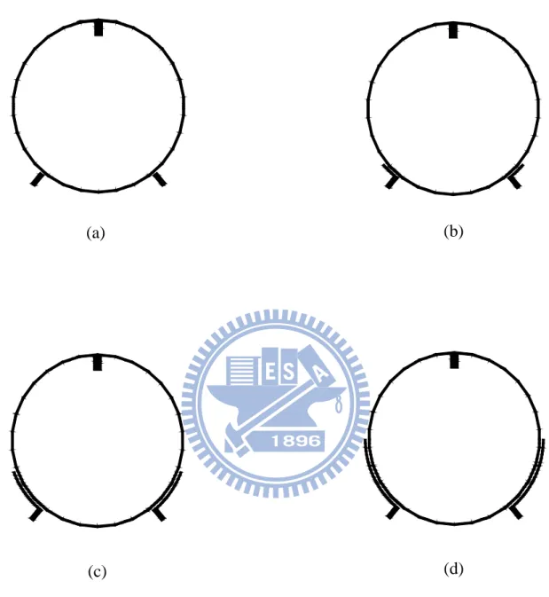
Figure 2-6 Four excitation schemes with improving insertion loss... ... 20 Figure 2-7 Four UIR circuits with line-to-ring coupling of different coupled line
lengths. (a) length = 0o. (b) length = 10o. (c) length = 30o. (d) length = 50o. All electrical lengths are at the first resonant frequency. ... 21 Figure 2-8 Simulation results of four UIR circuits with different coupled-line lengths.
... 22 Figure 2-9 The periodic stepped-impedance ring resonator with line-to-ring coupling
structures. (a) N = 8. (b) N = 6. ... 22 Figure 2-10 The periodic stepped-impedance ring resonator with N = 6 in the even-
and odd-analysis. ... 23 Figure 2-11 Resonant spectrum of the PSIRR. R = 3 and R’ = 3.6 for N = 6 and 4. R =
1 = 2/N – 2. ... 23
Figure 2-12 fna, fnb, f2/f1 and f3/f1 versus R. N = 8, R’ = 0.5R. ... 24
Figure 2-13 Transmission zero design graph for the PSIRR with N = 8. R = 3, R’ = 0.5R. ... 24
Figure 2-14 Test of |S21| responses for the ring resonator filter with N = 8. (a) f1. (b) |S21| at f2. Z1 = 80 , Z2 = 25.3 , Z3 = 55.8 . ... 25
Figure 2-15 Transmission zero design graph for the PSIRR with N = 6. R = 3, R’ = 3.6. ... 25
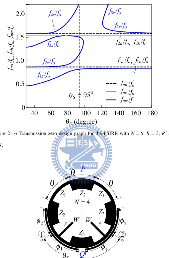
Figure 2-16 Transmission zero design graph for the PSIRR with N = 5. R = 3, R’= 0.5R. ... 26
Figure 2-17 The N = 4 periodic stepped-impedance ring resonator with line-to-ring coupling structure and two open stubs. ... 26
Figure 2-18 Variations of fna, fnb and fmz with respect to the open stub length. W = 0.2 mm, Z1 = 91.3 , Z2 = 30.4 , Z3 = 25 . ... 27
Figure 2-19 Design procedure for N = 5, 6, and 8...27
Figure 2-20 Simulation and measured of PSIRR with N = 8. ... 28
Figure 2-21 Photograph of PSIRR with N = 8 for the results in Figure 2-20. ... 28
Figure 2-22 Simulated and measured results of the bandpass filter with N = 6. Circuit parameters: Z1 = 91.3 , Z2 = 30.4 , Z3 = 27.3 , Zp = 0.26 mm2, = 27o, and = 63o. ... 29
2-22. ... 29
Figure 2-24 Performances of dual-mode dual-band bandpass filter with N = 5. Circuit parameters: Z1 = 90.5 , Z2 = 30.2 , Z3 = 77.1 , Zp =0.38 0.27 mm2, 1 = 40o, and 2 = 0o. ... 30
Figure 2-25 The dual-mode dual-band bandpass filter with N = 5 for the result in Figure 2-24. ... 30
Figure 2-26 Performances of dual-mode dual-band bandpass filter with N = 4. Circuit parameters: Z1 = 91.3 , Z2 = 30.4 , Z3 = 25 , = 3.6 mm, 1 = 40o, and 2 = 40o. ... 31
Figure 2-27 Photograph of PSIRR with N = 4. ... 31
Figure 3-1 Microwave C-section. ... 39
Figure 3-2 Phase response of the microwave C-section with different Zoe/Zoo. ... 39
Figure 3-3 The proposed elementary two-port for substituting a transmission line section. ... 40
Figure 3-4 Zoe, Zoo and c as functions of n. ... 40
Figure 3-5 Dual-mode dual-band ring resonator bandpass filter with four C-sections. ... 41
Figure 3-6 Dual-mode dual-band ring resonator bandpass filter with six C-sections. 41 Figure 3-7 |S21| response of Figure 3-5 with c1 = c2 = 0. ... 42
Figure 3-8 Simulated and measured results of the ring filter with four microwave C-sections. ... 42
Figure 3-9 Photograph of the experimental circuit with four microwave C-sections. . 43 Figure 3-10 Simulated and measured results of the second dual-mode dual-band ring
filter with six microwave C-sections. ... 43 Figure 3-11 Photograph of the second dual-band filter with six microwave C-sections.
Chapter 1
Introduction
The microstrip ring resonator has been widely used to evaluate phase velocity, dispersion characteristics, and effective dielectric constant of microstrip lines. Many applications, such as bandpass filters, oscillators, mixers, and antennas using ring resonators have been reported [1]. The ring resonator bandpass filter has many attractive features such as low cost, compact size, high selectivity, and a simple design procedure. There have been a series of innovative analysis, design and realization of the ring resonator filters [2]-[7]. These bandpass filters built by dual-mode ring resonators could be originally presented by Wolff [2], where two degenerate modes of the ring are excited by asymmetrically coupling and disturbed by a notch. In [3], a joint field/circuit model is proposed to characterize the line-to-ring coupling structures for design and optimization of microstrip ring resonator circuits. With suitable perturbation and input/output design, a quasi-elliptic bandpass filter is designed to have tunable transmission zeros and keep the bandwidth constant at the same time [4]. In [5], based on transmission-line theory, the resonance frequencies of ring resonator with a perturbation are analyzed. In [6], the periodic stepped-impedance ring resonator is devised to design dual-mode bandpass filters with a miniaturized area and wide upper stopband. In [7], the ring resonator using broadside-coupled section only occupies 19.3% of the area of conventional ring resonator. Notice that all
aforementioned dual-mode ring filters involve only a single passband.
Recently, rapid development of modern wireless systems, such as GSM and WLAN, has created a need for dual-band RF devices. So, several dual-mode dual-band bandpass filters have been published [8]-[11]. In [8], a stacked-loop structure is used to design dual-mode bandpass filters with a dual-band response. The circuit consists of two dual-mode loop resonators, and each resonator controls one passband. This idea is extended to an alternative dual-band filter excited with CPW feed lines [9]. In [10], a loop resonator is proposed for a planar dual-band filter. The feed lines are placed between two resonators to offer sufficient coupling for both passbands. The dual-band filter in [11] is designed in a multilayer structure consisting of dual-mode resonators in a reflector cavity. It is noted that each selected passband in [4]-[11] is mainly controlled by a resonator.
So far, it is still challenging to design dual-mode dual-band circuits with a single resonating element. The circuit area, and hence the cost, can be reduced to half, if a single resonator is used. In [12], the circuit resonator is a cross-slotted patch combined with a square aperture. The dimensions of the slots and the aperture determine the two frequencies. In [13], the filter has a tunable second passband. In [14], non-degenerate dual-mode slow-wave open-loop resonators are used. It is interesting to note that the two modes are uncoupled. In [15], the inner peripheral of
In this thesis, we propose two novel miniaturized dual-mode dual-band ring resonator bandpass filters. In Chapter 2, we extend the use of the periodic stepped- impedance resonator in [6] to development of dual-mode dual-band filters. While the resonator in [6] is designed for a single passband, the resonator here is treated as a dual-frequency element and perturbations are used to control the two resonances at each designated frequency. A new pole-zero design graph is devised to facilitate the circuit realization. The zero frequencies and the space angle of the input/output ports can be easily determined by the graph. Four dual-mode dual-band filters are fabricated and measured for validation.
In Chapter 3, we propose a new idea of designing dual-mode dual-band bandpass filter implemented with the microwave-C sections, which have a nonlinear phase shift property in frequency [16] and are suitable for developing dual-band devices [17]. Here, each microwave C-section is used to substitute a /4- or /6-section of a traditional ring. Analysis will be conducted and design curves plotted for facilitating the circuit realization. Emphasis is also put on the input/output configuration for creating transmission zeros on both sides of each passband. The ring resonator with microwave C-section occupies less than 30% of the area of conventional ring resonator
Chapter 2
Dual-Mode Dual-Band Filter With Periodic
Stepped-Impedance Ring Resonator (PSIRR)
In this Chapter, we start with a brief analysis of uniform-impedance ring resonator. The analysis includes the basic resonance condition of a ring resonator and transmission zeros with different spatial angles between the input and output ports. Then, we extend the uniform-impedance ring resonator to the periodic stepped-impedance resonator. We devise the pole-zero design graph consisting of transmission zeros together with the resonant frequencies of the resonator against the space separation angle between the input and output ports. As a result, dual-mode dual-band filter with designated zeros near the two passbands can be achieved. The bandpass filter has not only good frequency selectivity but also an area of about 60% of that of a conventional dual-mode ring resonator filter.
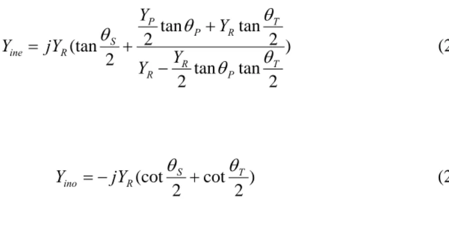
2.1 Uniform Ring Resonator (UIR)
The ring resonator is merely a closed circular loop formed by a transmission line. A ring resonator filter consists of feed lines, coupling gaps and the ring, as shown in Figure 2-1. The signal power is coupled into and out of the resonator through the feed lines and coupling gaps. The effect of the coupling gaps on the resonant frequencies of ring can be neglected for a large distance between the feed lines and the resonator. This loose coupling can be equivalent to a negligibly small capacitor between feed lines and resonator. If the feed lines are moved closer to the resonator, however, the coupling becomes tight and the gap capacitances become appreciable. This will cause the resonant frequencies of the circuit to deviate from the intrinsic resonant frequencies of the ring. It is worth mentioning that the tight coupling structure can be exploited to reduce insertion loss in the passband for the design of the bandpass filter.
When the mean circumference of the ring resonator is equal to an integer multiple of a guided wavelength, resonances occur. At resonances, we have
2 π r = n λg for n = 1, 2, 3, … (2.1)
where r is the mean radius that equals the average of the outer and inner radii of the ring, λg is the guided wavelength, and n is the mode number. This relation is valid for
loose coupling case, as the coupling gap effect is not included. For the first mode, the maximum of field occurs at the input and output positions and the nulls occur at 90° from the coupling gap locations. For a microstrip ring, λg can be expressed as
f c eff eff g 1 (2.2)
where c is the speed of light and is the effective dielectric constant of the eff microstrip. From (2.1), the resonant frequencies can be written as
eff r nc f 2 for n = 1, 2, 3, … (2.3)
Figure 2-2 shows the simulated resonant frequencies of some leading modes of an uniform ring resonator using loose coupling with outer radius ro = 12.3 mm and inner
radius ri = 11.7 mm on a substrate with relative dielectric constant r = 10.2. The
electromagnetic simulator IE3D [18] is used for simulation.
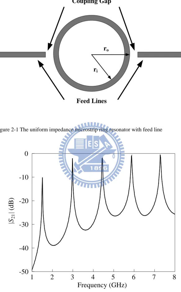
2.2 Transmission Zeros of Uniform Ring Resonator Filter
Figure 2-3 shows the response of a traditional dual-mode ring resonator filter with a perturbation patch (Zp) when the space between input and output ports is 90°
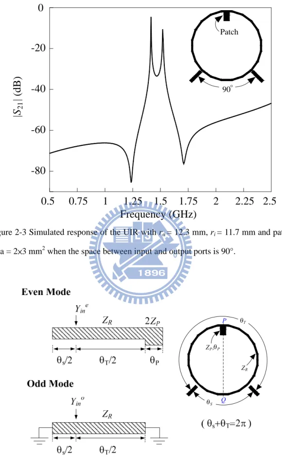
[5]. These zeros are attractive for filter design since they improve the frequency selectivity. The transmission line theory can be used to calculate these zeros. By attaching the input and output ports directly to the ring and applying the even- and odd-mode analysis to the symmetrical circuit as shown in Figure 2-4, the input admittances Yine (PQ plane open-circuit) and Yino (PQ plane short-circuited) can be
) 2 tan tan 2 2 tan tan 2 2 (tan T P R R T R P P S R ine Y Y Y Y jY Y (2.4) ) 2 cot 2 (cot S T R ino jY Y (2.5)
The transmission zeros can be obtained by solving Yine = Yino. Apparently, the roots of
Yine - Yino = 0 will be functions of s, i.e. the spatial angle between the input and output
ports.
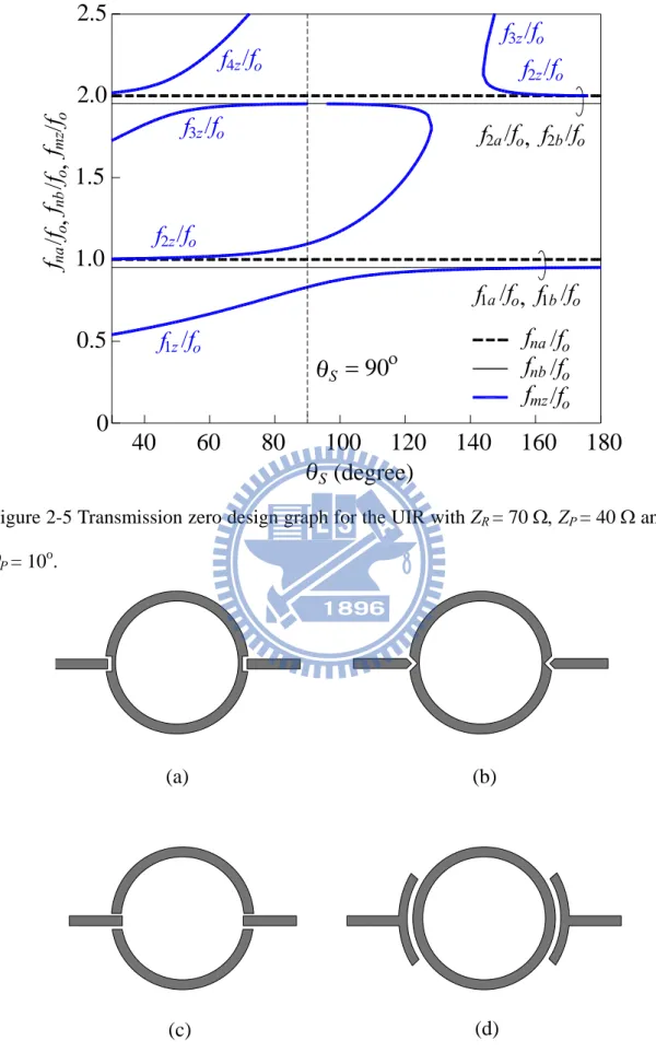
Figure 2-5 shows fna, fnb and the transmission zeros fmz as functions of s for
uniform ring resonator, where n and m are positive integers. All these data can be calculated by a root-searching program. Obviously, all fna and fnb will be independent
of s, since they are natural frequencies of the resonator and will not be affected by
any s. For the transmission zeros, they can be adequately adjusted by tuning the s. It
is interesting to note that when s = 90°, the first passband will be symmetric about f1
since f1z and f2z are symmetrically allocated on both sides of the passband, but the
second passband will have only one resonance because f3z eliminates the f2b.
To improve high insertion loss caused by loose couplings, many new configurations have been investigated [19]-[23]. The enhanced coupling configurations with minimum perturbation shown in Figure 2-6a, b and c are designed to improve the insertion loss. For filter applications, the line-to-ring structure is usually used to obtain a better insertion loss. A ring resonator with more coupling
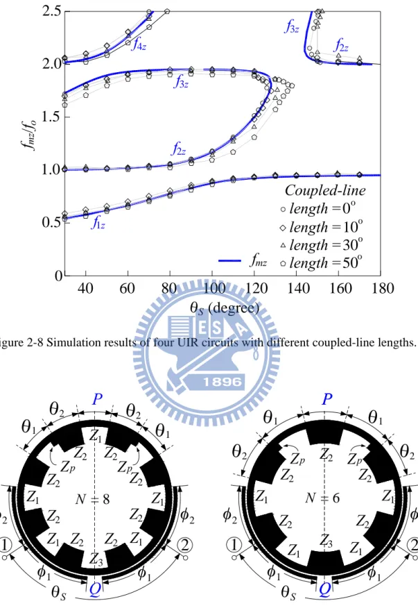
periphery is shown in Figure 2-6d. If the line-to-ring structure is used, the insertion losses will be better but the resonance frequencies will also be affected.It is intuitive that the longer the line-to-ring structure, the greater the effect on the resonance frequencies and transmission zeros. To investigate the effect of the line-to-ring structure on the transmission zeros of the ring resonator filter, four ring circuits designed at a fundamental frequency of 1 GHz with different coupled line length are simulated using IE3D [18]. The layouts of the four circuits are in Figure 2-7, and responses are shown in Figure 2-8. For the sake of simplicity, resonant frequencies are not plotted here. As shown in Figure 2-8, the transmission zeros of the filter with the longest coupled line have the lowest frequencies. When coupled-line length > 50° the |S21| deceased and the |S11| increased because the circuit is over-coupled. We conclude
that due to the line-to-ring structure when coupled-line length ≦ 50°, the resonant frequencies and the transmission zeros shift to lower frequencies when the length of the coupled-line is increased.
2.3 Periodic Stepped-Impedance Ring Resonator (PSIRR)
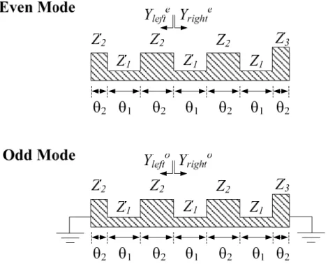
As described in [6], the ring peripheral of a periodic stepped-impedance ring resonator (PSIRR) consists of interlaced hi-Z and low-Z sections. Let N denote the number of periods in the ring. Figure 2-9 shows two such rings with N = 8 and 6 of
The perturbation Z3 in the plane of symmetry PQ is used to split off the
degenerate modes. Two additional patches denoted by Zp are also incorporated for
perturbation. However, they are not used in analysis until the circuits are realized in Section 2.5. The resonant condition for PSIRR can be derived by the transmission-line theory [5]. For example, the PSIRR with N = 6 can be modeled by the multistepped-impedance lines as shown in Figure 2-10. Its odd and even resonance frequencies can be obtained when the PQ plane is treated as short- and open-circuited, respectively. For the even mode,
righte
0
e leftt evenY
Y
Y
(2.6) ) 2 cot tan ( tan ) tan 2 cot ( ) tan 2 cot ( tan ) 2 cot tan ( 1 2 2 1 1 1 1 1 2 2 1 2 1 2 2 1 1 2 2 2 1 1 1 2 Z Z Z Z Z Z Z Z Z Z Z Z jZ Y e left (2.7) 1 1 1 1 1 tan tan 1 jZ Z jZ Z Z Yrighte (2.8) ) 2 cot tan ( tan ) tan 2 cot ( ) tan 2 cot ( tan ) 2 cot tan ( 2 3 1 1 1 1 1 2 3 1 2 1 2 3 1 1 2 2 3 1 1 1 2 Z Z Z Z Z Z Z Z Z Z Z Z jZ Z (2.9)readily obtained. Figure 2-11 plots the split up modal frequencies fna and fnb (n = 1 ~ 3)
against 2 for the resonators with R = Z1/Z2 = 3 and R’ = Z1/Z3 = 1.2R for N = 4 and 6,
and R = 3 and R’ = 0.5R for N = 5 and 8. Note that fna and fnb are calculated by
treating the PQ plane as an electric and magnetic wall, respectively. All frequencies are normalized with respect to the fundamental frequency of a uniform ring resonator,
fo. It is noted that the impedance junctions between the low- and high-impedance
sections are not taken into account for the sake of simplicity.
Figure 2-12 investigates the changes of fna and fnb and of ratios f2/f1 and f3/f1 with
respect to variation of R for resonator with N = 8. The purpose of the ratio f3/f1 is to
check the unwanted resonance next to the second passband. One can see that all resonances shift down to lower frequencies as R is increased. The ratio f2/f1 moves
from 2.0 to 1.89 when R is increased from 1 to 8.
2.4 Transmission Zero Design Graph
In [5], the resonance frequencies and transmission zeros of a dual-mode ring resonator bandpass filter are calculated by the transmission line theory. Thus, the transmission zero design graph can be plotted against the space separation angle between the input and output ports. The transmission zeros of the periodic stepped-impedance resonator can be calculated as follows. Let the lengths of upper
circuited) and Yino (PQ plane short-circuited). Then, we can solve the nonlinear
equation 0YineYino to calculate the zeros. Figure 2-13 shows the transmission zeros for a PSIRR with N =8. Apparently, the transmission zeros are functions of S. It
can be observed that there are two zeros on both sides of the two split-up degenerate modes. For the first passband, it suggests S be between 65o and 115o, since the
passband may be altered when fmz is too close to fna or fnb. When S < 60o and S >
120o, f1z and f2z are close to f1b and f1a, respectively. Also, f3z and f4z have a close
proximity to f2b and f2a as 55o < S < 125o and S < 40o or S > 140o. When S = 180o,
f1z and f4z are in near neighborhoods of f1b and f2a, respectively. It is worth mentioning
that passband response can be greatly affected if any zero gets too close to the resonant peaks. It is interesting to note that f2z and f3z merge together at certain S
point, and so f4z and f5z do.
Figure 2-14 plots the simulated |S21| responses in the first and the second bands
using the software package IE3D [18], for a PSIRR filter with N = 8, Z1 = 80 , Z2 =
25.3 and Z3 = 55.8 and 1 = 2 = 0 for S = 90o, 112.5o and 135o. The substrate
has r = 10.2 and thickness = 1.27 mm. The feed lines are separated from the ring by a
small gap. When S = 90o, the two peaks in the first band have a similar |S21| level. It
will lead to a symmetric passband. In the second band, however, only one peak exists since f2b is suppressed by f3z, as validated by Figure 2-13. When the separation angle
S = 135o, the two peaks in the second band have a similar |S21| level, but there is no
the two peaks in both bands are less than 7 dB. Note that in this case each lower peak is neighboring with a transmission zero. Thus, both passbands may have an asymmetric response when the two peaks have identical input and output coupling [6].
Figure 2-15 and Figure 2-16 show the resonances fna and fnb and zeros fmz against
S for the resonator with N = 6 and N = 5. Note that f3a is not shown since it is far
away from f3b for N = 6 (See also Figure 2-11).
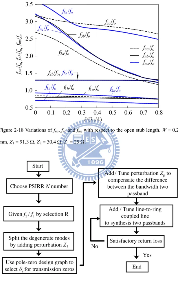
Figure 2-11 shows the second resonances of PSIRR with N = 4 are not degenerate, and f2a is far away from f2b. This introduces a challenge to synthesis of the
second passband. To tackle this problem, extra open stubs (width W and length ) are incorporated into the design. Figure 2-17 draws the circuit layout, showing that the stubs are attached to the middle of the Z1-section and have a space angle of 45o away
from the plane PQ. Consider the lower-right quarter of the ring. The resonances f2a
and f2b are the natural frequencies of a stepped-impedance (Z2-Z1-Z2) section when the
centers of the Z2 sections are short-circuited and open circuit, respectively. Thus, the
center of Z1 is a virtual ground point at f2b, and an open circuit point at f2a. Attaching
any stub to this point will not alter f2b but will bring f2a down to lower frequencies,
depending on the lengths of the stubs [24]-[25]. Here, two stubs, rather than four for all the centers of the Z1-sections, are sufficient for the frequency tuning purpose.
resonator with line impedance Z1 at f1. Here, the S = 90o is used. It is worth
mentioning that these results are obtained by direct computation based on the transmission-line theory, as those in Figures 2-12, 13, 15 and 16. One can see that f2a
and f3b shift down rapidly to lower frequencies as /(1/4) is increased. This is because
at the f2a and f3b resonances the open stubs are attached to the positions where
maximal voltages occur. Note that f2b does not change when /(1/4) is changed, and
that f2b is collocated with f3z since S = 90o is used. It is worth mentioning that the two
resonances and the two zeros of the first passband decrease slowly and simultaneously when is increased, and that f4z > f3b when /(1/4) < 0.08 or /(1/4) > 0.375. The
/(1/4) here is selected as 0.4 to synthesis the dual-mode dual-band bandpass filter.
2.5 Simulation and Measurement
Four dual-mode dual-band PSIRR bandpass filters are fabricated on a substrate with r = 10.2 and thickness = 1.27 mm. The design procedure for N = 5, 6, and 8 is
shown in Figure 2-19.
Figure 2-20 plots the simulated and measured results of the N = 8 dual-mode dual-band filter with S = 112.5o. It is designed to have f1 = 2.5 GHz and f2 = 4.72
GHz and fractional bandwidths 1 = 6.04% and 2 = 5.51%. The circuit parameters
are the same as those used in Figure 2-14. The corresponding line widths for the sections Z1, Z2 and Z3, are 0.36, 3.80 and 0.93 mm, respectively. The outer radius of
conventional dual-mode ring filter operating at f1. The gap size between the
line-to-ring coupler and the ring resonator is 0.15 mm, and 1 = 51o and 2 = 39o. The
line-to-ring coupler has to support the two passbands simultaneously.
The patches Zp are used to trim the bandwidths. As shown in Figure 2-14, the
distance between the two peaks at f2 is larger than that at f1, so it needs more coupling.
In this case, however, stronger coupling with larger 1 and 2 will cause the response
at f1 to be over-coupled. Thus, the patches are added at virtual short-circuited
positions for the even mode resonance at f2, leading to a shorter distance between the
two peaks so that the required coupling level needs no more increment. At the same time these positions are the open circuit points for the resonances at f1. The patches
bring both resonances at f1 to shift down together, but the change of bandwidth is
negligible. The size of Zp is 0.50.37 mm2.
In Figure 2-20, the measured insertion losses are 1.9 dB and 1.5 dB and return losses are better than 18 dB and 15 dB at f1 and f2, respectively. The four transmission
zeros are at 2.42 GHz, 3.5 GHz, 4.55 GHz and 5.85 GHz, offering good transition responses. The first spurious in the upper rejection band occurs at 6.3 GHz, which is close to the theoretical value (point A) in Figure 2-12. Figure 2-21 shows the photograph of the experimental circuit.
resonant frequency f3a is much larger than f3b, a wider upper stopband can be achieved
if the resonance at f3b can be suppressed. This can be done by allocating the zero f5z
very close to it, leading to the separation between the input and output S = 62.5o, as
shown by the dashed line in Figure 2-15.
For the resonant spectrum of N = 5 as shown in Figure 2-11, the resonant frequencies f3a and f3b are higher than f2a and f2b, and a desirable upper stopband can
be realized easily. Here, we have a degree of freedom to select S for the transmission
zeros, so that a wide stopband can also be achieved at the same time.
Figure 2-22 presents the simulated and measured results of the PSIRR bandpass filter with N = 6. Both the line width and gap size of line-to-ring structure are 0.2 mm. The radius of the ring is 5.67 mm, and its normalized area is 57.2%. The circuit has f1
= 2.49 GHz and f2 = 4.77 GHz with fractional bandwidths 1 = 8.11% and 2 = 4.54%.
The measured |S21| at f1 and f2 are 2.39 dB and 2.2 dB, respectively, and |S11| at both
frequencies are better than 15 dB. The two pairs of zeros located at both sides of passbands are 1.93 GHz, 2.57 GHz, 4.35 GHz and 5.49 GHz. Since f3b is totally
suppressed by f5z, the circuit demonstrates an improved upper stopband performance
as compared with the previous filter with N = 8. Again, two Zp patches are
incorporated into the circuit for tuning the passbands. The measured data show reasonably good agreement with the simulation. Figure 2-23 shows the photograph of the measured circuit.
with N = 5. The circuit has f1 = 2.48 GHz and f2 = 4.55 GHz with fractional
bandwidths 1 = 4.03% and 2 = 3.77%. Figure 2-25 is the photo of PSIRR bandpass
filter with N = 5. The radius of the resonator is 6.04 mm, and it occupies about 65% of the area of a conventional ring resonator at the first frequency. The circuit also demonstrates an improved upper stopband performance. In the case, we have the freedom in choosing the position of transmission zeros as compared with the PSIRR filter with N = 6. The four transmission zeros located at both sides of passbands are 2.37 GHz, 3.27 GHz, 4.42 GHz and 6.71 GHz. The measured result has good agreement with the simulation.
Figure 2-26 plots the simulated and measured results of the filter with N = 4. The value of /(1/4) is selected as 0.4. Note that f1a and f1b support the first passband and
f2a and f3b establish the second one. The latter two resonances are non-degenerate
modes, like the design in [14]. The circuit has f1 = 2.47 GHz and f2 = (f2a + f3b)/2 =
5.83 GHz with 1 = 5.39% and 2 = 7.07%, respectively. Note that the ratio f2/f1 =
2.36 > 2. The measured |S11| and |S21| are –10.2 dB and –1.6 dB at f1 and –31.1 dB
and –2.18 dB at f2. The |S21| glitch around 4 GHz confirms the fact that f2b is
suppressed by f3z. The peak at 6.75 GHz is f3a, which is 2.8 f1 and has about 7% error
compared with the curve shown in Figure 2-17. The deviation could be due to the parasitic effects of the impedance junctions which are not taken into the account in the
Coupling Gap
Feed Lines
r
ir
oFigure 2-1 The uniform impedance microstrip ring resonator with feed line
Frequency (GHz)
1
2
3
4
5
6
7
8
21|
S | (dB
)
-50
-40
-30
-20
-10
0
Frequency (GHz)
21|
S | (dB)
-20
0
0.5
0.75
1
1.25
1.5
1.75
2
2.25 2.5
-40
-60
-80
Patch 90oFigure 2-3 Simulated response of the UIR with ro = 12.3 mm, ri = 11.7 mm and patch
area = 2×3 mm2 when the space between input and output ports is 90°.
P Q S T P Z ,P R Z
S(degree)
0
0.5
1.0
1.5
2.0
2.5
180
S90
f
mz o/f
/f
o nbf
,
,
f
na o/f
o/f
o/f
/f
o mzf
f
nb naf
f
1b/f
o o/f ,
1af
f
1z/f
o o/f
2zf
o/f
3zf
o/f
4zf
f
2z/f
of
3z/f
of
2b/f
o o/f ,
2af
40
60
80
100
120
140
160
Figure 2-5 Transmission zero design graph for the UIR with ZR = 70 ZP = 40 and
P = 10o.
(a) (b)
(c)
(a) (b)
(d)
Figure 2-7 Four UIR circuits with line-to-ring coupling of different coupled line lengths. (a) length = 0o. (b) length = 10o. (c) length = 30o. (d) length = 50o. All electrical lengths are at the first resonant frequency.
f
mz o/f
f
3zlength =30
length =50
length =0
Coupled-line
o o o of
mz
S(degree)
0
0.5
1.0
1.5
2.0
2.5
180
3zf
length =10
40
60
80
100
120
140
160
f
4zf
2zf
2z 1zf
Figure 2-8 Simulation results of four UIR circuits with different coupled-line lengths.
pZ
1Z
1Z
pZ
2Z
Z
2N = 8
Z
2Z
2
1 2
Z
3
1
1
2 SQ
12
2
1
P
2Z
pZ
pQ
P
2Z
2Z
P
Q
1Z
Z
3
S2
1
2 1
2
1
1
2 2 1Z
1Z
1Z
2 1Z
1Z
Z
2N = 6
Z
2
Z
1Z
1Z
2 2Z
2Z
2Z
Figure 2-10 The periodic stepped-impedance ring resonator with N = 6 in the even- and odd-analysis. 2
90
80
70
60
50
Resonant frequencies
o/f
,
naf
o/f
nbf
(degree)
N = 8
N = 4
N = 4
4.0
3.5
3.0
2.5
2.0
1.5
1.0
0
10
20
30
40
0.5
N = 4
N = 5
N = 4
0.5
40
30
20
10
f
0
1.0
1.5
2.0
2.5
3.0
3.5
4.0
na nbf
N = 4
N = 4
(degree)
f
nb/f
of
na,
/f
oResonant frequencies
/f
o o/f
N = 6
50
60
70
80
90
2 Figure 2-11 Resonant spectrum of the PSIRR. R = 3 and R’ = 3.6 for N = 6 and 4. R = 3 and R’ = 1.5 for N = 8. fo is the fundamental frequency of a uniform ring. 1 =
R
1
0.5
1.0
1.5
2.0
2.5
3.0
2
3
4
5
6
7
8
f
nb naf
1.5
2.0
2.5
3.0
1.75
2.25
2.75
f
3/
1f
,
f
1/
2f
f
2/
f
1f
1/
3f
f
1b/f
o o/f ,
1af
f
2b/f
o o/f ,
2af
f
3a/f ,
of
3b/f
o/f
o o/f
A
/f
o nbf
,
f
na o/f
Figure 2-12 fna, fnb, f2/f1 and f3/f1 versus R. N = 8, R’ = 0.5R./f
o o/f
f
na nbf
135
112.5
90
S
o/f
2zf
o/f
3zf
0
0.5
1.0
1.5
2.0
2.5
20
40
60
80
100 120 140 160 180
Sf
na nbf
(degree)
f
mz o/f
1zf
f
2z/f
of
3z/f
of
4z/f
of
4z/f
o o/f
5zf
f
5z/f
of
1a/f
o,
f
1b/f
of
2a/f
o,
f
2b/f
of
3a/f
o,
f
3b/f
o o/f
/f
o/f
of
mz o/f
/f
o nbf
,
,
f
na o/f
o
S= 90
o= 112.5
S
o= 135
S
5.0
4.8
4.6
4.4
2.8
2.6
2.4
Frequency (GHz)
|S
| (dB)
210
-10
-20
-30
-40
-50
-60
-70
2.2
Figure 2-14 Test of |S21| responses for the ring resonator filter with N = 8. (a) f1. (b)
|S21| at f2. Z1 = 80 , Z2 = 25.3 , Z3 = 55.8 .
S= 63.9
f
2z/f
of
3z/f
o20
40
60
80
100 120 140 160 180
2.5
2.0
1.5
1.0
0.5
0
(degree)
S
o/f
o/f
/f
o mzf
f
nb naf
f
1a/f ,
of
1b/f
of
2b/f
o o/f ,
2af
o/f
3bf
f
1z/f
o o/f
2zf
o/f
3zf
o/f
5zf
o/f
4zf
f
mz o/f
/f
o nbf
,
,
f
na o/f
Figure 2-15 Transmission zero design graph for the PSIRR with N = 6. R = 3, R’ = 3.6.
f
2z/f
of
3z/f
o40
60
80
100
120
140
160
180
2.0
1.5
1.0
0.5
0
(degree)
S
/f
o/f
/f
o mzf
f
nb naf
f
1b/f
o o/f ,
1af
f
2b/f
o o/f ,
2af
f
1z/f
o o/f
2zf
o/f
3zf
o/f
4zf
f
mz o/f
/f
o nbf
,
,
f
na o/f
S= 95
Figure 2-16 Transmission zero design graph for the PSIRR with N = 5. R = 3, R’ = 0.5R. 1
Z
1Z
2Z
Z
2N = 4
Z
2Z
3
P
22
1
Q
S 2
1
1
W
W
f
5z/f
o/f
o 3af
/f
o 4zf
f
3b o/f
f
2a/f
o,
f
3z/f
o/f
o 2bf
o/f
2zf
f
1z/f
of
1b o/f
f
1a/f
of
mz o/f
/f
o nbf
,
,
f
na o/f
/f
o o/f
/f
o mzf
f
nbnaf
13.5
3.0
2.5
2.0
1.5
1.0
0.8
0.7
0.6
0.5
0.4
0.3
0.2
0.1
0.5
0
/(/4)
Figure 2-18 Variations of fna, fnb and fmz with respect to the open stub length. W = 0.2
mm, Z1 = 91.3 , Z2 = 30.4 , Z3 = 25 .
Add / Tune perturbation Zpto compensate the difference between the bandwidh two
passband
Given f2 / f1by selection R Choose PSIRR N number
Add / Tune line-to-ring coupled line
to synthesis two passbands Start
Split the degenerate modes by adding perturbation Z3
Use pole-zero design graph to select
sfor transmission zerosSatisfactory return loss Yes End No
21
|S
|
, |
S
|
(dB
)
11Simulation
Measurement
8
7
6
5
4
3
2
1
0
-5
-10
-15
-20
-25
-30
-35
-40
-45
-50
Frequency (GHz)
Frequency (GHz) -50 -45 -40 -35 -30 -25 -20 -15 -10 -5 0 1 2 3 4 5 6 7 8 Measurement Simulation > 3.26f1 11 |S |, | S | (dB) 21
Figure 2-22 Simulated and measured results of the bandpass filter with N = 6. Circuit parameters: Z1 = 91.3 , Z2 = 30.4 , Z3 = 27.3 , Zp = 0.26 mm2, 1 = 27o,
and 2 = 63o.
Figure 2-23 Photograph of PSIRR bandpass filter with N = 6 for the result in Figure 2-22.
|S |, | S | (dB) 11 21 Frequency (GHz) -50 0 Measurement Simulated 1 2 3 4 5 6 7 8 9 > 3.56f -10 -20 -30 -40 -45 -35 -25 -15 -5 1
Figure 2-24 Performances of dual-mode dual-band bandpass filter with N = 5. Circuit parameters: Z1 = 90.5 , Z2 = 30.2 , Z3 = 77.1 , Zp =0.38 0.27 mm2, 1 = 40o,
8
7
6
5
4
3
2
0
-5
-10
-15
-20
-25
-30
-35
-40
-45
-50
Frequency (GHz)
Measurement
Simulation
11|S
|, |
S
|
(dB)
21Figure 2-26 Performances of dual-mode dual-band bandpass filter with N = 4. Circuit parameters: Z1 = 91.3 , Z2 = 30.4 , Z3 = 25 , = 3.6 mm, 1 = 40o, and 2 = 40o.
Chapter 3
New Miniaturized Dual-Mode Dual-Band Ring
Resonator Bandpass Filter With Microwave C-Sections
In this Chapter, a brief introduction of the microwave C-section is firstly given. The microwave C-section has nonlinear phase shift property in frequency and is suitable for development of dual-band devices [17]. In [17], the microwave C-section together with two transmission line sections is used to design to possess phase changes of 90 o and 270 o at the first and second frequencies, respectively. Here, each
C-section is used to substitute a transmission line section of designated electrical
length. By proper design of input/output coupling configuration, two transmission zeros can be created on both sides of each passband. The proposed dual-mode dual-band bandpass filter has an area reduction of better than 70% as compared with a conventional dual-mode ring filter. Measurement results of two fabricated circuits validate the analysis and theoretical prediction.
3.1 Analysis of the Microwave C-Section
Figure 3-1 shows the microwave C-section [16]. It consists of two parallel-coupled lines of equal length connected at one end. Ideally the connection is of zero length. By applying the even- and odd-mode analysis to the circuit, the reflection coefficients ine (PQ plane open-circuit) and ino (PQ plane short-circuit)
can be derived as follows: o c oe o c oe ine Z jZ Z jZ Γ cot cot (3.1) o c oo o c oo ino jZ Z Z jZ Γ tan tan (3.2)
The S21 and phase difference between ports 1 and 2, , can be expressed in terms of
the even- and odd-mode characteristic impedances of the coupled line and electrical length as follows: oo oe c oo c oe c oo c oe Z Z j Z Z Z Z S 2 tan cot ) tan cot ( 21 (3.3) c oo oe c oo oe Z Z Z Z 2 2 tan tan cos (3.4)
The of such a coupled-line element is plotted versus c. Figure 3-2 shows the
phase response of the microwave C-section for three values of the Zoe/Zoo. It can be
seen that the more nonlinear response can be obtained by using a larger coupling. Figure 3-3 is the proposed elementary two-port for constructing the dual-mode
dual-band ring resonator filter. It consists of two transmission line sections of length 1 and characteristic impedances Z1 with a microwave C-section of electric length c
in between. In our approach, a ring resonator is treated as a cascade of N identical sections and each of them will be implemented by the network in Figure 3-3. Then, let the two designated frequencies be f1 and f2 = nf1, and the characteristic impedance of
the ring peripheral be Zu. For simplicity, Z1 = Zu = ZoeZoo is chosen, where Zoe and
Zoo are the even- and odd-mode characteristic impedances of the coupled-line. By
enforcing the ABCD matrix of the two-port to be equal to those of a uniform section of u = 2/N and 2u at f1 and f2, respectively, the following four equations can be
readily derived:
F(c)cos21 + 2Z1sin21 = E(c)cosu (3.5a)
F(c)sin21 2Z1cos21 = E(c)sinu (3.5b)
F(nc)cos2n1 + 2Z1sin2n1 = E(nc)cos2u (3.5c)
F(nc)sin2n1 2Z1cos2n1 = E(nc)sin2u (3.5d)
where
E() = Zoe cot Zoo tan (3.6a)
F() = Zoe cot + Zoo tan (3.6b)
are respectively Zoe and Zoo normalized with respect to Zo = 50 , the reference port
impedance. Such a high Z1 is chosen since narrow lines are capable of providing
sufficient large coupling to our dual-band design. In Figure 3-4, zoe and zoo gradually
decrease and increase, respectively, when n is increased from 1.5 to 2. It is noted that when n = 2, the C-section has zoe = zoo. This means that the two-port becomes a folded
uncoupled section at f2 = 2f1, which in turn implies that our structure is limited to n
2.
3.2 Transmission Zeros and Bandwidth Control With Perturbation Patch
Figure 3-5 and Figure 3-6 depict the layout of the filter with four C-sections and six C-sections, respectively, on a substrate with r = 10.2 and thickness = 1.27 mm.
The perturbation patches Ap1 and Ap2 are used to split off the degenerate modes at the
two designated frequencies (f1 = 2.44 GHz and f2 = 4.49 GHz). Figure 3-7 plots the
simulated results with c1 = c2 = 0 for testing the electrical length S (evaluated at f1),
where the circuit is weakly coupled by the feed lines. One can see that all |S21| curves
possess a dual-resonance response at f1 and f2 with two transmission zeros on both the
upper and lower sides. Note that only one resonant peak exists and no zero around f2
when S = 90o, since one of the two degenerate modes has null voltage at the
excitation position and it is not activated. Herein, S = 60o rather than 45o is used
since enough space should be saved for c1.
control of the two bandwidths. The patches are placed at the two symmetric planes of the resonant modes. At f1, Ap1 can change the even mode frequency but has no
influence on the odd mode, where the voltage is zero. This is exactly the same as the function of the perturbation patch in design of the traditional ring resonator filter [4]. The impact of the changes of Ap2 on the resonance modes at f1 and f2 can be explained
in a similar way.
The interdigital structure (c1 = 0) is used to provide coupling from the feed line
to the circuit. It is found that the first band needs more coupling to establish the passband. Increasing c1, however, will decrease the bandwidth at f2. We had such
experience in developing the multi-mode filter in [26]. Then, Ap2 are increased to
compensate this effect. This will decrease the bandwidth at f1; this in turn contributes
a positive factor for establishing a passband with satisfactory return loss.
3.3 Simulation and Measurement
Two dual-mode dual-band bandpass filters are fabricated on a substrate with r =
10.2 and thickness = 1.27 mm. The structure parameters are listed in Table II. Figure 3-8 plots the simulated and measured results of the experimental circuit with four
C-sections. The fractional bandwidths 1 and 2 at f1 and f2 are 3.03% and 6.97%. The
GHz and 5.53 GHz. The circuit occupies only 27.3% of the area of a traditional ring resonator filter designed at f1. Figure 3-9 shows the photograph of the test circuit.
Figure 3-10 shows the simulated and measured results. The circuit is designed to have f1 = 2.42 GHz and f2 = 4.61 GHz with 1 = 3.5% and 2 = 6.24%, respectively.
At f1 and f2, the measured |S21| are 2.39 dB and 1.56 dB, respectively, and the in-band
return losses are better than 15 dB. The transmission zeros are at 1.93 GHz, 2.57 GHz, 4.35 GHz and 5.49 GHz. Figure 3-11 shows the photograph of the second dual-mode dual-band bandpass filter with six microwave C-sections. The circuit has 29.1% of the area of a traditional ring filter. Good agreement between simulated and measured results can be observed.
TABLE I
CONTROL OF TWO BANDWIDTHS WITH AP1 AND AP2
Ap1 (mm2) Ap2 (mm2)
f1 (GHz)
BW(%)
f2 (GHz)
BW(%)
even odd f1 even odd f2
1.2×0.418 0.715×0.4 2.53 2.56 2.55 1.18 4.53 4.68 4.61 3.25 1.7×0.418 0.715×0.4 2.50 2.56 2.53 2.37 4.40 4.68 4.54 6.17 2.3×0.418 0.715×0.4 2.45 2.56 2.51 4.38 4.25 4.68 4.47 9.62 1.7×0.418 0.6×0.4 2.50 2.57 2.54 2.76 4.44 4.68 4.56 5.26 1.7×0.418 0.8×0.4 2.50 2.54 2.52 1.58 4.35 4.68 4.52 7.3 1.7×0.418 1×0.4 2.50 2.50 2.5 0 4.23 4.68 4.46 10.9
TABLE II
CIRCUIT DIMENSIONS FOR THE TWO FILTERS (CIRCUIT DIMENSIONS IN MM)
Filter S Sc1 Sg W W1 Wc1 1 c1 c2 Ap1 Ap2 Four C-sections 0.16 0.15 0.19 0.15 0.25 0.15 3.81 3.23 1.57 1.5 1.7× 0.42mm2 0.715× 0.4mm2 Six C-sections 0.16 0.15 0.15 0.15 0.25 0.15 2.51 2.01 1.94 1.44 1.1× 0.7mm2 0.9× 0.47mm2
c
Z
oe oo
,
Z
1
2
P
Q
Figure 3-1 Microwave C-section.
0
45
90
135
180
60
0
120
180
240
300
360
Z
oe/
Z
oo= 5.8
Z
oe/
Z
oo= 1
c(degree)
(degree)
Z
oo/
= 10
oeZ
c
Z
Z
oe oo
,
Z
1
1
P
P'
1
Z
1
Figure 3-3 The proposed elementary two-port for substituting a transmission line section.
z
,
oe(degree)
c
1.5
ooz
z
oe ooz
c
n
2
20
0.2
1.6
1.7
1.8
1.9
30
40
50
= 90
u
1.0
5.0
0.4
0.6
0.8
2.0
4.0
0.3
1.5
3.0
1= 24
o o o o= 14
1
u= 60
P
P'
A
p1W
p2A
,
S
1
W
1
c1
c2W , S
c1 c1S
g
S2
Figure 3-5 Dual-mode dual-band ring resonator bandpass filter with four C-sections.
W, S
p1A
A
p22
1 c1 c1,
S
W
c1 c2 gS
SW
1 p2A
1.8 2.1 2.4 2.7
3
4
4.3 4.6 4.9 5.2 5.5
-70
-60
-50
-40
-30
-20
-10
0
21|S
| (dB)
Frequency (GHz)
= 45
S
o= 60
S
o o
S= 90
Figure 3-7 |S21| response of Figure 3-5 with c1 = c2 = 0.
|S
|, |
S |
(dB)
11 21Frequency (GHz)
1
-60
0
2
3
4
5
6
-50
-40
-30
-20
-10
Simulated
Measurement
Figure 3-9 Photograph of the experimental circuit with four microwave C-sections.
|S
|, |
S |
(dB)
11 21Frequency (GHz)
1
-60
0
2
3
4
5
6
-50
-40
-30
-20
-10
Measurement
Simulated
Figure 3-10 Simulated and measured results of the second dual-mode dual-band ring filter with six microwave C-sections.
Chapter 4
Conclusion
This thesis presents two miniaturized ring resonators for design of dual-mode dual-band bandpass filter: one is the periodic stepped-impedance ring resonator (PSIRR) and the other is ring resonator with microwave C-sections. For the PSIRR, the resonant properties of the resonators for use in dual-band design are investigated. A transmission zero design graph is proposed to facilitate filter synthesis and realization. With the aids of this graph, each of the two passbands of the filter can be designed to possess two tuned transmission zeros on both sides. It is believed that all designs of ring resonator bandpass filters can be benefited by this graph, which can be easily established by the transmission line theory. Four filters are realized and their performances are compared with the simulation. The filter with N = 8 demonstrates sharp transition and good rejection performances between the two passbands. The circuits carried out with N = 5 and N = 6 show an improved circuit performance in the upper stopband.
In the design with N = 4, extra open stubs are incorporated to achieve the dual-mode property in the two passbands. The major drawback of rings with N = 5, 6 and 8 for design of dual-band circuit is the narrow ratio range of the second to the first operation frequency. However, it can be significantly extended by using the shunt open stubs, as shown for the case with N = 4. The PSIRR with N = 4 can operate at
2.4/5.8 GHz, which is very suitable for WLAN applications. All the realized circuits occupy only about 60% of area a traditional ring filter at the first frequency. The measured responses show good agreement with the simulated results.
The second miniaturized dual-mode dual-band ring resonator bandpass filters are developed by cascading the microwave C-sections to constitute ring resonators. The circuits use less than one-third of the area of a conventional ring resonator bandpass filter designed at the first frequency. The two experimental circuits demonstrate good inband insertion losses and return losses. In addition, two transmission zeros are created on both sides of each passband. The shortcoming of this circuit structure is the limited tuning range of the second frequency. The measured results agree very well with their simulation counterparts.
Reference
[1] K. Chang and L.-H. Hsieh, Microwave Ring Circuits and Related Structures. New Jersey, NY: Wiley, 2004.
[2] I. Wolff, “Microstrip bandpass filter using degenerate modes of a microstrip ring resonator,” Electron. Lett., vol. 8, no. 12, pp. 302-303, Jun. 1972.
[3] L. Zhu and K. Wu, “A joint field/circuit model of line-to-ring coupling structures and its application to the design of microstrip dual-mode filters and ring resonator circuits,” IEEE Trans. Microw. Theory Tech., vol. 47, no. 10, pp. 1938-1948, Oct. 1999.
[4] A. C. Kundu and I. Awai, “Control of attenuation pole frequency of a dual-mode microstrip ring resonator bandpass filter,” IEEE Trans. Microw. Theory Tech., vol. 49, no. 6, pp. 1113–1117, Jun. 2001.
[5] M. Matsuo, H. Yabuki, and M. Makimoto, “Dual-mode stepped- impedance ring resonator for bandpass filter applications,” IEEE Trans. Microw. Theory Tech., vol. 49, no. 7, pp. 1235–1240, Jul. 2001.
[6] J.-T. Kuo and C.-Y. Tsai, “Periodic stepped-impedance ring resonator (PSIRR) bandpass filter with a miniaturized area and desirable upper stopband characteristics,” IEEE Trans. Microw. Theory Tech., vol. 54, no. 3, pp. 1107-1112, Mar. 2006.
bandpass filter with microstrip-to-CPW broadside-coupled structure,” IEEE
Micow. Wirelss Compon. Lett., vol. 18, no.2, pp. 97-99, Feb. 2008.
[8] J.-X. Chen, T.-Y. Yum J.-L. Li, and Q. Xue, “Dual-mode dual-band bandpass filter using stacked-loop structure,” IEEE Microw. Wireless Compon. Lett., vol. 16, no. 9, pp. 502-504, Sep. 2006.
[9] X. Y. Zhang and Q. Xue, “Novel dual-mode dual-band filters using coplanar-waveguide-fed ring resonators,” IEEE Trans. Microw. Theory Tech., vol. 55, no. 10, pp. 2183-2190, Oct. 2007.
[10] A. Görür and C. Karpuz, “Compact dual-band bandpass filters using dual-mode resonators,” in IEEE MTT-S Int. Microw. Symp. Dig., Jun. 2007, pp. 905-908. [11] C. Lugo and J. Papapolymerou, “Multilayer dual-band filter using a reflector
cavity and dual-mode resonators,” IEEE Microw. Wireless Compon. Lett., vol. 17, no. 9, pp. 637-639, Sep. 2007.
[12] M.-H. Weng, S. Wu, S.-B. Jhong, Y.-C. Chang, and M.-S. Lee, “A novel compact dual-mode filter using cross-slotted patch resonator for dual-band applications,” in IEEE MTT-S Int. Microw. Symp. Dig., Jun. 2007, pp. 921-924. [13] T.-H. Huang, H.-J. Chen, C.-S. Chang, L.-S. Chen, Y.-H. Wang, and M.-P.
Houng, “A novel compact ring dual-mode filter with adjustable second-passband for dual-band applications,” IEEE Microw. Wireless Compon. Lett., vol. 16, no. 6,