國 立 交 通 大 學
影像與生醫光電研究所
碩士論文
利用選擇性缺陷填補法使得氮化鎵磊晶層品質改善
的研究
Study of GaN epilayer quality improvement using defect
selective passivation technique
研 究 生:謝奇穎
指導教授:林建中 教授
利用選擇性缺陷填補法使得氮化鎵磊晶層品質改善
的研究
Study of GaN epilayer quality improvement using defect selective
passivation technique
研 究 生:謝奇穎 Student:Chi-Ying Hsieh
指導教授:林建中 教授 Advisor:Prof. Chien-Chung Lin
國立交通大學 影像與生醫光電研究所
碩士論文
A Thesis
Submitted to Institute of Imaging and Biomedical Photonics College of Photonics
National Chiao Tung University in partial Fulfillment of Requirements
for the Degree of Master in
Institute of Imaging and Biomedical Photonics , October 2011
Hsinchu, Taiwan, Republic of China
I
利用選擇性缺陷填補法使得氮化鎵磊晶層品質改善
的研究
研究生:謝奇穎 指導教授:林建中教授
國立交通大學
影像與生醫光電研究所
中文摘要
近年來,在半導體元件中,三五族材料的寬能隙特性引起專注並扮演重要的角色。 而在固態照明的應用中,氮化鎵材料的發光二極體吸引大家的目光。此外,氮化鎵材料 的其他應用也廣為人知,例如:全彩發光二極體背光顯示器、白光發光二極體以及藍光 雷射。而發光二極體亟需改善輸出光功率。為了製作高效率發光二極體,與高品質、低 缺陷密度的氮化鎵磊晶層有關。過去,已經證實選擇性填補缺陷方法有效的減低缺陷密 度並可提高發光二極體特性。在本論文中,我們利用旋轉塗佈將二氧化矽奈米小球填補 於缺陷孔洞,簡單化選擇性缺陷填補方法且達到製作高效率發光二極體的目的。經由光 激發光與電激發光的分析,證實此方法可以有效提高氮化鎵磊晶層品質。II
Study of GaN epilayer quality improvement using defect selective
passivation technique
Student:Chi-Ying Hsieh Advisor:Prof. Chien-Chung Lin
Institute of Imaging and Biomedical Photonics
National Chiao Tung University
Abstract
In recent decades, the III-nitrides become an interesting class of wide band-gap materials and play an important role in semiconductor devices. GaN-based light emitting devices have attracted great attention in last decade due to its importance in solid state lighting applications. The GaN-based device are full color LED displays, white LEDs and high capacity storage devices. However, GaN-LEDs still require further improvement of optical output power. To successfully fabricate high efficient LED depends on the high quality GaN epilayer with low defect density. In previous work, we demonstrated that the defect selective passivation method could reduce defect density and enhance LED performance. In this thesis, we simplify the process of defect selective passivation technique by spin-coating silica nanospheres on GaN surface to block the propagation of dislocations. Moreover, we apply defect selective passivation technique to fabricate high efficient LED. The analysis of photoluminescence, cathodoluminecence and electroluminescence show the crystal quality of GaN epilayer is improved.
III
Acknowledgements
充實的碩士班生活即將告一段落。由衷感謝林建中老師不辭辛勞的指導,使我突破 許多瓶頸而獲得成果。也謝謝中研院程育人博士提供完善的研究環境,及提點論文研究 方向。由於有林老師與程老師的教導,不論是課業或實驗,亦或是處世待人上的態度, 都令我獲益良多,謝謝您們。 在做實驗的過程中,首先要感謝明華學長,帶領著我學習研究該有的態度。而在最 艱難的階段,非常謝謝哲榮、世邦以及博閔學長的協助,使得樣品可以如期完成且達到 目標。還要謝謝中研院的家揚、尚樺、玫君、善允、諮宜、印聰、士超以及林博實驗室 的學長們的幫助。非常慶幸有著一群好朋友,陪我度過低潮與分享喜樂,謝謝同實驗室 的威麟,一起去鬆餅屋吃吃的智偉;謝謝那一年我們一起住的室友,祐慶、培修和俊鴻, 感謝你們的「照顧」。也謝謝交大台南校區的大家,豐富了我這兩年的生活。 最後,感謝家人當我永遠的後盾,使我生活沒有後顧之憂。爸媽,您辛苦了。也謝 謝女朋友,璽雯,體諒這些分隔兩地的日子。謝謝你們幫助我完成碩士班學業。IV
Contents
中文摘要 Ⅰ English Abstract Ⅱ Acknowledgment Ⅲ Contents Ⅳ Table Captions Ⅵ Figure Captions Ⅶ Chapter 1 Introduction ...11.1 Development of III-nitrides materials…...………1
1.2 Characteristics of Gallium Nitride (GaN)……….2
1.3 Motivation and other techniques...….………...3
1.4 Reference…..………6
Chapter 2 Theories………8
2.1 The physical mechanisms for light emitting diodes………8
2.1.1 Internal quantum efficiency & Non-radiative recombination center………….8
2.1.2 The limits of light extraction efficiency…………...………10
2.2 Key issues for realizing high efficiency LEDs……….12
2.2.1 Quality issues of GaN epitaxial layers……….12
2.2.2 Light extraction of GaN LEDs……….13
2.3 Wet etching………14
2.3.1 Defect properties on GaN surface……….………14
2.3.2 Etching process in molten KOH………..15
2.4 Reference………..22
Chapter 3 Fabrication and measurement systems...25
3.1 Scanning electron microscopy (SEM)………..26
3.2 Cathodoluminescent spectroscopy (CL)….………..27
3.3 Atomic Force Microscopy (AFM)………28
3.4 Micro photoluminescence spectroscopy (µ -PL)………30
3.5 Electroluminescence spectroscopy (EL)………32
3.6 Reference………33
Chapter 4 Result and discussion ...34
4.1 Fabricate LED on the GaN epilayer of defect selective passivation……….34
4.2 Analysis of defect selective passivation process………35
4-3 Analysis of DSP-LED performance………..39
4-3-1 Optical properties analysis of LED grown on DSP epilayer………...39
4-3-2 Optical properties analysis of LED grown on DSP epilayer………...40
V
VI
Table Captions
VII
Figure Captions
Fig. 2.1 Schematic analogy carriers injected into active regions and depletion through
radiative, onradiative, and leakage recombinations………18
Fig. 2.2 Radiative and non-radiative recombination in active region………18
Fig. 2.3 (a) Cross section schematic diagram of typical LED structures………..19
Fig. 2.3 (b) Photon trajectories inside the LED………19
Fig. 2.4 Total internal reflection in GaN-based LED………19
Fig. 2.5 The angle of total internal reflection defines the light-escape cone………20
Fig. 2.6 (a) Illustration of Ga polarity (+c GaN, Ga-face )………...20
Fig. 2.6 (b) Illustration of N polarity (-c GaN, N-face )………20
Fig. 2.7 Schematic diagrams of the cross section GaN film viewed along [ -1-120] direction for N-polar GaN to explain the mechanism of the polarity selective etching. (a) Nitrogen terminated layer with one negativel y charged dangling bond on each nitrogen atom; (b) absorption of hydroxide ions; formation of oxides; (d) dissolving the oxides………...21
Fig. 3.1 Schematic diagram of a scanning electron microscope (SEM)………25
Fig. 3.2 Information that can be generated in the SEM by an electron beam striking the sample………...26
Fig. 3.3 JSM-7000F SEM and CL System…………...27
Fig. 3.4 (a) Contact mode of AFM………29
Fig. 3.4 (b) Non-contact mode of AFM………29
Fig. 3.4 (c) Tapping mode of AFM……..……….29
Fig. 3.5 Interband transitions in photoluminescence system………31
Figs. 4.1[(a)-(d)] Schematic diagrams of defect selective passivation process.………36
Figs. 4.2[(a)-(c)] Schematic diagrams of simplified defect selective passivation process………37
Fig. 4.3 Optical microscopy image of GaN surface etched at varied time and temperature………...37
Figs. 4.4[(a)-(b)] SEM image of GaN surface etched by H3PO4………38
Figs. 4.5[(a)-(b)] SEM image of GaN surface etched by molten KOH………38
Figs. 4.6[(a),(b)] SEM image of GaN surface spin-coated nanospheres………38
Fig. 4.7 Photoluminescence spectrum………39
Figs. 4.8[(a)-(c)] SEM and [(d)-(f)] CL cross section image of the defect selective passivatied epi-wafer under the same magnification……….42
Figs. 4.9[(a)-(c)] Plane-view CL images of difference samples………...43
Fig. 4.10 (a) CL spectrum of plane-view LED structure………..44
VIII
Fig. 4.11 L-I and V-I curve of DSP-LEDs and ref-LED………...45 Fig. 4.12 Leakage current of DSP-LEDs and ref-LED under reverse bias………...45
1
Chapter 1 Introduction
1.1 Development of III-nitrides materials
Group of III-nitrides, aluminium nitride (AlN), gallium nitride (GaN) and indium nitride
(InN), have been considered as a promising material for semiconductor devices applications
since 1970, especially for the development of blue- and UV-light emitting diodes. Since last
decade, the III-nitride becomes more and more important and find itself in a wide range of
applications, [1-7] such as high-power transistors, high-frequency devices. InN and AlN can
be alloyed with GaN. These wurtzite III-nitrides' direct band-gaps ranges from 0.7 eV for
InN [8], to 3.4 eV for GaN, and to 6.2 eV for AlN [9]. In other words, the devices using
III-nitrides could be activated at wavelength ranging from infrared to ultraviolet.
One important category of application is the GaN-based light emitting diode used for blue
light, UV, and white (color-mixing) light LEDs; it allows high output power with small
physical volume. When electricity is passed through GaN-based LEDs, the devices emit
visible light. Generally, the emitted light is monochromatic and the advantages of the device
2
1.2 Characteristics of Gallium Nitride (GaN)
GaN is a direct and wide band-gap semiconductor commonly used in bright light-emitting
diodes since the 1990s. The compound is a very hard material that has a Wurtzite crystal
structure. Its wide band gap (3.4eV) affords it special properties for applications in
optoelectronics, high-power and high-frequency devices. For example, GaN is the substrate
which makes violet (405 nm) laser diodes possible, without use of nonlinear optical
frequency-doubling. Due to low sensitivity to ionizing radiation (like other group III nitrides),
it is a suitable material for fabricating solar cell arrays for satellites. Moreover, GaN
transistors can operate at hotter temperatures and work at much higher voltages than gallium
arsenide (GaAs) transistors, they make ideal power amplifiers at microwave frequencies.
GaN is a mechanically stable material with large heat capacity. In its pure form it resists
cracking and can be deposited in thin film on sapphire or silicon carbide, despite the
mismatch in their lattice constants. GaN can be doped with silicon (Si) or with oxygen to
n-type and with magnesium (Mg) to p-type; however, the doping atoms change the way the
GaN crystals grow, introducing tensile stresses and making them brittle. GaN compounds also
tend to have a high spatial defect frequency, on the order of a hundred million to ten billion
defects per square centimeter.
High crystalline quality GaN has led to the commercialization of high-performance blue
3
such as UV detectors and high-speed field-effect transistors.
1.3 Motivation
Even though great progress has been made in the past few years, the GaN-based LED is
still not as cost-effective as the traditional light source. One of the key issues is the low ouput
power efficiency caused by defects or other problems during the epitaxial growth. In order to
improve device performance, researchers are actively investigating various approaches. The
overall performance of a LED can be decided by internal quantum efficiency and light
extraction efficiency. The devices are often epitaxially grown on foreign substrates such as
sapphire or silicon carbide (SiC) because a large-size commercial grade native substrate is
still not available at a low cost. The as grown GaN epilayer has high threading dislocation
(TD) density typically in the range of 108~1010 cm−2 owing to the mismatches in lattice
constants and thermal expansion coefficients between GaN and sapphire. These defects are
nonradiative recombination centers and are detrimental to optoelectronic device performance.
For this reason, the reduction of TD is of great importance for the development of GaN based
devices.
There are several epitaxial growth methods to improve crystal quality. A very commonly
used one is the epitaxial lateral overgrowth technique (ELOG).[10,11] Strips of SiO2 mask
4
The growth starts from the window regions and grows vertically as well as laterally to cover
the SiO2 strips until obtaining planar surface over whole wafer. The lateral growth above
mask area bends the propagation direction of threading dislocation and results in significantly
lower defect density. The defect density is, however, still high at window regions and
coalescent boundaries. Another approach is to use patterned sapphire substrate for epitaxial
growth,[12,13] but the reduction in TD defect density is often not as effective as ELOG
method. Other methods use in situ SiNx or ex situ TiNx porous insertion layers,[14,15] where
GaN nucleates from the pores of the inserted layer and lateral overgrowth on top of it.
Recently, defect reduction methods using defect selective etching followed by metalorganic
chemical vapor deposition (MOCVD)[16] or hydride vapor phase epitaxy[17] regrowth have
also been reported.
In previous letter, Lo et al.[18] demonstrate a TD reduction method by self-aligned defect
selective passivation (DSP) without the need of photolithography and use it to fabricate a high
efficiency light emitting diodes (LED). The defect selective passivation is done by defect
selective etching, SiO2 passivation at etch pits, and epitaxial over growth.
However, this technique requires complicated processes and expensive equipment such as
depositing the SiO2 thin film by PECVD and removing the SiO2 film on GaN surface by
chemical mechanical polishing. In this study, we demonstrate the use of silica nanospheres as
5
selective defect passivation by self-assembled silica nanospheres was performed through a
simple spin-coating method and without photolithography patterning steps or expensive
equipment. The proposed method has good potential to reduce the density of threading
6
1.4 Reference
[1]. S. Nakamura, T. Mukai, and M. Senoh, Appl. Phys. Lett., 67, 1687 (1994)
[2]. S. Nakamura, M. Senoh, N. Iwasa, and S. Nagahama, Jpn. J. Appl. Phys., 34, L797
(1995)
[3]. G. Y. Xu, A. Salvador, W. Kim, Z. Fan, C. Lu, H. Tang, H. Markoc, G. Smith, M. Estes,
B. Goldberg, W. Yank, and S. Krishnankutty, Appl. Phys. Lett., 71, 2154 (1997)
[4]. T. G. Zhu, D. J. H. Lambert, B. S. Shelton, M. N. Wong, U. Chowdhury, H. K. Kwon,
and R. D. Dupuis, Electron Lett., 36, 1971 (2000)
[5]. G. T. Dang, A. P. Zhang, F. Ren, X. A. Cao, S. J. Pearton, H. Cho, J. Han, J. I. Chyi, C.
M. Lee, C. C. Chuo, S. N. G. Chu, and R. G. Wilson, IEEE Trans. Electron Devices, 47, 692
(2000)
[6]. B. S. Shelton, D. J. H. Lambert, H. J. Jang, M. M. Wong, U. Chowdhury, Z. T. Gang, H.
K. Kwon, Z. Liliental-Weber, M. Benarama, M. Feng, and R. D. Dupuis, IEEE Trans.
Electron Devices, 48, 490 (2001)
[7]. A. P. Zhang, J. Han, F. Ren, K. E. Waldrio, C. R. Abernathy, B. Luo, G. Dang, J. W.
Johnson, K. P. Lee, and S. J. Pearton, Electronchem. Solid-State Lett., 4, G39 (2001)
[8]. T. Matsuoka, H. Okamoto, M. Nakao, H. Harima, and E. Kurimoto, Appl. Phys. Lett., 81,
1246 (2002)
7
Mukai, K. Takekawa, and S. Nakamura, Jpn. J. Appl. Phys., Part 2 37, L839 (1998).
[11] O.-H. Nam, M. D. Bremser, T. S. Zheleva, and R. F. Davis, Appl. Phys.
Lett. 71, 2638 (1997).
[12] E.-H. Park, J. Jang, S. Gupta, I. Ferguson, C.-H. Kim, S.-K. Jeon, and J.-S.Park, Appl.
Phys. Lett. 93, 191103 (2008).
[13] Y. J. Lee, H. C. Kuo, T. C. Lu, B. J. Su, and S. C. Wang, J.Electrochem. Soc. 153,
G1106 (2006).
[14] J. Xie, Ü . Ö zgür, Y. Fu, X. Ni, H. Morkoç, C. K. Inoki, T. S. Kuan, J. V.
Foreman, and H. O. Everitt, Appl. Phys. Lett. 90, 041107 (2007).
[15] Ü . Ö zgür, Y. Fu, Y. T. Moon, F. Yun, H. Morkoç, H. O. Everitt, S. S. Park, and K. Y.
Lee, Appl. Phys. Lett. 86, 232106 (2005).
[16] J. W. Lee, C. Sone, Y. Park, S.-N. Lee, J.-H. Ryou, R. D. Dupuis, C.-H.
Hong, and H. Kim, Appl. Phys. Lett. 95, 011108 (2009).
[17] J. L. Weyher, H. Ashraf, and P. R. Hageman, Appl. Phys. Lett. 95, 031913(2009).
[18] M. H. Lo, P. M. Tu, C. H. Wang, Y. J. Cheng, C. W. Hung, S. C. Hsu, H. C. Kuo, H. W.
8
Chapter 2 Theories
2.1 The physical mechanisms for light emitting diodes
2.1.1 Internal quantum efficiency & Non-radiative recombination center
For the double heterostructure active region, the injected current provides a generationprocesses as well as carrier leakage provides recombination term. The process of a certain
steady-state carrier density in the active region could be compared to that a reservoir analogy,
which is being simultaneously filled and drained, as shown in Fig.2.1. In Fig.2.1, there are
) (
eV I
i
electrons per second per unit volume being injected into the active region. The i, is the fraction of terminal current that generates carriers in the active region and V is the
volume of active region.
Thus, the rate equation is determined as
Gg e n Rr e c dt
dn
(2-1) where Ggen is the rate of injected electrons and Rrec is the rate of recombining electrons
per unit volume in the active region. The recombination process is accompanied with
spontaneous emission rate Rsp, nonradiative recombination rate Rnr, and carrier leakage rate
Rl, as depicted in Fig. 2.1. Carrier leakage rate, Rl, is occurred when the transverse or lateral
potential barriers are not sufficiently high. Thus, total recombination rate is expressed as
below l nr sp R R R Rrec (2-2)
9
It is common to describe the natural decay processes by a carrier lifetime, τ. In the absence
of photon generation term, the rate equation for carrier density is,
n wheren Rsp Rnr Rl dt dn , (2-3)
The carrier rate equation in the equivalent be expressed as
n eV I Rrec Ggen dt dn ( ) (2-4) The spontaneous photon generation rate per unit volume is exactly equal to the spontaneous
electron recombination rate, Rsp, since by definition every time an electron-hole pair
recombines radiatively, a photon is generated. Under steady-state conditions, (dn dt 0), the generation rate equals the recombination rate,
n Rsp Rnr Rl eV I ) ( (2-5)
The spontaneously generated optical power, Psp, is obtained by multiplying the number of
photons generated per unit time per unit volume, Rsp, by the energy per photon, h , and the
volume of the active region V. Then
I e h R V h Psp sp ir (2-6) where the radiative efficiency, r, is defined as
l nr sp R R R Rsp r (2-7) Usually, the r depends on the carrier density and the product of ir is the internal efficiency, int. Thus according to Eq (2-6), the internal quantum efficiency is defined as:
i r e I h Psp int ( ) (2-8)
10
Internal quantum efficiency: ) s e c i n t ( ) s e c ( ond per LED o injected electrons of number the ond per region active from emitted photons of number the IQE (2-9)
Thus the internal quantum efficiency is related to i, the fraction of terminal current that
generates carriers in the active region, and to r,the fraction of rates between radiative recombination to total carrier’ recombination. According to Eq (2-8), we can enhance the internal quantum efficiency of LEDs by either increasing radiative recombination rate, Rsp, or
decreasing nonradiative recombination rate, Rnr, and carrier leakage rate, Rl.
The possible recombinant paths of injected electrons and holes are shown in Fig. 2.2.
Typically, material defect – including defects that extend over some distance of the material
such as threading dislocation and more localized point defects such as vacancies and
impurities – act as centers of nonradiaive recombination. Thus the overall goal in this stage is
to enhance the radiative recombination rate and suppress the nonradiaive recombination rate.
Therefore, significantly improvements of grown-layers quality associating with appropriate
design of LEDs structure is the main thought to improve the internal quantum efficiency.
2.1.2 The limits of light extraction efficiency
A cross section schematic diagram of typical LED structures is shown in Fig. 2.3(a). The
11
the active region will be trapped inside the GaN and sapphire region as shown in Fig. 2.3(b),
due to the continued total internal reflections off the chip wall as illustrated in Fig. 2.4.
Assume that the angle of incidence in the semiconductor at the semiconductor-air interface is
given by θ1. Then the angle of incidence of the refracted ray, θ2, can be derived from Snell’s
law 2 1 sin sin a s n n (2-10) Where, ns and na are the refractive indices of semiconductor and air, respectively. The critical
angel θc for total internal reflection is obtained using θ2=90°, using Snell’s law, one obtains.
s a c s a c n n n n 1 s i n , 90 sin sin (2-11)
The angle of total internal reflection defines the light-escape cone as shown in Fig. 2.5.
Light emitted into the cone can escape from the semiconductor, whereas light emitted outside
the cone is suffered from total internal reflection. The surface area of the escape cone is given
by the integral
c c rd r r dA Area 0 2 ) cos 1 ( 2 sin 2 (2-12)Assume that light is emitted from a point-like source in the semiconductor with a total
power of Psource. Then the power that can escape from the semiconductor is given by
2 2 4 ) cos 1 ( 2 r r P P c source escape (2-13)
Where 4πr2 is the entire surface area of the sphere with radius r. The calculation indicates that
12
semiconductor. This fraction is given by
2 2 4 ) c o s 1 ( 2 r r P P c s o u r c e e s c a p e ext (2-14) Expanding Eq. (2-14) into power series and neglecting higher than second-order term yields
, 1, 2.45 4 1 4 1 2 1 1 2 1 2 2 a s GaN s a c c ext n n n n n (2-15)
According to Eq. (2-15), only a few percent (~4%) of the light generated in the semiconductor
can escape from a planar LED.
2.2 Key issues for realizing high efficiency LEDs
2.2.1 Quality issues of GaN epitaxial layers
The GaN-baced material and devices are often epitaxially grown on foreign substrate,
such as silicon, silicon carbon (SiC) or sapphire. These substrates must be used because
wafers of GaN are very expensive and not easily accessible like other common
semiconductors. The nucleation layer, a layer grown at lower temperature, is used to initiate
oriented growth on the substrate, followed by epitaxial growth on this layer at higher
temperature. The as grown GaN epitaxial layer has high threading dislocation density (TDD)
typically in the range of 108-10cm-2 due to the mismatched in lattice constants (16%) and
thermal expansion coefficients (39%) between GaN and sapphire, resulting in defect-mediated
nonradiative recombination of electron-hole pairs and reduced mobility because of carriers
13
reduced because dislocations quench light emission of LEDs. These dislocation defects can be
reduced by substrate patterning technique such as epitaxial lateral overgrowth (ELOG) [1], or
pattern sapphire substrate [2], above approaches depend on spatial filtering, terminating, and
turning of threading dislocation, so they do not reach the active region of active region. In this
thesis, we report the defect passivation model to effectively block threading dislocation from
the substrate to the active region. In particular, defect selective passivation structure not only
block the propagation of threading dislocation but also can act as light scattering sites to
improve LEDs light extraction efficiency, similar to the use of patterned GaN/sapphire
interface to reduce light trapped by total internal reflection.
2.2.2 Light extraction of GaN LEDs
Limitations in light extraction come from total internal reflection at interfaces and light
absorption within the device or in the packaging. The generation of light in active region of an
LED is most captured with GaN and sapphire by the guided modes. It is due to the high
contrast refractive index at the GaN(n=2.45)/air(n=1) and GaN/sapphire(n=1.78) interfaces,
resulting in total internal reflection that traps light in the high refractive index and in sapphire
substrate. To improve the light extraction efficiency, there are several methods reported, such
14
2.3 Wet etching
2.3.1 Defect properties on GaN surface
Successful fabrication of GaN-based devices depends on the ability to grow epilayer on
substrates such as sapphire or silicon carbide, with a low density of defects.[3,4] A high
density (108~1010 cm-2) of threading dislocations results from the lattice constant and
thermal expansion coefficient mismatch in the nitride film.[5-7] We knew that these defects
have influence on both the electrical and optical properties of the material.[8,9] Therefore, the
availability of reliable and quick methods to investigate the defects and dislocations in GaN is
of great interest.
Wet-chemical etching is a commonly used technique for surface defect investigation due to
its advantage of low cost and simple experimental procedure. Hot phosphoric acid (H3PO4)
and molten potassium hydroxide (KOH) have been shown to etch pits at defect sites on the
c-plane of GaN.[10-13] The following segments was presented by P. Visconti and co-workers.
Kozawa et al.[10] found etch pits tentatively ascribed to dislocations using molten KOH to
etch metalorganic chemical-vapor deposition (MOCVD) GaN samples. However, the etch-pit
density (EPD) was 2×107 cm-2, while the dislocation density found by transmission electron
microscopy (TEM) was 2×108 cm-2. Hong and co-workers[11,12] related the
hexagonal-shaped etch pits formed by H3PO4 etching on MOCVD GaN samples to nanopipes
15
dislocation density evaluated by TEM. Lu[13] investigated etch pits formed on MOCVD GaN
samples by molten KOH etching. By atomic-force microscopy (AFM) and TEM analyses,
they attributed the origin of etch pits. Besides, the origin of etch pits is still controversial and
the obtained EPD (in the range 4×10⁵~1×108 cm-2) is lower than the dislocation density
(108~1010 cm-2) found by TEM. The etch pits size varies even in the same sample. The shapes
of etch pits are well correlated with types of defects, and the etch pits density (EPD) may
correspond to the density of defects. However, for GaN, the density, types, and distribution of
defects vary significantly due to growth-related conditions, which makes it difficult to reach
an agreement about the origin of the etch pits, and it can be even more difficult for test
techniques.
2.3.2 Etching process in molten KOH
The discrepancy of etching characteristics in Ga-face (+c GaN, Ga-polarity) and N-face (-c
GaN, N-polarity) has been specifically investigated as illustrated in Fig. 2.6. Some reports
showed that gallium nitride could be etched in the aqueous sodium hydroxide (NaOH)
solution but etching ceased when the formation of an insoluble coating of presumably gallium
hydroxide (Ga(OH)3) [14,15]. For further etching, it would need removing of the coating by
continual jet action. Various aqueous acid and base solutions have been tested for etching of
16
various from sample to sample and differences in the defect density. According to the research
reports in recent years; the common cognition related to gallium nitride etching process was
that the most of gallium nitride could be etched rapidly in N-face. The reason for the
face-dependent gallium nitride etching process has been studied by Li et al., who utilized the
X-ray photoelectron spectroscopy (XPS) to examine the surface chemistries before and after
etching process in aqueous KOH solutions for both Ga- and N-face gallium nitride. The
conclusion is that the different etching results in Ga- and N-face gallium nitride crystals are
due to the different states of surface bonding. Besides, the most important is the etching
process only dependent on the polarities, not on the surface morphology, growth condition
and which atoms form the surface termination layer. The GaN chemical etching reaction with
KOH could be described as the following formula [19]:
2GaN3H2OKOH Ga2O3 2NH3 (2-11)
Here, the molten KOH act as a catalyst and a solvent for the resulting Ga2O3 (Fig. 2.7 (d)) as
well. The mechanism about etching N-face gallium nitride substrate was illustrated in Fig. 2.7.
The hydroxide ions (OH-) were first absorbed on the gallium nitride surface (Fig. 2.7 (b)) and
finally react with Ga atoms once the OH- ions with sufficient kinetic energy as shown in the
Fig. 2.7 (c). The etching could be started at step (c) if the surface was Ga-terminated. The
inertness of Ga-face GaN was ascribed to the hydroxide ions would be repelled by the
17
GaN was Ga-terminated, the etching process stops after the first gallium atom layer was
removed. In contrast, for the N-face GaN, every nitrogen atom bears a single dangling bond to
prevent the hydroxide ions attacking from Ga atoms.
18
Fig. 2.1 Schematic analogy carriers injected into active regions and depletion through radiative, onradiative, and leakage recombinations. [21]
(a) Radiative path
(b) and (c) Non-radiative path
19
Fig. 2.3 (a) Cross section schematic diagram of typical LED structures (b) Photon trajectories inside the LED.[21]
20
Fig. 2.5 The angle of total internal reflection defines the light-escape cone.[21]
Fig. 2.6 Illustration of different polarity, (a) Ga-face (+c GaN, GaN polarity ), (b) N-face (-c GaN, N-polarity). [22]
21
Fig. 2.7 Schematic diagrams of the cross section GaN film viewed along [-1-120] direction for N-polar GaN to explain the mechanism of the polarity selective etching. (a) Nitrogen terminated layer with one negatively charged dangling bond on each nitrogen atom; (b) absorption of hydroxide ions; formation of oxides; (d) dissolving the oxides.[23]
22
2.4 Reference
[1] A. Usui, H. Sunakawa, A. Sakai and A. A. Yamaguchi, Jpn. J. Appl. Phys. 36, L889
(1997).
[2] M. Yamada, T. Mitani, Y, Narukawa, S. Shioji, I. Niki, S. Sonobe, K. Deguchi, M. Sano
and T. Mukai, Jpn. J. Appl. Phys. 41, L1431 (2002).
[3] H. Morkoc¸, S. Strite, G. B. Gao, M. E. Lin, B. Sverdlov, and M. Burns, J. Appl. Phys. 76,
1363 (1994).
[4] S. Nakamura, T. Mukai, and M. Senoh, Appl. Phys. Lett., 64, 1687 (1994).
[5] S. D. Lester, F. A. Ponce, M. G. Craford, and D. A. Steigerwald, Appl. Phys. Lett. 66,
1249 (1995).
[6] W. Qian, M. Skowronski, M. DeGraef, K. Doverspike, L. B. Rowland, and D. K. Gaskill,
Appl. Phys. Lett. 66, 1252 (1995).
[7] X. H. Wu, L. M. Brown, D. Kapolnek, S. Keller, B. Keller, S. P. Den-Baars, and J. S.
Speck, J. Appl. Phys. 80, 3228 (1996).
[8] B. Garni, J. Ma, N. Perkins, J. Liu, T. F. Kuech, and M. G. Lagally, Appl. Phys. Lett. 68,
1380 (1996).
[9] S. J. Rosner, E. C. Carr, M. J. Ludowise, G. Girolami, and H. I. Erikson, Appl. Phys. Lett.
23
[10] T. Kozawa, T. Kachi, T. Ohwaki, Y. Taga, N. Koide, and M. Koike, J. Electrochem. Soc.
143, L17 (1996).
[11] S. K. Hong, T. Yao, B. J. Kim, S. Y. Yoon, and T. I. Kim, Appl. Phys. Lett. 77, 82
(2000).
[12] S. K. Hong, B. J. Kim, H. S. Park, Y. Park, S. Y. Yoon, and T. I. Kim, J.Cryst. Growth
191, 275 (1998).
[13] L. Lu, Z. Y. Gao, B. Shen, F. J. Xu, S. Huang, Z. L. Miao, Y. Hao, Z. J. Yang, G. Y.
Zhang, X. P. Zhang, J. Xu, D. P. Yu, J. Appl. Phys., 104, 123525 (2008)
[14] T.L. Chu, J. Electrochem. Soc. 118, 1200 (1971).
[15] J.I. Pankove, J. Electrochem. Soc. 119, 1118 (1972).
[16] H. Cho, D.C. Hays, C.B. Vartuli, S.J. Pearton, C.R. Abernathy, J.D. MacKenzie, F. Ren,
J.C. Zolper, Mater. Res. Soc. Symp. Proc. 483, 265 (1998).
[17] C.B. Vartuli, S.J. Pearton, C.R. Abernathy, J.D. MacKenzie, F. Ren, J.C. Zolper, R.J.
Shul, Solid-State Electron. 41 (12), 1947 (1998).
[18] S.J. Pearton, R.J. Shul, Gallium nitride I, in: J. Pankove, T.D. Moustakas (Eds.),
Semiconductor and Semimetals Series, vol. 50, Academic Press, New York, NY, p. 103
(1998).
[19] D. Li, M. Sumiya, S. Fuke, D. Yang, D. Que, Y. Suzuki, Y. Fukuda, J. Appl. Phys. 90,
24
[20] D. A. Stocker, E. F. Schubert and J. M. Redwing, Appl. Phys. Lett., Vol. 73, No. 18, 2
November (1998).
[21] Growth and fabrication of high efficiency GaN based light emitting devices. M. H. Lo
[22] O Ambacher, J. Phys. D: Appl. Phys. 31 2653–2710 (1998)
[23] Dongsheng Li, M. Sumiya, S. Fuke, Deren Yang, Duanlin Que, Y. Suzuki and Y. Fukuda,
25
Chapter 3
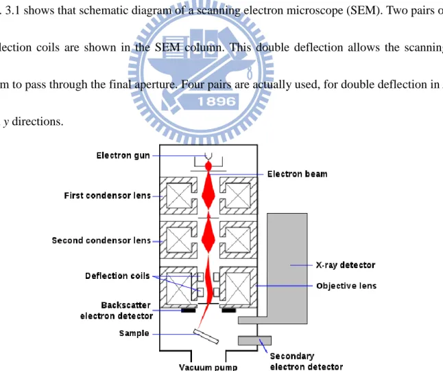
3.1 Scanning electron microscopy (SEM)
The scanning electron microscope is built of the following parts:
(i) The electron gun
(ii) The system of three-stage electromagnetic lens is used to demagnify (focus, condense)
the electron beam diameter to 5~10 nm at the specimen.
(iii) Detectors may detect electrons, X-ray or cathodo-luminescent (CL) light.
(iv) The microscope column is evacuated to 10-5 torr.
Fig. 3.1 shows that schematic diagram of a scanning electron microscope (SEM). Two pairs of
deflection coils are shown in the SEM column. This double deflection allows the scanning
beam to pass through the final aperture. Four pairs are actually used, for double deflection in x
and y directions.
26
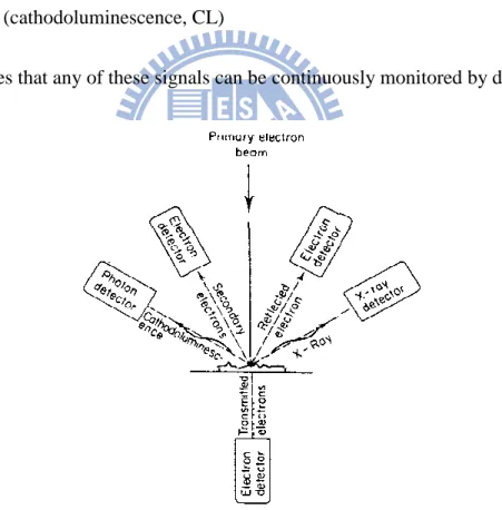
SEM is a technique which forms an image of microscopic region of the specimen surface.
An electron beam from 5~10 nm in diameter is scanned across the specimen. The interaction
of the electron beam with the specimen produces a series of phenomena such as:
(i) backscattering of electrons of high energy
(ii) secondary electrons of low energy
(iii) absorption of electrons
(iv) X - ray
(v) visible light (cathodoluminescence, CL)
Fig. 3.2 indicates that any of these signals can be continuously monitored by detectors.
Fig. 3.2 Information that can be generated in the SEM by an electron beam striking the sample.[2]
27
3.2 Cathodoluminescent spectroscopy (CL)
Cathodoluminescence (CL) is a SEM-based technique that can be used for analyzing the
characteristic of semiconductor materials and devices. CL is the emission of light as the result of electron or “cathode-ray” bombardment. SEM-based and CL can provide information on the concentration and distribution of luminescent centers, distribution and density of
electrically active defects, and electrical properties including minority carrier diffusion
lengths and lifetimes.
28
3.3 Atomic Force Microscopy (AFM)
Atomic force microscopy (AFM) or scanning force microscopy (SFM) is a very
high-resolution type of scanning probe microscopy (SPM) instead of optical imaging one. In
1986, the AFM was invented by Gerd Binnig, Christoph Gerber, and Calvin F. Quate. The
AFM is one of the foremost tools for imaging, measuring, and manipulating matter at
the nanoscale. A very tiny, pyramidal probe is attached on the cantilever. The tip must be very
tiny (single atom size) with sharp angle for large-area scan.
The AFM utilizes a sharp probe moving over the surface of a sample in a raster scan. When
the probe is approaching sample surface, attractive (van der Waals force) or repulsive force
(Coulomb repulsion) between tip and sample is formed and detected. Forces between the tip
and the sample lead to a deflection of the cantilever according to Hooke's law. The interaction
force causes cantilever to shift along z-axis and thus the topology of sample is obtained. The
small probe-sample separation (on the order of the instrument’s resolution) makes it possible
to take measurements over a small area. To acquire an image the microscope-scans the probe
over the sample while measuring the local property in question. The resulting image
resembles an image on a screen in that both consist of many rows or lines of information
placed on above the other. Unlike the traditional microscopes, scanned probe system do not
use lenses, so the size of the probe rather than diffraction effect generally limits their
29
Followings are the operating mode of AFM, shown as the Figs. 3.4[(a)-(c)]:
1. Contact mode: The Interaction mainly comes from repulsive force between tip and sample.
It is easy to obtain atomic-scale resolution, but easy to damage surface of sample.
2. Non-contact mode: The Interaction mainly comes from van der Waals force between tip
and sample. The tip never touches sample surface; resolution is lower (~50 nm). The
surface of samples is preserved.
3. Tapping mode: The tip touches the surface of samples periodically. The resolution could
be as high as contact-mode. The surface of samples could be damaged sometimes.
(a) (b)
(c)
Figures. 3.4[(a)-(c)] Operating mode of AFM (a) contact mode, (b) non-contact mode, (c) tapping mode.[2]
30
3.4 Micro photoluminescence spectroscopy (µ-PL)
Photoluminescence (PL) spectroscopy has been used as a measurement method to detect
the optical properties of the materials because of its nondestructive characteristics. PL is the
emission of light from the material under optical excitation. Reducing the laser beam spot size
to micrometer by beam expanders and objective lens is the so-called µ-PL. Fig 3.5 illustrates
the photoluminescence process. The laser light source used to excite carriers should have
large energy band gap than the semiconductors. When the laser light absorbed within the
semiconductors, it should excite the carriers from the valence band to the conduction band.
Then, is produces the electrons in the conduction band and the holes in the valance band.
When the electron in an excited state returns to the initial state, it will emit a photon whose
energy is equal to energy difference between the excited state return and the initial state,
31
32
3.5 Electroluminescence spectroscopy (EL)
Electroluminescence (EL) is an optical and electrical phenomenon in which a material
emits light in response to an electric current passed through it, or to a strong electric field
across the material. This is different from light emission resulted from chemical reaction
(chemiluminescence), or other mechanical action (mechanoluminescence).
Electroluminescence is the result of radiative recombination of electrons and holes in the
material such as semiconductor. The excited electrons release their energy as photons – light.
Prior to recombination electrons and holes are separated either as a result of doping of the
material to form a p-n junction such as LED, or through excitation by impact of high energy
electrons accelerated by a strong electric field (as with the phosphors in electroluminescent
33
3.6 Reference
[1] http://en.wikipedia.org/wiki/File:Schema_MEB_(en).svg [2] Class of Materials analysis, S. H. Yang, NCTU in Tainan
34
Chapter 4 Result and discussion
4.1 Fabricate LED on the GaN epilayer of defect selective passivation
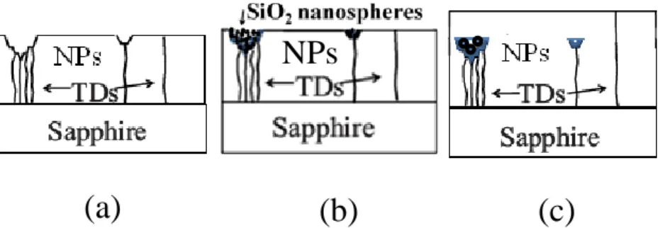
Figs. 4.1[(a)-(d)] shows the previous process flow of defect selective passivation. In Fig.
4.1(a), the molten KOH or hot H3PO4 selectively etch defect sites and form hexagonal pits on
GaN surface. To block the propagation of threading dislocation, a 500nm SiO2 film was
deposited on the GaN in Fig. 4.1(b) Then, the SiO2 thin film on the flat surface is removed by
chemical mechanical polishing (CMP). Meanwhile, the SiO2 in the defect pits still remain
untouched as shown in Fig. 4.1(c). The exposed GaN flat surface provides the seed layer for
epitaxial regrowth, which grows in both vertical and lateral direction to cover over the SiO2
passivated pits as shown in Fig. 4.1(d).
The previous process of DSP method is complex and expensive equipment. In this thesis,
we do something different from previous process. Figs. 4.2[(a)-(c)] show the schematic of the
simplified process. First, the GaN wafers with native pits (NPs) are chosen shown as Fig.
4.2(a). Then we use the SiO2 nanospheres as mask to block defect pits in GaN epitaxial
growth. The process of defect selective blocking by self-assembled silica nanospheres
performed through the spin coating method without expensive setup.
The LED structure with 2μm Si-doped n-GaN, 12pairs of InGaN/GaN multi-quantum
wells(MQWs), and 30nm Mg doped p-GaN were grown on the template. The QW emission
35
on GaN defect pits, and a LED coated 100nm silica nanospheres on GaN pits denoted as
sample A, B, C, respectively.
4.2 Analysis of defect selective passivation process
Wet chemical etching is commonly used for estimating defects density and defect types. In
order to reveal the etched pits from dislocation in GaN and look for any consistency among
the various chemical etches, we have used hot H3PO4 and molten KOH as defect etchants in
GaN, which produce hexagonal-shaped etch pits. By varying the time and temperature, the
etching process produces a pitted surface that clearly reveals the size and density of the pits
that we need to know. Fig. 4.3 shows that the properties of etch pits depend upon the solution
temperature and etched time. When immersing specimen in solution at long time and high
temperature, there are often several pits clustered together. Moreover, chemicals overetch the
GaN plate.
Surface morphology of samples was characterized by scanning electron microscopy (SEM)
and atomic force microscopy (AFM). The SEM image of the GaN sample etched by H3PO4
for 2 min at 240 °C is shown in Fig. 4.4[(a),(b)]. The etch pits, with a density of about
9.58×105 cm-2, are of hexagonal shape and their size ranges from 1.50 to 1.88μm in diameter.
Etch pits might be related with threading screw dislocations or nanopipes (open core
36
Figure 4.5[(a),(b)] shows that the surface morphology of the GaN sample grown by the
same run immersed in molten KOH for 2min30sec at 300°C. The size of the etch pits is about 1μm, and the density of etched pits is 106
cm-2. The EPD of the sample etched by KOH is ten
times higher than that found for the H3PO4-etched sample. Three different shapes of the etch
pits were identified with three types of defects originated from screw-, edge-, and mixed-type
TDs, respectively. It has been realized that dislocation etch pits etched by molten KOH to
identify the origin and mechanism of etch pits in GaN layer[3].
Fig. 4.6(a) indicates that the the defect pits density of GaN with native pits is
approximately 105~106 cm-2. Then the Fig. 4.3(b) shows that a pit is filled with nanospheres.
37
Figs. 4.2[(a)-(c)] Schematic diagrams of simplified defect selective passivation process
Fig. 4.3 Optical microscopy image of GaN surface etched at varied time and temperature.
(c)
(a)
NPs
38
Fig. 4.4 SEM image of GaN surface etched by H3PO4. Low (a) and high (b) magnification images.
Fig. 4.5 SEM image of GaN surface etched by molten KOH. Low (a) and high (b) magnification images.
Figs. 4.6[(a),(b)] SEM image of GaN surface spin-coated nanospheres. Low (a) and high (b) magnification images.
39
4.3 Analysis of DSP-LED performance
4.3.1 Optical properties analysis of LED grown on DSP epilayer
Photoluminescence(PL)
A LED without DSP process, a LED coated 40nm silica nanospheres on GaN defect pits,
and a LED coated 100nm silica nanospheres on GaN pits denoted as sample A, B, C,
respectively. The LED structure with 2μm n-GaN, 12pairs of InGaN/GaN multi-quantum
wells(MQWs), and 30nm p-GaN were grown on the template. The room temperature
photoluminescence spectra at 10mW pumping power are shown as Fig. 4.7. The MQWs
emission wavelength ranges about at 440nm. The intensity of sample B and C are two or three
times than that of sample A. From the result, we think that the crystal quality of GaN epilayer
grown with DSP process has been effectively improved.
400 420 440 460 480 500 0 5000 10000 15000 20000 25000 30000 35000 40000 45000
PL
In
tensity (a.
u.
)
Wavelength (nm)
Reference 40nm 100nm40
Cathodoluminescent (CL)
The optical characteristic is investigated by SEM cross section and cathodoluminescent
images as shown in Figs. 4.8[(a)-(f)]. These images are taken by simply switching detection
mode from scattering electron detection to cathodoluminescent detection under the same
magnification condition and thus have one to one location correspondence. Comparing to the
cross section CL image of different samples, A, B and C, respectively, the DSP methed
minimizes the propagation of threading dislocations.
CL plane-view images as observed in Figs. 4.9[(a)-(c)]. The dark spots are corresponding
with dislocations. We estimate the density of dark points on different samples, 8.24×107 cm-2
at sample A, 5.24×106 cm-2 at sample B and 2.94×106 cm-2 at sample C. It clearly reveals that
the nanospheres effectively block the propagation of threading dislocations but also reduce
the density of defect pits. The threading dislocation defects are the strong non-radiative
recombination centers[4]. The significant increase in CL intensity demonstrates that the loss
of excited carriers due to non-radiative recombination is greatly reduced in the defect
passivated layer as a result of reduction in TD density.
4.3.2 Electrical properties analysis of LED grown on DSP epilayer
LED chips with size of 300×300 μm2 were fabricated from the defect selective passivation
41
same fabrication process except for the defect passivation structure. The light-current (L-I)
and voltage-current (V-I) curves of LEDs are shown in Fig. 4.11. Furthermore, the optical
power was collected by an integrating sphere to make sure that radiation in all directions was
collected. The L-I curve in Fig. 4.11 indicates that the optical output power of DSP-LEDs are
much higher than that of reference-LED. The silica masks not only block the propagation of
threading dislocation but also act as light scattering sites which reduce light trapped by total
internal refection (TIR) to enhance light extraction efficiency. Between the reference-LED
and DSP-LED passivated by 40nm SiO2 nanospheres, the output power of DSP LED exhibits
46%, 39%, 25% and 18% enhancement at 50mA, 100mA, 150mA and 200mA, respectively.
Meanwhile, the output power exhibits 45%, 38%, 25% and 17% enhancement at respectively
50mA, 100mA, 150mA and 200mA, when comparing reference-LED and DSP-LED
passivated by 100nm SiO2 nanospheres.
Fig. 4.12 shows the reverse voltage versus current characteristics of DSP-LEDs and
ref-LED. The leakages come from the non-radiative recombination of screw type dislocations.
As observed in Fig. 4.12, we believe that the defect passivation process does not introduce
more screw defects[5]. As the above mentioned, the defect selective passivation method can
42
Sample A (a) (d)
Sample B (b) (e)
Sample C (c) (f)
Figs. 4.8[(a)-(f)] [(a)-(c)] SEM and [(d)-(f)] CL cross section image of the defect selective passivatied epi-wafer under the same magnification.
43
(a) Sample A
(b) Sample B
(c) Sample C
44
(a)
(b)
Figs. 4.10[(a)-(b)] CL spectrum of (a) plane-view and (b) cross section LED structure.
350 400 450 500 550 600 0 5000 10000 15000 20000 25000 30000 35000 40000 CL I ntensi ty (a. u. ) Wavelength (nm) Ref. 40nm 100nm
PMT:900V
410 420 430 440 450 460 470 0 500 1000 1500 2000 2500 CL I ntensi ty (a. u. ) Wavelength (nm) Ref. 40nm 100nm 340 360 380 400 420 440 460 480 500 0 20000 40000 60000 80000 100000 120000 Ref. 40nm 100nm CL I ntensi ty (a. u. ) Wavelength (nm)PMT:850V
45
Fig. 4.11 L-I and V-I curve of DSP-LEDs and ref-LED.
Fig. 4.12 Leakage current of DSP-LEDs and ref-LED under reverse bias.
0 50 100 150 200 250 0 1 2 3 4 5 6 Current (mA)
Vol
tage (V)
0.00 0.25 0.50 0.75 1.00 1.25 1.50 1.75 2.00 Reference 40nm 100nmIn
tensity (a.
u.
)
46
4.4 Reference
[1] S.K. Hong*,1, B.J. Kim, H.S. Park, Y. Park, S.Y. Yoon, T.I. Kim, J. Cryst. Growth, 191
(1998).
[2] S. K. Hong, T. Yao, B. J. Kim, S. Y. Yoon, and T. I. Kim, Appl. Phys. Lett. 77, 82 (2000). [3]L. Lu, Z. Y. Gao, B. Shen,F. J. Xu, S. Huang, Z. L. Miao, Y. Hao, Z. J. Yang, G. Y. Zhang, X. P. Zhang, J. Xu, and D. P. Yu, J. Appl. Phys, 104, 123525 (2008).
[4] T. Hino, S. Tomiya, T. Miyajima, K. Yanashima, S. Hashimoto, and M. Ikeda, Appl. Phys. Lett., 76, 3421 (2000)
[5] J. W. P. Hsu, M. J. Manfra, R. J. Molnar, B. Heying, and J. S. Speck, Appl. Phys. Lett. 81,
47
Chapter 5 Conclusion & Future work
In summary, we successfully simplify the process of defect selective passivation technique
by choosing the GaN wafer with native pits and spin-coating silica nanospheres on GaN
surface. This technique can effectively not only block the propagation of threading
dislocations but also improve the crystal quality of GaN epilayer. Eventually, we use the GaN
epilayer dealt with defect selective passivation technique to fabricate high efficient LED.
There are some further studies listed in the following:
1. Exploring additional chemical solution that is complementary to KOH in defect selective
etching to increase the coverage rate of defect selective passivation. Same passivation
process needs to be investigated before sending the wafer back to MOCVD for GaN
epitaxial growth.
2. To measure the beam profile of LED at the operating current is the other further work. Try
![Fig. 2.2 Radiative and non-radiative recombination in active region. [21]](https://thumb-ap.123doks.com/thumbv2/9libinfo/8254101.171811/28.892.156.773.524.967/fig-radiative-non-radiative-recombination-active-region.webp)
![Fig. 2.4 Total internal reflection in GaN-based LED. [21]](https://thumb-ap.123doks.com/thumbv2/9libinfo/8254101.171811/29.892.315.639.513.923/fig-total-internal-reflection-gan-based-led.webp)
![Fig. 2.5 The angle of total internal reflection defines the light-escape cone. [21]](https://thumb-ap.123doks.com/thumbv2/9libinfo/8254101.171811/30.892.308.643.138.466/fig-angle-total-internal-reflection-defines-light-escape.webp)
![Fig. 2.7 Schematic diagrams of the cross section GaN film viewed along [-1-120] direction for N-polar GaN to explain the mechanism of the polarity selective etching](https://thumb-ap.123doks.com/thumbv2/9libinfo/8254101.171811/31.892.209.716.123.960/schematic-diagrams-direction-explain-mechanism-polarity-selective-etching.webp)
![Fig. 3.5 Interband transitions in photoluminescence system.[3]](https://thumb-ap.123doks.com/thumbv2/9libinfo/8254101.171811/41.892.205.718.116.741/fig-interband-transitions-in-photoluminescence-system.webp)
![Figure 4.5[(a),(b)] shows that the surface morphology of the GaN sample grown by the same run immersed in molten KOH for 2min30sec at 300°C](https://thumb-ap.123doks.com/thumbv2/9libinfo/8254101.171811/46.892.127.802.486.934/figure-shows-surface-morphology-sample-grown-immersed-molten.webp)