用CMOS 0.25µm來完成一個適用藍芽規格具I/Q四相位輸出除整數架構之頻率合成器及探討次諧波混頻器在無線通訊方面的應用
73
0
0
全文
(2) 用 CMOS 0.25µm 來完成一個適用藍芽規格具 I/Q 四相位輸出除整數 架構之頻率合成器及探討次諧波混頻器在無線通訊方面的應用 A Fully Integrated I/Q Integer-N Frequency Synthesizer for Bluetooth and A Research In Sub-Harmonic Mixer For Wireless Application in 0.25µm CMOS. 研究生:陳政良. Student:Chen, Jheng-Liang. 指導教授:周復芳 博士. Advisor:Dr. Christina F. Jou. 國立交通大學 電信工程學系碩士班 碩 士 論 文 A Thesis Submitted to Institute of Communication engineering College of Electrical Engineering and Computer Science National Chiao Tung University In Partial Fulfillment of the Requirements For the Degree of Master of Science In Communication Engineering July 2004 Hsinchu, Taiwan, Republic of China 中 華 民 國 九 十 三 年 七 月.
(3) 用 CMOS 0.25µm 來完成一個適用藍芽規格具 I/Q 四相位輸出除整數 架構之頻率合成器及探討次諧波混頻器在無線通訊方面的應用. 研究生:陳政良. 指導教授:周復芳 博士. 國立交通大學 電信工程學系 碩士班. 摘要 本論文包含兩部分工作。第一部分我們實現了一個適用藍芽規格具 I/Q 四相 位輸出除整數架構的頻率合成器。我們先由電路中壓控振盪器設計起,將它設計 成能產生四相位輸出。在除頻器部分,我們採用除整數的架構以提供較少的功率 消耗為低電流操作考量。 頻率合成器的量測結果如下所列:振盪頻率可調範圍在 2392~2514MHz 之 間,鎖定所需時間約在 100µsec,距主頻 1MHz 遠處之相位雜訊為-102dB/Hz, 寄生雜頻較主頻低 40dB;使用 2.5V 電壓源時消耗功率為 35.19mA。 第二部分我們介紹了一個主動雙重對稱式的次諧波波混頻器。模擬結果顯示 當在 RF 端灌入 5.2MHz 的訊號經由混頻在 IF 輸出端 20MHz 處可得 11dB 的電 壓增益。混頻器在 5.2GHz 的 IIP3 模擬結果為-4dBm,1dB 壓縮點在-13dBm。 用 2.5V 的電壓源混頻器電路核心消耗 2mA 的電流而輸出緩衝器消耗 8mA。 電路應用的範圍在無線通訊直接升降頻的收發機上。這兩個設計都是用 0.25um CMOS 的技術來完成。 I.
(4) A Fully Integrated I/Q Integer-N Frequency Synthesizer for Bluetooth and A Research In Sub-Harmonic Mixer For Wireless Application in 0.25µm CMOS. Student: Chen, Jheng-Liang. Advisor:Dr. Christina F. Jou. Institute of Communication National Chiao Tung University. Abstract This thesis contents two works. First, we implement a fully I/Q Integer-N Frequency Synthesizer for Bluetooth application. We begin from the design of voltage controlled oscillator (VCO), devising it to generate quadrature phase output. In the design of frequency divider part, we adopt integer-N topology which provides a less power consumption for low current use consideration. The measurement results are listed as following: the oscillation frequency is tunable between 2392~2514MHz, locking time is approximately 100µs, phase noise is -102dBc/Hz@1MHz offset, spurious tones are less than carrier 40dB; the power consumption is 35.19mA using a 2.5V power supply. Second, we describe an active double-balance sub-harmonic mixer. The simulated conversion gain at an RF input of 5.2GHz with IF output at 20MHz is 11dB.The mixer has a simulated IIP3 of -4dBm and an input 1dB compression point of -13dBm at 5.2GHz. The mixer core consumes 2mA of current and the output buffers consume 8mA current using a 2.5V power supply. The application areas are in direct conversion transceivers for wireless system. Two designs are all implemented in 0.25µm CMOS technique.. II.
(5) 誌 謝 首先要感謝指導教授周復芳老師給我的關心與鼓勵,以及博士班 鄭國華學長的建議和督促,讓我可以順利畢業。 當然也要感謝實驗室的同窗好友盈昌、炳宏、汪揚以及學弟政 宏、家良、欽賢、偉成、柏達、俊賢們在設計、量測電路上給予我的 幫助。 此外,還要特別感謝電子所那宗霖、致遠、旻珓、丁彥同學在我 遇到問題時給予不少協助,還好有電子所那邊雕刻機的幫忙,讓我能 確定晶片是沒問題的,而有繼續量測下去的勇氣。另外則是在我心情 不好時陪我打電動娛樂。 最後,謝謝我的父母、家人、還有以上不及備載的諸位好友們, 今日之我是你們合力所造就完成,由衷的感謝各位。是你們,在我平 淡無奇的人生旅途中,劃下了一道道絢麗的光彩。. III.
(6) CONTENTS CHINESE ABSTRACT………………………………………….……..I ENGLISH ABSTRACT………………………………….……………II ACKNOWLEDGMENT…………………………………..…………III CONTENTS…………………………………………………………..IV TABLE CAPTIONS……………………………………….………….VI FIGURE CAPTIONS………………………………………………..VII. Chapter 1 INTRODUCTION……………………….………..…….1 1.1 Background and motivation……………………….…………………….1 1.2 Thesis organization…………………………………..……………...6. Chapter 2 FREQUENCY SYNTHESIZER……………………………...8 2.1 Architectures………………………………………..……………………8 2.2 VCO design………………………………………………………………9 2.2.1. Design issues and introduction……………...………………9. 2.2.2. Simulation results of VCO……………………….…….……12. 2.3 Fully Programmable Frequency Multi-Modulus Divider……14 2.3.1. Design issues and introduction……………………………14. 2.3.2. Simulation results of Divider………………………16. 2.4 Phase/Frequency Detector…………………………………………18 2.5 C har ge P u m p… … . . … … … … … … … … . … … … … … … … … … 2 2 IV.
(7) 2.6 Loop Filter and Loop Bandwidth Considerations………………23 2.7 Simulation results of whole frequency synthesizer…………27. Chapter 3 M e a s u r e m e n t R e s u l t s … … … … … … … … … 3 1 3.1 Measurement Considerations………………………………………..31 3.2 VCO Measurement Results…………………………………………33 3.3 Whole Circuit Measurement Results……………………………39 3.4 Summary of Measurement Results…………………….………………44 3.5 Measurement Discussions………………………….……………45. Chapter 4 S u b - h a r m o n i c M i x e r … … … … … … … … … … . 5 1 4.1 Architectures………………………………….………….………51 4.2 Sub-Harmonic Mixer Core Circuit………………………………51 4.3 Quadrature Phase Generator………………………..………………52 4.4 Simulation Result of Sub-Harmonic Mixer……….………………….53 4.5 Comparison to Fundamental Mixer…………………..………………57. Chapter 5 CONCLUSIONS AND FUTURE PROSPECTS…….58 5.1 Conclusions…………………………………………..…………………58 5.2 Future prospects………………………………………………………59. REFERENCES…………………………………………………………60. V.
(8) TABLE CAPTIONS Table. 1.1. Frequency synthesizer comparator…………………2. Table. 1.2. Mixer comparator…………………………..…………4. Table. 2.1. Loop filter elements………………………………………………26. Table. 3.1. Summary of specifications……………………………………44. Table. 3.2. DC current consumption……………………………………45. Table. 3.3. Loop filter elements……………………………………50. Table. 4.1. Performance Summary………………………………………...56. Table. 4.2. Comparison of sub-harmonic mixer to fundamental mixer…..57. Table. 5.1. Measurement data compared to spec requirement……...58. VI.
(9) FIGURE CAPTIONS Fig. 1.1 Block diagram of a typical transceiver without channel selection. filter……………………….……..……...5. Fig. 1.2 Down/up conversion of signal…………………..…………………6 Fig. 2.1 The architecture of integer-N frequency synthesizers…………9 Fig. 2.2 ( a ) Q u a d r a t u r e p h a s e V C O s c h e m a t i c … … … … … … … . 1 0 (b) Four inverters cascade to generate quadrature phase……11 Fig. 2.3 Simulated output transient waveform………………………………12 Fig. 2.4 Simulated tuning curve…………………………………………13 Fig. 2.5 Simulated phase noise at oscillation frequency 2.448GHz………13 Fig. 2.6 (a) Traditional prescaler and Program, Swallow counter…….…14 (b) Fully programmable frequency divider………….…..……14 Fig. 2.7 Differential source coupled logic………………………………...16 Fig. 2.8 Frequency divider simulate divide by 31 output waveform……17 Fig. 2.9 Frequency divider simulated with VCO………………….……17 Fig. 2.10 (a) PFD block diagram (b) PFD state diagram(c) PFD timing diagram…………………………………………………….…18 Fig. 2.11 (a) Conventional PFD circuit (b) Modified PFD without dead zone…………………..…….……………………………...….20 Fig. 2.12 P F D c h a r a c t e r i s t i c … … … … … … … … … . … … . . . … … … … … 2 1 Fig. 2.13 L i m i t a t i o n c a u s e d b y d e a d z o n e … … … … … . … … … … … 2 1 Fig. 2.14 Charge pump………………………………………………………22 Fig. 2.15 Linear model of PLL……………………………………………………23. VII.
(10) Fig. 2.16 T h i r d. order. loop. filter………….……………24. Fig. 2.17 P L L l o o p f i l t e r d e s i g n s o f t w a r e … … … … … . … . . … 2 6 Fig. 2.18 F r e q u e n c y s y n t h e s i z e r b u i l d i n g b l o c k s … . . . … 2 7 Fig. 2.19 ( a ) L o c k i n g t r a n s i e n t s i m u l a t i o n e l e m e n t v a l u e s of loop filter from hand calculation(2448MHz) (b) Locking transient simulation element values of loop filter from simulation…………………………………………28 Fig. 2.20 Locking spectrum simulation (2480MHz)………………………29 Fig. 2.21 Whole frequency synthesizer layout…………………….……30 Fig. 2.22 W h o l e c h i p d i e p h o t o … … . . … … … … … … … . … … 3 0. Fig. 3.1 Measurement instruments r(a) 8563E spectrum analyzer(b) 54602A oscilloscope(c) E3611A power supply……………….…………31 Fig. 3.2 P C B l a y o u t … … … … … … … . … … … … … … . … … … … 3 2 Fig. 3.3 T e s t i n g. board…………………………..…………33. Fig. 3.4 The open loop Spectrum of frequency synthesizer…………………34 Fig. 3.5 Measured tuning range of VCO under different bank conditions…35 Fig. 3.6 Measured tuning range of VCO compared with simulation……36 Fig. 3.7 Measured tuning range of VCO compared with re-simulation……37 Fig. 3.8 The layout circuit for quadrature phase measurement (a)The layout of quadrature generator(b)The layout of whole circuit……………...….38 Fig. 3.9 (a) Measured locking spectrum at 2400MHz.………………39 (b) Measured locking spectrum at 2401MHz.………………40 (c) Measured locking spectrum at 2448MHz.………………40 (d) Measured locking spectrum at 2449MHz.………………41 (e) Measured locking spectrum at 2480MHz.………………41 VIII.
(11) (f ) Measured locking spectrum at 2481MHz.………………42 Fig. 3.10 Measured phase noise of frequency synthesizer…………………43 Fig. 3.11 L o c k i n g t r a n s i e n t o f 2 4 8 0 M H z m o d e … … … … … … … 4 3 Fig. 3.12 Hopping transient between 2448 and 2480MHz….……………44 Fig. 3.13 P r o t e c t i o n c i r c u i t … … … … … … … . . … … . . … … … … … … … 4 6 Fig. 3.14 Measuring board (a) Testing board before (b) Testing board after modification………………………………………………..…46 Fig. 3.15 (a) Spectrum of frequency synthesizer without bypass capacitor….47 (b) Phase noise of frequency synthesizer without bypass capacitor..48 Fig. 3.16 Phase error simulation(a) Bond wire effect simulation(b) Phase error of S21………………………………………………..……….….49 Fig. 3.17 The settling time using arbitrary loop filter values(a) Measured settling time(b) Simulated settling time……..…………………50 Fig. 4.1 The schematic of Gilbert Cell Mixer and Sub-Harmonic Mixer (a) Traditional Gilbert Cell Mixer (b) Sub-Harmonic Mixer……………………………………………………………..…52 Fig. 4.2 Poly-phase filter circuit…………………….…………………….53 Fig. 4.3 Layout of. even harmonic mixer………………………………53. Fig. 4.4 I F o u t p u t w a v e f o r m … … … … . … … … … . … … … … … … … 5 4 Fig. 4.5 RF input frequency versus conversion gain……………..………55 Fig. 4.6 Two tone test of. IIP3………………..………………..………56. Fig. 4.7 Double sideband noise figure……………………..……………56. IX.
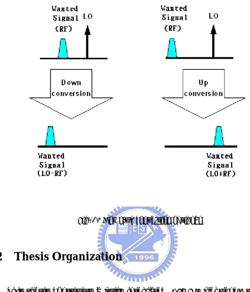
(12) Chapter 1 INTRODUCTION. 1.1 Background and Motivation There is a growing demand for wireless communication in today’s world. The expansion of the market for portable wireless communication devices has given tremendous push to the development of a new generation of radio frequency integrated circuits (RFIC) products. As research over the recent years, the CMOS technology has become the essential design targets for the communication ICs due to the property of low-cost, low power consumption and highly integration. Based on the above reason, the works are all implemented with TSMC 0.25-µm CMOS process to build up 2.4GHz frequency synthesizer and 5GHz sub-harmonic mixer.. In RF transceiver, frequency synthesizer is one of the key components. Frequency synthesizer actions as a local oscillator (LO) and converts signals from base band to radio frequency or inversely (Fig. 1.1, Fig. 1.2). Wireless system has demands on stringent specifications, such as high sensitivity, narrow channel spacing, large output power and low bit error etc. These -1-.
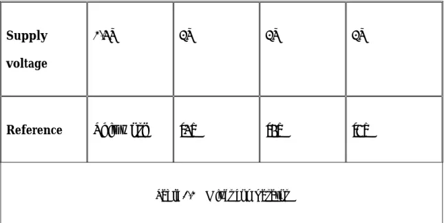
(13) demand can refer to the performance requirement of frequency synthesizer, such as low phase noise, low spur level, high frequency resolution, fast settling time. Besides, we require a frequency synthesizer with accurate quadrature signal phase to perform image rejection for integration consideration. So the design of synthesizer remains one of the challenging blocks in RF systems because it must meet very stringent requirement. Recently, there are many works focusing on frequency synthesizer. Table 1.1 lists this work compared with that ones.. Center. 2.4GHz. 2.4GHZ. 2.4GHz. 2.4GHz. 25μsec. N.A. 120μsec. frequency. Settling time 100μsec. Phase Noise. -102dBc@1MHz -88dBc@1MHz -97dBC@1MHz -125dBC@3MHz. Power. 32.5mW+. 58.6mW. 49.5mW. 15mW. 2.5V. 3.3V. 1.8V. consumption 55mW(buffer). Supply. 2.5V. voltage. -2-.
(14) Technology. Frequency. CMOS. CMOS. CMOS. CMOS. 0.25μm. 0.25μm. 0.35μm. 0.18μm. 2.39~2.51GHz. 2.34~2.53GHz. 2.4~2.5GHz. 2.26~2.66GHz. range. Reference. This work. [1]. [2]. [3]. Table 1.1 Frequency synthesizer comparator. In 5GHz wireless LAN, the use of direct-downconversion techniques is a promising approach for highly integrated wireless receivers due to their potential for low-power fully monolithic operation and extremely broad bandwidth. However, second-order distortion, 1/f noise, and local oscillator self-mixing are the most vexing problem of the architecture [4]. Sub-harmonic mixer provides an excellent solution to the above problems. However, sub-harmonic mixers have historically been implemented in millimeter-wave technology as a means of performing downconversion of the received signal with an LO operating at a fraction of the frequency of the input signal. In the thesis, we attempt to implement the sub-harmonic mixer with TSMC 0.25-µm CMOS process for 5GHz wireless LAN application. Table 1.2 lists the -3-.
(15) sub-harmonic mixer compared with recent ones.. Conversion. 11dB. 13dB. 11.6dB. 18dB. Noise Figure. 14dB. 24.5dB. 12dB. 8dB. IIP3. -4dBm. -10.6dBm. -13.5dBm. -6.6dBm. P1dB. -13dBm. -19.9dBm. N.A. N.A. LO frequency 2.615GHz. 450MHz. 1005MHz. 1.1GHz. RF frequency. 5.25GHz. 900.05MHz. 2012.2MHz. 2.1GHz. Tech. CMOS. CMOS. CMOS. SiGe BiCMOS. 0.25μm. 0.35μm. 0.25μm. 0.35μm. 5mW(core). 5.16mW. 5.1mW. 12.6mW. Gain. Power Consumption. -4-.
(16) Supply. 2.5V. 3V. 3V. 3V. This work. [5]. [6]. [7]. voltage. Reference. Table 1.2 Mixer comparator. Fig. 1.1 Block diagram of a typical transceiver without channel selection filter. -5-.
(17) Fig. 1.2 Down/up conversion of signal. 1.2 Thesis Organization This thesis constructs a fully integrated 2.4GHz frequency synthesizer and a 5GHz sub-harmonic mixer by TSMC CMOS 0.25-µm technology.. Chapter 2 introduces synthesizers’ architectures, simulation information, system bandwidth considerations and designing tips.. Chapter 3 presents the measurement results of each building block of the frequency synthesizer, and of course the measured data of whole system.. Chapter 4 introduces sub-harmonic architectures, simulation information, and designing tips.. -6-.
(18) Finally, we discuss our measurement results, self-criticisms of the shortcomings in specifications, and future prospects in Chapter 5.. -7-.
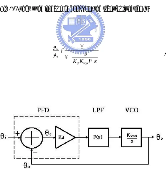
(19) Chapter 2 FREQUENCY SYNTHESIZER. 2.1 Architectures In this chapter, we discuss about all the functional blocks in integer-N frequency synthesizer and how to design them. Fig 2.1 presents the architecture of integer-N frequency synthesizer. The frequency synthesizer contains five functional blocks, including voltage controlled oscillator(VCO), divider, phase frequency detector(PFD), charge pump and low pass loop filter(LPF). Except the reference oscillator and LPF, all blocks are done on chip. We separate the power supplies of all the blocks in order to avoid substrate cross talk and for testing consideration [8]. functional blocks latter.. -8-. We will discuss how to design all.
(20) Fig. 2.1 The architecture of integer-N frequency synthesizers. 2.2 VCO Design 2.2.1 Design Issues and Introduction VCO is the core circuit in the frequency synthesizer. In most RF design, we use LC-tank oscillator instead of ring oscillator for better phase noise. For image cancellation, we hope VCO can provide quadrature phase output signal. There are three ways to generate quadrature signals: divide-by-two circuit [9]; RC-polyphase network [1]; and two VCOs cross connect with each other [10]. Using divide-by-two circuit needs to design a VCO operate at the double frequency of original frequency. VCO operating at higher frequency will consume more power and have poor phase noise. Besides, this structure also shows poor quadrature accuracy because of the requirement of 50% duty cycle VCO. A VCO with RC-polyphase network consumes less power than others, but RC-polyphase is signal power hungry. Besides, the bandwidth of RC-polyphase is too small to cover the band from 2400MHz to 2481MHz. -9-.
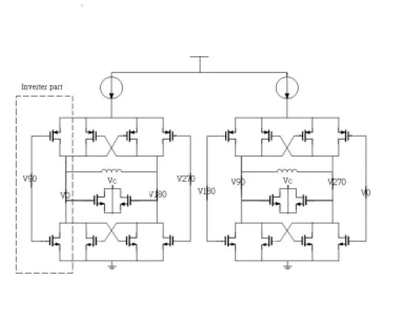
(21) Based on the former reasons, we choose two VCOs cross connect with each other here to generate quadrature signal which have accurate quadrature phase signal and large output signal power. The whole schematic of the quadrature VCO is shown in Fig. 2.2(a). The architecture of cross-coupled pairs adopts both NMOS and PMOS transistors to enhance negative conductance and LC-Resonator to conclude the resonance frequency. Four inverters cascade to create quadrature phase output as Fig. 2.2(b) shows.. Fig. 2.2(a) Quadrature phase VCO schematic. - 10 -.
(22) Fig. 2.2 (b) Four inverters cascade to generate quadrature phase. When designing the frequency range of VCO, large tuning range enhances the sensitivity of VCO to substrate noise. However, small tuning range is hard to cover the band of Bluetooth from 2.4~2.483GHz. In order to guarantee the whole tuning range of implemented VCO is exactly as we require, we add capacitor banks at the two ends of LC-tank. This can help us to adjust the tuning range of the implemented chip.. This design adopts 3 sets of capacitor bank, i.e. there’s three control bits and enables us to set the oscillator under 6 operating conditions: 000, 001, 010, 011, 100, 101, and 111. Different control bit is connected to different amount of parallel capacitors; higher bit is connected to a larger capacitance. When a control bit of capacitor bank is at high level, the capacitor is enabled and the capacitance of LC-tank is increased.. Bank design gives a stronger guarantee to avoid the shifting of oscillating frequency, however, it worsen the phase noise of VCO due to the turn on - 11 -.
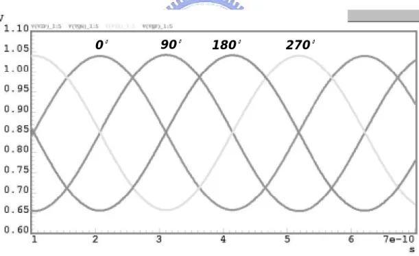
(23) resistance of switch MOS [1].. 2.2.2 Simulation Results of VCO The simulated output transient waveform of VCO is shown as Fig. 2.3. In the design, the phase error is almost zero if no device mismatches. Fig. 2.4 shows the tuning range of the VCO at bank 100 is approximately linear from frequency 2.4~2.483GHz which implies a constant KVCO in the operation range; it is an advantage for phase-locked loop. Fig. 2.5 shows the simulated phase noise at oscillation frequency 2.448GHz. At 3MHz offset from the carrier, phase noise is -120dBc/Hz. This specification satisfies Bluetooth standard.. 0°. 90°. 180°. 270°. Fig. 2.3 Simulated output transient waveform. - 12 -.
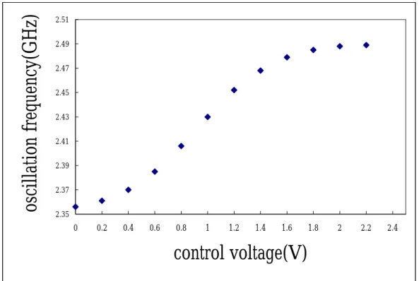
(24) oscillation frequency(GHz). 2.51 2.49 2.47 2.45 2.43 2.41 2.39 2.37 2.35. 0. 0.2. 0.4. 0.6. 0.8. 1. 1.2. 1.4. 1.6. 1.8. 2. control voltage(V) Fig. 2.4 Simulated tuning curve. Fig. 2.5 Simulated phase noise at oscillation frequency 2.448GHz. - 13 -. 2.2. 2.4.
(25) 2.3 Fully Programmable Frequency Multi-Modulus Divider 2.3.1 Design Issues and Introduction. Fig. 2.6(a) Traditional prescaler and Program, Swallow counter. Fig. 2.6(b) Fully programmable frequency divider. Fig. 2.6 (a) shows the traditional prescaler with two counters to perform - 14 -.
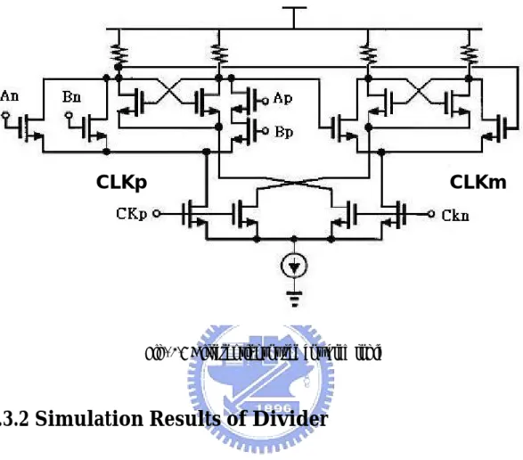
(26) frequency divider. However, the extendibility of this architecture is low for having to determine the divide number of P-counter and S-counter for different range of divider. Fig. 2.6(b) presents another architecture which we adopt in this work [16]. It is composed by 11 cascaded dual modulus asynchronous divide-by-2/3 circuits. This architecture only requires change the number of divide-by-2/3 block for different range of divider. This design assures only the first two stages of the divider operate at the frequency over GHz. We can set divide modulus N by changing the input level of each program bits (b0, b1, b2…). In this work, divider can be programmed to all integers between 2048 and 4095, depending on the input bits b0 to ba. [11]: 10. N = 2048 + ∑ bn ⋅ 2n n=0. (2.1). Frequency divider is a critical part besides VCO due to its high operating speed. The maximum operating frequency is limited by the parasitic capacitance of the layout connection path and the load of the first stage to the second one. In order to reach a maximum operating frequency at 2.5GHz, the first two stages are realized in a differential Source Coupled Logic (SCL) and we scale down the NMOS transistor size of the second stage to minimize the first stage’s capacitor load. Carefully choosing the transistor sizes and accurately counting the parasitic capacitor are all critical to the correct operation of divider. Fig 2.7 is the SCL circuit which works as a high speed NAND-DFF.. The following 9 stages are realized with digital cells which can operate at frequency up to several hundred MHz and consume less power than the first - 15 -.
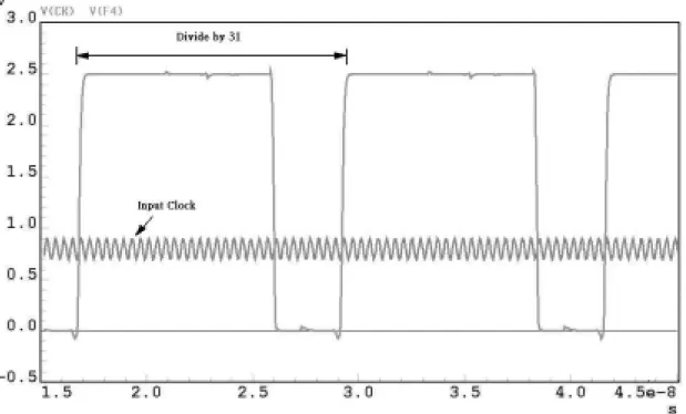
(27) two stages.. CLKp. CLKm. Fig. 2.7 Differential source coupled logic. 2.3.2 Simulation Results of Divider Simulating 11 stages of dual modulus asynchronous divide-by-2/3 circuit takes long time. So we first take the first five stages to simulate. Fig. 2.8 shows the simulation result of divide by 31. We see the input clock even with 0.25 V peak to peak swing and frequency up to 2.6GHz still working well.. - 16 -.
(28) Fig. 2.8 Frequency divider simulate divide by 31 output waveform. The. co-simulation. result. of. fully. programmable. frequency. multi-modulus divider and VCO is as shown in Fig. 2.9. The VCO output frequency is set at 2448MHz and the divide modulus is set at 2448, too. We can obviously observe the period of output divided signal is 1µs, this figures out our divider is working regularly.. 1µs. - 17 -.
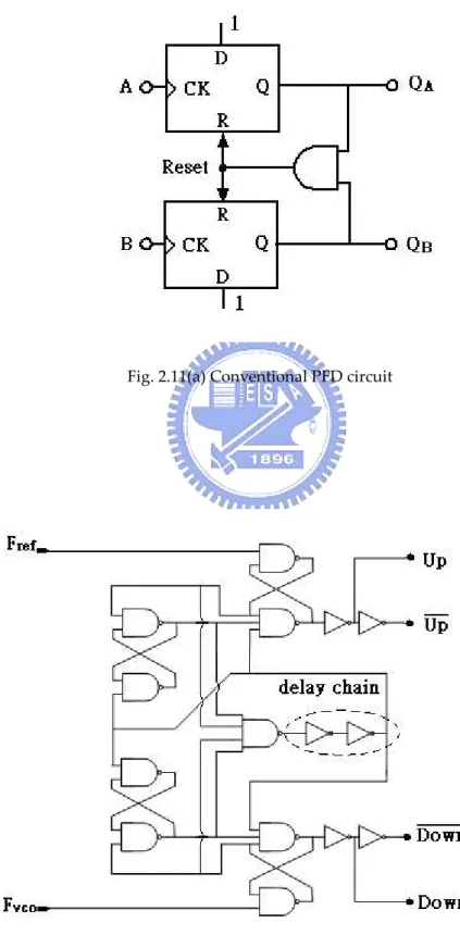
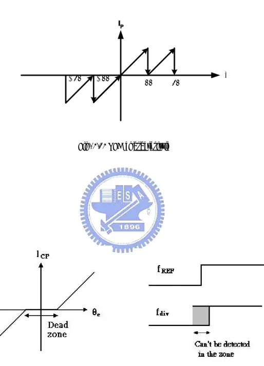
(29) Fig. 2.9 Frequency divider simulated with VCO. 2.4 Phase/Frequency Detector Phase frequency detector can detect both phase and frequency difference between the reference signal and the output signal of the frequency divider. As shown in Fig. 2.10, if the frequency of input A is greater than that of B, QA is high, but QB is still low. On the contrary, if the frequency of input B is greater than that of A, QB is high, but QA is still low. If the frequency of A equals that of B, the circuit will check the phase difference between the two inputs and generate a pulse that equals the phase difference at QA or QB.. Fig. 2.10 (a) PFD block diagram. Fig. 2.10 (b) PFD state diagram. - 18 -.
(30) Fig. 2.10 (c) PFD timing diagram. In the thesis, we choose three state phase/frequency detector (PFD) for detecting both phase and frequency difference. Fig 2.11(a) shows the conventional circuit of three state PFD circuit. The circuit consists of two D-flip flops and an AND gate. We set the initial condition of the two D-flip flops’ output QA=QB=0. If B=0 but A is from 0 to 1, then QA=1 until B is also from 0 to 1 which makes QB becomes high and resets the two D-flip flops to low. The PFD’s characteristic is ideally linear for the entire range of input phase differences from -2π to 2π as Fig. 2.12 shows. When the inputs differ in frequency, the phase difference changes each cycle by 2π((TCKref -TCKout)/max(TCKout,TCKref)). On. every. clock. cycle. during. frequency. acquisition, the phase differences steps across the PFD transfer curve from 0 to ±2π and repeats as the output clock cycle slips. So the control voltage of VCO is pumped monotonically toward that of the desired frequency.. However, the conventional PFD circuit has the drawback of dead zone existed when it incorporates with charge pump. The dead zone generates phase jitter since the control system does not change the control voltage when the phase error is within the dead zone as Fig2.13 shows. Fig. 2.11(b) shows - 19 -.
(31) the PFD realized in this thesis. The delay inverter chain used in the circuit which increases the delay of reset signal can eliminate dead zone [12].. Fig. 2.11(a) Conventional PFD circuit. - 20 -.
(32) Fig. 2.11 (b) Modified PFD without dead zone. IP. − 4π. − 2π. 2π. 4π. Fig. 2.12 PFD characteristic. Fig. 2.13 Limitation caused by dead zone. - 21 -. ∆θ.
(33) 2.5 Charge Pump The charge pump [11] (Fig. 2.14) adopted in this thesis works with a fixed reference current. To achieve a high voltage output range at the charge pump, the transistor size of the current mirror transistors (M1-M11) must be chosen carefully. Also an accurate layout of the charge pump is important to improve the matching of the positive and negative current to avoid mismatch currents. Mismatch currents produced when the two phase are compared cause reference spur. Reference spur interferes with adjacent channel in RF receiver and it also produces undesired spectral emission in RF transmitter. We implement two additional transistors (M12, M14) to guarantee in case of switching the transistors M13 and M15, their sources are already precharged. Above reduces current peaks during the switching time and suppressing the spurious tones, too.. Fig. 2.14 Charge pump. - 22 -.
(34) 2.6 Loop Filter and Loop Bandwidth Considerations The characteristic of PLL helps frequency synthesizers partially alleviate their phase noise contributed by VCO. Extending the bandwidth of PLL can reduce phase noise in band of the loop and increase the settling time of the whole loop. However, a wide band PLL suffers from higher level of spurious tones. The loop filter can determine the bandwidth of PLL by introducing poles and zeros in the close phase locked loop. The poles help degrade the magnitude of reference spur and the zeros help PLL have enough phase margin to guarantee the close loop’s stability.. Fig 2.15 shows the linear model of PLL, the transfer function is:. θo = θe 1 +. 1 s K d K vco F ( s ). - 23 -. (2.2).
(35) Fig. 2.15 Linear model of PLL. We use 3rd order passive loop filter in this design. Fig. 2.16 shows a standard third order loop filter used in most synthesizers. The filter comprises a second order filter section and an R2 and C3 section to provide an extra pole to assist the attenuation of the side bands at multiples of the comparison frequency that may appear. However, extra pole may make the whole loop unstable. So, the design of loop filter is critical.. Fig. 2.16. Third order loop filter. The element value of loop filter can be determined on the following step [13].. First, we have to choose the loop bandwidth of PLL. The locking time of the Bluetooth application is 200-usec.We assume the locking time Ts=100-usec(for a over design). Two “rule of thumb”[25], which may help to approximate the frequency - 24 -.
(36) of the loop bandwidth, are. Switching ...time ≈. Switching ...time ≈. 50 f comparison. 2 .5 f loopbandwidth. (2.3). (2.4). From equation 2.3, the estimated comparison frequency is ≧500kHz. Our reference frequency is 1MHz which satisfies the requirement. Equation 2.4 predicts an estimated loop bandwidth≧25kHz in order to achieve lock in time.. C2 =. R1 = 2 ⋅ ρ ⋅. K vco ⋅ I cp 2 ω BW ⋅N. N K vco ⋅ I cp ⋅ C 2. (2.6). C2 12. (2.7). R1 ⋅ C 2 20 ⋅ R2. (2.8). C1 =. C3 =. (2.5). Based on above equations, we can obtain a set of element values. Besides, we can get another set of element values from the loop filter simulation tool shown in Fig. 2.17. The values are all listed in Table 2.1:. The two set element values slightly differ because the hand calculate do - 25 -.
(37) some approximation when analysis. We will see the approximation will not have much influence on the settling time of whole circuit in section 2.7.. Fig. 2.17 PLL loop filter design software. Calculated. Result. Simulated Result. C1. 5pF. 6.5pF. C2. 60pF. 138pF. R1. 212kΩ. 139kΩ. C3. 1pF. 0.6pF. R2. 636kΩ. 740kΩ. Table 2.1 Loop filter elements. - 26 -.
(38) 2.7 Simulation results of whole frequency synthesizer Finally, all the building blocks mentioned in previous sections and chapter are combined to be a whole frequency synthesizer and simulated together as Fig. 2.18 shows. Because frequency synthesizer circuit contains many sub-circuits, simulating the settling time from circuit level takes a lot of time. So at first, we use ADS tool to perform behavioral simulation of frequency synthesizer’s settling time and then use eldoRF to verify whether the connections of whole loop are correct or not.. Fig. 2.18 Frequency synthesizer building blocks. We use different element values of loop filter derived from above section to simulate and the outcome in Fig. 2.19 shows the settling time is less than 200µs as the spec of Bluetooth required. Fig. 2.20 shows the close loop spectrum of VCO.. - 27 -.
(39) Fig. 2.19(a) Locking transient simulation element values of loop filter from hand calculation(2448MHz). Fig. 2.19(b) Locking transient simulation element values of loop filter from simulation. - 28 -.
(40) tool(2448MHz). 2480MHz. Fig. 2.20 Locking spectrum simulation (2480MHz). Fig. 2.21 and 2.22 show the layout and the die photo of whole chip. The die size is 1400µm×950µm.. - 29 -.
(41) Fig. 2.21 Whole frequency synthesizer layout. 1400µm. 950µm. Fig. 2.22 Whole chip die photo. - 30 -.
(42) CHAPTER 3 MEASUREMENT RESULTS. 3.1 Measurement Considerations This work is measured on PCB, the measurement instruments include 8563E spectrum analyzer and 54602A oscilloscope as Fig 3.1 shows.. (b) 54602A oscilloscope. (a) 8563E spectrum analyzer. (c ) E3611A power supply Fig. 3.1 Measurement instruments. - 31 -.
(43) Fig. 3.2 shows the PCB layout and the testing board of the chip. The chip is stuck on testing PCB, and wires are bonded from the pad on chip to feed bias voltages. We use a DIP switch to switch the VCO capacitor Bank and divider. An off-chip 1MHz oscillator instead of function generator is used to produce reference clock for suppressing the noise coming from reference frequency. The loop filter is also designed out of chip for easily modifying element values and decrease chip area although it introduces more noise than designed fully on chip.. Fig. 3.2 PCB layout. - 32 -.
(44) Fig. 3.3 Testing board. 3.2 VCO Measurement Results The measured spectrum and tuning range of VCO used in this work is shown from Fig. 3.4 to Fig. 3.5. The tuning range of Bank(100) covers the band from 2.4GHz to 2.483GHz as we desire. Fig. 3.6 shows the tuning range of measurement data compared with simulation results. The chips are discovered falling on SF corner from WAT data provided by TSMC, so we re-simulation with this condition.. The measured tuning range is 2.392 ~ 2.514GHz, comparing with our simulation results which is 2.288~2.411GHz at TT corner and 2.343~2.478GHz at SF corner. There are approximately 40~50MHz frequency differences - 33 -.
(45) between measurement and simulation. That means the parasitic effects are evaluated more than reality. With careful examination, we find the parasitic capacitor of RFMOS has been evaluated twice. Besides, the frequency using two VCO connected to each other is more sensitive to corner variation than that only using one VCO.. Fig. 3.4 The open loop Spectrum of frequency synthesizer. - 34 -.
(46) Fig. 3.5 Measured tuning range of VCO under different bank conditions. - 35 -.
(47) Fig. 3.6 Measured tuning range of VCO compared with simulation. After re-simulating the tuning range with reducing the parasitic capacitor of VCO resulting from RFMOS, we can get better fit of the measurement data with simulation results as Fig. 3.7 shows.. - 36 -.
(48) Fig. 3.7 Measured tuning range of VCO compared with re-simulation. We use quadrature generator to measure the phase error of VCO output signal. Fig. 3.8 shows the layout of quadrature generator. The s-matrix of quadrature generator is [14]: 0 j 1 0 j 0 0 1 [s] = − 1 2 1 0 0 j 0 1 j 0 . (3.1). - 37 -.
(49) (a)The layout of quadrature generator. (b)The layout of whole circuit. Fig. 3.8 The layout circuit for quadrature phase measurement. When the phase of input signal of port 1 is θ˚ and port 4 is ψ˚, port1 port2 having phase difference roughly 90˚, we can get the s-parameter of port2 and port3 as formulation from 3.2 to 3.4 presents.. 1. Port2= −. 2. 1. Port3= −. P3 =( P2. − −. 2. 1 2 1 2. ( je jθ + e jφ ) = −. 1. (e jθ + je jφ ) = −. 1. [1 + e jθ e ]e jφ. [1 − e. )2 ~ ( jθ e. ] je. jφ. 2. 2. [1 − e jθ e ]e jφ. (3.2). [1 + e jθ e ] je jφ. 2 2 ) sin θ e. - 38 -. (3.3). (3.4).
(50) The measurement shows the output power of port2 is -25dBm and the output power of port3 is -10dBm. From formula 3.4, we can deduce the phase error between port2 and port3 is 20˚.. 3.3 Whole Circuit Measurement Results The measurement data of whole synthesizer are shown in following figures. Fig. 3.9 are the output spectrum when synthesizer are locked at 2400, 2401, 2448, 2449, 2480, 2481MHz.. -40dB. Fig. 3.9 (a) Measured locking spectrum at 2400MHz. - 39 -.
(51) -40dB. Fig. 3.9(b) Measured locking spectrum at 2401MHz. -40dB. Fig. 3.9(c) Measured locking spectrum at 2448MHz. - 40 -.
(52) -40dB. Fig. 3.9(d) Measured locking spectrum at 2449MHz. -40dB. Fig. 3.9(e) Measured locking spectrum at 2480MHz. - 41 -.
(53) -40dB. Fig. 3.9(f) Measured locking spectrum at 2481MHz. Fig. 3.9 shows the output signal power of the frequency synthesizer has approximately 2dB variation from 2.4GHz to 2.481GHz and the reference spur of the frequency synthesizer is -40dB which satisfies the spec of Bluetooth requires.. Fig. 3.10 presents the close loop phase noise of frequency synthesizer which is -102dBC/Hz at 1MHz offset. Fig. 3.11 is the waveform of VCO input control voltage, it represents the locking transient waveforms of the synthesizer. The locking settling time shown is less than 200µs.. - 42 -.
(54) -102dBC/Hz. Fig. 3.10 Measured phase noise of frequency synthesizer. Locking transient of VCTR. VCO Power on. Fig. 3.11 Locking transient of 2480MHz mode. - 43 -.
(55) Fig. 3.12 is the frequency hopping transient between 2448 and 2480MHz mode. We adopt function generator to feed a low frequency square wave as mode switching. The hopping settling time is less than 200µs.. 2480 mode. 2448 mode. Fig. 3.12 Hopping transient between 2448 and 2480MHz. 3.4 Summary of Measurement Results The measured data in this chapter are summarized in Table. 3.1 and 3.2.. Simulation. Measurement. Power supply. 2.5V. 2.5V. Tuning range of VCO. 2.373 ~ 2.513GHz. 2.392 ~ 2.514GHz. - 44 -.
(56) Phase noise. -108dBc/Hz@1MHz. -102dBc/Hz@1MHz. Spurious tones. N/A. -40dB. Locking time. About 80µs. About 100µs. Table. 3.1 Summary of specifications. Block. Simulation. Measurement. VCO. 4mA. 3.72mA. Buffer. 20mA. 22mA. Frequency divider. 6.4mA. 6.7mA. Charge pump. 2.8mA. 2.7mA. Rest parts of PLL. 0.63mA. 0.07mA. Total. 33.83mA. 35.19mA. Table. 3.2 DC current consumption. 3.5 Measurement Discussions The chip manufactured using TSMC 0.25-µm CMOS process suffers from the problem of ESD severely. The gate oxide breaks down easily with inexact operation procedure and without protection circuits. We should give voltage on the gate of PMOS first then increasing voltage on the source side gradually, conversely, give voltage on the source of NMOS first then increasing gate side gradually when turn on the bias circuits. Besides, for decreasing the circuits damaged by pulse, we should add protection circuits at each gate side of biasing circuits as Fig. 3.13 shows. - 45 -.
(57) Fig. 3.13 Protection circuit. The power lines of the testing circuits are also a critical topic to the performance of measurement. Digital or analog power supply is noisy power source, so we add bypass capacitors from 1uF, 1nF, to1pF as near the pad of chip as possible to suppress the noise coming from power source. Besides, adding more via between the top and bottom of the test board and using GSG layout on the power lines and bias lines all can help get more stable bias. Fig. 3.14 shows the testing board with and without the stability equipment.. (a) Testing board before. (b) Testing board after modification. Fig. 3.14 Measuring board. Fig. 3.15(a) shows that the spectrum of the frequency synthesizer without bypass capacitor is more unstable and noisy than with pure power source. Fig. - 46 -.
(58) 3.15(b) measures the phase noise which is even -88dBC/Hz, -14dB worse than with pure power source.. Fig. 3.15 (a) Spectrum of frequency synthesizer without bypass capacitor. - 47 -.
(59) Fig. 3.15 (b) Phase noise of frequency synthesizer without bypass capacitor. The measuring phase error of quadrature phase is 20° worse than simulation. After analysis, we find the bond wire from the pad to the testing board will induce much phase shift and influence the measuring result. If we assume the chip inside and line of testing board all match to 50 Ω, using Microwave office tool to simulate the length of bond wire with 1µm variation shows that there will be 7° phase difference caused bond wire as Fig. 3.16 shows. Besides, the bond wire causes unbalance LO power in port1 and port4. There is approximately 28° phase error if the power difference between two ports is 1dB.. There is another reason for bad phase error: the isolation port of - 48 -.
(60) quadrature generator is only -20dB at 2.4GHz which will have some power leakages from port1 to port4, reversely from port4 to port1 and degrade the ability of image cancellation. Moreover, the testing board actually is difficult to match to 50Ω for bond wire consideration. After we calibrate the phase error due to the LO input power difference which is approximate 0.4dB, bond wire length variation which is roughly 1µm, quadrature generator phase error which is about 2°, the phase error can be less than 1° in really. So, the best way to get the accurate phase error is to design a mixer circuit inside of the chip to down convert the frequency to lower frequency to reduce the bond wire effect.. (a) Bond wire effect simulation. (b) Phase error of S21. Fig. 3.16 Phase error simulation. When measuring the settling time of frequency synthesizer, we try to use arbitrary element values of loop filter to see the impact on the settling time. Fig. 3.17 shows the settling time compared with simulation using arbitrary element values as listed in table 3.3. The result points out that the settling time may be larger than 200µsec if using unsuitable filter values. Besides, using too long wire connecting to the VCTR will make the settling time longer than - 49 -.
(61) 200µsec, too.. Element. value. C1. 47pF. C2. 470pF. R1. 15kΩ. C3. 47pF. R2. 15kΩ. of. loop. filter. Table.3.3 Loop filter elements. (a) Measured settling time. (b) Simulated settling time. Fig. 3.17 The settling time using arbitrary loop filter values. - 50 -.
(62) Chapter 4 Sub-harmonic Mixer. 4.1 Architectures In this chapter, we give the approach to the even-harmonic mixer, present our analysis, and show its post simulation performance. Finally, we compare the even-harmonic mixer with the traditional Gilbert cell mixer.. 4.2 Sub-Harmonic Mixer Core Circuit Fig 4.1(a) shows the traditional Gilbert cell mixer which can be divided into two part where M1、M2 are as RF signal amplifier and they also can increase the LO to RF signal isolation ; M3-M6 is the actual frequency mixing part. The even-harmonic mixer is modified from Gilbert cell mixer which only replaces mixing mode MOS to differential pair as fig. 4.1(b) shows [5]. The CMOS even-harmonic mixer provides down conversion mixing of the differential RF input signal with even harmonic of the LO differential signal while suppressing RF mixing with the LO fundamental and odd harmonics. As shown, suppression of odd harmonic mixing is accomplished by summing - 51 -.
(63) the differential signals at. the drains of M3、M4, M5、M6, M7、M8, and M9、. M10. The quadrature ~ FRF/2 signal applied to the LO inputs also allows the RF signal to be switched on every quarter cycle of the LO drive waveform, creating an effective 2*F lo signal. The inductor L1 is used to produce a pole at 5GHz to increase mixer conversion gain and L2 L3 is for RF input matching.. (a)Traditional Gilbert Cell Mixer. (b) Sub-Harmonic Mixer. Fig. 4.1 The schematic of Gilbert Cell Mixer and Sub-Harmonic Mixer. 4.3 Quadrature Phase Generator For measurement consideration, we use poly-phase filter to generate quadrature phase for LO input [15]. A simplified schematic of the poly-phase filter is shown in Fig. 4.2. The poly-phase filter outputs phase and amplitude vary with LO input frequency. Nevertheless, the LO quadrature signals maintain a 90 o phase difference and the same amplitude over a wide - 52 -.
(64) bandwidth. We can use 2-ord poly-phase filter to increase circuit bandwidth. However, this will decrease the LO signal power further.. Fig. 4.2 Poly-phase filter circuit. 4.4 Simulation Result of Sub-Harmonic Mixer The even harmonic mixer has been fabricated using TSMC 0.25-µm mixed-signal CMOS process. The final layout of fully integrated Mixer is shown in Fig. 4.3.. Fig. 4.3 Layout of even harmonic mixer. - 53 -.
(65) All elements are fully integrated on a chip including spiral inductors, metal-insulator-metal (MIM) capacitors, multi-finger RF NMOS transistors, poly resistors and decouple MOS capacitors. The total chip size including the pads is about 850umx850um. At high frequencies, the drain and source of a MOSFET, pads, inductors, and other element on the Silicon (Si) substrate have resistive components due to resistivity of the Si substrate. These parasitic resistances consume signal power, generate thermal noise, and thus noise performance of the mixer is degraded a lot. To avoid these effects from pads, we use shielding PAD at RF、LO input and IF output to reduce coupling noise from the noisy Si substrate. [16]. Fig. 4.4 shows the simulation output waveform of mixer. The high frequency component can be removed by off-chip filter.. Fig. 4.4 IF output waveform. - 54 -.
(66) Fig. 4.5 shows the result of mixer conversion gain versus RF input frequency with the LO input frequency from 2.5GHz to 2.7GHz and an LO input power of 3dBm and IF frequency of 20MHz is selected.. A two tone test. is performed to measure the input third order inter-modulation point of the mixer. The two tones are at 5.2GHz and 5.205GHz resulting in fundamental tones at 20MHz and 25MHz , and third order intermods at 15MHz and 30MHz at the IF output.. Fig. 4.5 RF input frequency versus conversion gain. Fig. 4.6 shows the fundamental and intermod powers with respect to the two tone input powers. Extrapolation of the two curves results in an IIP3 of -4dBm.The mixer has a simulated double sideband noise figure of 14dB at an RF frequency of 5.25GHz with the LO input power of 3dBm and IF frequency of 20MHz. Fig. 4.7 shows the mixer double sideband noise figure. Table 4.1 summarizes the post simulation performance.. - 55 -.
(67) Fig. 4.6 Two tone test of IIP3. Fig. 4.7 Double sideband noise figure. Power Supply. 2.5V. RF input frequency. 5.25GHz. LO input frequency. 2.615GHz. Conversion Gain. 11dB. Noise figure. 14dB - 56 -.
(68) IIP3. -4dBm. P-1dB. -13dBm. Mixer Core power. 5mW. Table 4.1 : Performance Summary. 4.5 Comparison to Fundamental Mixer Careful examination of Fig. 4.1(b) will shows that the even harmonic mixer(IF=RF-2*LO) can be converted to a fundamental mixer (IF=RF-LO) by connecting the 0 o and. 180 LO inputs together ,and also the 90 and 270 LO. inputs together. The result is a fundamental LO Gilbert cell mixer whose input stage is identical to the even harmonic mixer. Table 4.2 shows the comparison of the even harmonic mixer to the fundamental mixer. The simulated NF for fundamental mixer is about 3dB lower than the even harmonic mixer and conversion gain is about 5dB higher than it.. Parameter. Even Harm.. Fundamental. Conversion Gain. 11dB. 16dB. Noise figure. 14dB. 11dB. IIP3. -4dBm. -5dBm. P-1dB. -13dBm. -14dBm. Core power. 5mW. 5mW. Table 4.2: Comparison of sub-harmonic mixer to fundamental mixer. - 57 -.
(69) Chapter 5 CONCLUSIONS AND FUTURE PROSPECTS. 5.1 Conclusions A fully integrated 2.4GHz CMOS frequency synthesizer is demonstrated. Table 5.1 lists the measurement data compared to the spec of Bluetooth requires. The data shows that we achieve the spec requirement of Bluetooth except to phase error. However, this design suffered from strong spurious tones, and consumed large power in VCO buffer.. Measurement. Spec of Bluetooth. Power supply. 2.5V. N.A. Tuning range of VCO. 2.392 ~ 2.514GHz. 2.4~2.481GHz. Phase noise. -102dBc/Hz@1MHz. -120dBc/Hz@3MHz. Spurious tones. -40dB. N.A. Phase error. 20°. 5°. Locking time. About 100µs. 220µs. - 58 -.
(70) Table. 5.1 Measurement data compared to spec requirement. 5.2 Future Prospects There’re several directions for future work. First, a more accurate method must be set to measure the phase error. We should integrate the down conversion mixer to convert the LO signal to lower frequency for decreasing the bond wire effect to the measurement of phase error. Second, the spurious tones are strong and seriously influence the signal. We have some tactics to alleviate this problem, narrow the bandwidth of the loop filter or minimize the interference of crystal oscillator by designing a current matching circuit in Charge Pump. Through the above two ways, spurious tones can be suppressed more effectively. Third, the VCO buffer should be re-designed to lessen power consumption and counterwork process variation.. Besides, the architecture of conventional integer-N frequency synthesizer suffers from many draw back. The limited bandwidth of integer-N frequency synthesizer causes out off band noise from VCO. Large divide number intensifies the in-band noise from the reference and phase detector noises. The architecture of fractional-N frequency synthesizer solves the problems above. Moreover, the settling time can be faster by using fractional-N frequency synthesizer [20]. Therefore, the future research should be focused on the architecture of fractional-N frequency synthesizer.. - 59 -.
(71) REFERENCES [1] Hsien-Cheng Hsieh, “The Design of Low Power Voltage Controlled Oscillator and Fully Integrated 2.4GHz CMOS Integer-N Frequency Synthesizer”, Thesis of Master’s Degree, Institute of communication, NCTU, Taiwan, ROC, JUN 2003. [2] Zhinian Shu, Ka Lok Lee, and Bosco H. Leung, Senior Member, IEEE, “A 2.4-GHz Ring-Oscillator-Based CMOS Frequency Synthesizer With a Fractional Divider Dual-PLL Architecture”, IEEE J. Solid-State Circuit, vol. 39, pp. 452-462, MARCH 2004 [3] Domine M. W. Leenaerts, Senior Member, IEEE, CiceroS. Vaucher, Senior Member, IEEE, Henk Jan Berg veld, Michael Thompson, and Kevin Moore, “A 15-m W Fully Integrated I/Q Synthesizer for Bluetooth in 0.18 µm CMOS”, IEEE J. Solid-State Circuit, vol. 38, pp. 1155-1162, JULY 2003 [4] Liwei Sheng, Jonathan C. Jensen, Student Member, IEEE, and Lawrence E. Larson, Fellow, IEEE, “A Wide-Bandwidth Si/SiGe HBT Direct Conversion Sub-Harmonic Mixer/Down converter”, IEEE J. Solid-State Circuits, vol. 35, pp. 1329-1337, SEPTEMBER 2000 [5] Zhaofeng Zhang, Zhiheng Chen, Jack Lau, “A 900 MHz CMOS balanced harmonic mixer for direct conversion receivers”, Dept. of Electrical Engineering [6] Sher Jiun Fang, See Taur Lee, and David J. Allstot, “A 2GHz CMOS even harmonic mixer for direct conversion receivers”, Dept. of Electrical Engineering [7] Marc Goldfarb, Senior Member, IEEE, Ed Balboni, Member, IEEE, and John Cavey, ”Even Harmonic Double-Balanced Active Mixer for Use in Direct - 60 -.
(72) Conversion Receivers”, IEEE J. Solid-State Circuits, vol. 38, pp. 1762-1766, OCTOBER 2003 [8] S. Pellerano, S. Levantino, Member, IEEE, C. Samori, Member, IEEE, and A. L. Lacaita, Senior Member, IEEE, “A 13.5-mW 5-GHz Frequency Synthesizer With Dynamic-Logic Frequency Divider”, IEEE J. Solid-State Circuits, vol. 39, pp. 378-383, FEBRUARY 2004 [9] Alireza Zolfaghari, Member, IEEE, and Behzad Razavi, Fellow, IEEE, “A low-power 2.4-GHz transmitter/receiver CMOS IC”, IEEE J. Solid-State Circuits, vol. 38, pp. 176-183, FEBRUARY 2003 [10] Gwong-Wai Cheng, “A 5.25GHz Fully Integrated CMOS Quadrature Voltage-Controlled Oscillator”, Thesis of Master’s Degree, Institute of communication, NCTU, Taiwan, ROC, JUN 2002. [11] Detlev Theil, Christian Durdodt, Andre Hanke, Stefan Heinen, Stefan van Waasen, Dietolf Seippel, Duyen Pham-stabner, Klaus Schmacher, “A Fully Integrated CMOS Frequency Synthesizer for Bluetooth “, IEEE J. Solid-State Circuits, JULY 2001. [12] Henrik O. Johansson, ”A Simple Precharged CMOS Phase Frequency Detector”, IEEE J. Solid-State Circuits, vol. 33, pp. 295-299, FEBRUARY 1998 [13] Steve Williamson, ”How To Design RF Circuits-Synthesizer”, IEE journal, 2000. [14] David M. Pozar, “MICROWAVE ENGINEERING”, University of Massachusetts at Amherst [15] Kiran Nimmagadda and Gabriel M. Rebeiz, “A 1.9GHz Double-Balanced Subharmonic Mixer for Direct Conversion Receivers”, Radiation Lab, EECS Department, The University of Michigan, Ann Arbor - 61 -.
(73) [16] Ryuichi Fujimoto, Kenji Kojima and Shoji Otaka, “A 7GHz 1.8-dB NF CMOS Low-Noise Amplifier,” IEEE J. Solid-State Circuits, Vol. 37, pp. 852-856 , July 2002. [17] Joonsuk Lee and Beomsup Kim, “A Low-Noise Fast-Lock Phase-Locked Loop with Adaptive Bandwidth Control,” IEEE J. Solid-State Circuits, Vol. 35, pp. 1137-1145, Aug 2000. [18] Chi-wa Lo, Howard Cam Luong, “A 1.5V 900MHz Monolithic CMOS Fast-Switching Frequency Synthesizer for Wireless Applications”, IEEE journal, JUN 2000. [19] Christopher Lam, Behzad Razavi, “A 2.6-GHz/5.2-GHz Frequency Synthesizer in 0.4-µm CMOS Technology”, IEEE J. Solid-State Circuits, vol.35, pp.788-794, MAY 2000, [20] Tom A. D. Riley, Member, IEEE, Miles A. Copeland, Fellow, IEEE, and Tad A. Kwasniewski, Member, IEEE, “Delta-Sigma Modulation in Fractional-N Frequency Synthesizer,” IEEE J. Solid-State Circuits, vol.28. pp. 553-559, May 1993 [21] Jan Craninckx and Michiel S. J. Steyaert, Senior Member, IEEE, “A 1.75-GHz/3-V Dual-Modulus Divide-by-128/129 Prescaler in 0.7-um CMOS”, IEEE J. Solid-State Circuits, vol. 31, pp. 890-897, July 1996 [22] J. Craninckx, Student Member, IEEE, and Michel S. J. Steyaert, Senior Member, IEEE “A 1.8-GHz CMOS Low-Phase-Noise Voltage-Controlled Oscillator with Prescaler”, IEEE J. Solid-State Circuits, vol. 30, pp. 890-897, December 1995 [23] Smithson, G. “Synthesised Frequency sources in Digital Cellular Handsets”, Microwaves and RF 1997 Conference Proceedings, pp 124-130. - 62 -.
(74)
數據
+7
相關文件
無線射頻識別 (Radio Frequency Identification, RFID) 系統近年來越來越普及,應用範圍如供
無線射頻識別 (Radio Frequency Identification, RFID) 系統近年來越來越普及,應用範圍如供
無線射頻識別 (Radio Frequency Identification, RFID) 系統近年來越來越普及,應用範圍如供
無線射頻識別 (Radio Frequency Identification, RFID) 系統近年來越來越普及,應用範圍如供
無線射頻識別 (Radio Frequency Identification, RFID) 系統近年來越來越普及,應用範圍如供
Microphone and 600 ohm line conduits shall be mechanically and electrically connected to receptacle boxes and electrically grounded to the audio system ground point.. Lines in
傳統的 RF front-end 常定義在高頻無線通訊的接收端電路,例如類比 式 AM/FM 通訊、微波通訊等。射頻(Radio frequency,
我們提出利用讀取器與讀取器間的距離為參數來優化利用分層移除讀取器之方法的最佳 化技術 Distance Based Optimization for Eliminating Redundant Readers (DBO) ,此方法完全
