國 立 交 通 大 學
電 信 工 程 學 系 碩 士 班
碩 士 論 文
操作於弱反轉層場效電晶體之極低功率損耗與
極小面積 CMOS 參考電壓之設計與實現
The Design and Implementation of an Ultra Low Power and
Small Area CMOS Voltage Reference Based on MOSFET
Operated in Weak Inversion Region
研 究 生:林 信 太
指導教授:闕 河 鳴 博士
Voltage Reference Based on MOSFET Operated in Weak Inversion Region
研 究 生:林信太 Student: Shin-Ta Lin 指導教授:闕河鳴 博士 Advisor: Dr. Herming Chiueh
國 立 交 通 大 學 電 信 工 程 學 系 碩 士 班
碩 士 論 文
A Thesis
Submitted to Department of Communication Engineering College of Electrical Engineering and Computer Science
National Chiao Tung University
In Partial Fulfillment of the Requirements For the Degree of
Master of Science in Communication Engineering October 2007 Hsinchu Taiwan 西元二ΟΟ七年十月
操作於弱反轉層場效電晶體之極低功率損耗與
極小面積 CMOS 參考電壓之設計與實現
研究生:林信太 指導教授:闕河鳴 博士 國立交通大學 電信工程學系碩士班中文摘要
本篇論文使用 0.18 微米互補式金氧半標準製程設計並實現一個與溫度無關 的穩定參考電壓源。最近幾年電池供應的系統越來越廣泛使用,隨著這個趨勢, 在設計電路時都要求小面積、低功率、高效能,而很多類比電路都會需要一個穩 定的參考電壓,因此本論文設計一個低功率與小面積的參考電壓去運用在電池供 應的系統中。本電路工作在弱反轉區可用來取代傳統電路中的雙極性電晶體去實 現與溫度無關的參考電壓,其功率消耗只有幾百奈瓦且面積只有幾百平方微米。 另外,溫度範圍也可以從-80℃到 165℃,而其電壓誤差也僅有幾十毫伏特。因 此,本設計可以運用在電池供應的系統去供應一個穩定的參考電壓。The Design and Implementation of an Ultra Low Power and
Small Area CMOS Voltage Reference Based on MOSFET
Operated in Weak Inversion Region
Student: Shin-Tai Lin Advisor: Dr. Herming Chiueh
Department of Communication Engineering National Chiao Tung University
Hsinchu,Taiwan
ABSTRACT
This thesis uses standard CMOS 0.18μm process technique to design and realize a stable voltage reference which does not change with temperature. In the recent years, battery-operated systems are used extensively. Along with this tendency, we demand low-power, small-area, and high performance when designing circuits. Many analog circuits need a stable voltage reference, so the thesis shows a low-power and small-area voltage reference to apply in battery-operated systems. Proposed circuits work in weak inverse region to replace the bipolar devices in conventional circuit and using proposed circuits realize CMOS voltage reference which does not change with temperature. Its power consumption only has several hundred nano-Watt and its area is only several hundred squre nanometer. In addition, the voltage derivation only has several dozens milli-Volt when temperature range is from -80℃ to 165℃. Therefore, proposed architectures can supply a stable voltage reference in battery-operated systems.
誌謝
本論文可以順利完成,首先要感謝我的指導教授闕河鳴博士,他指導我如何 去完成本論文,很多該注意我沒注意的重點,教授都會仔細一步一步的告訴我該 如何去做,適時給予我意見與正確的方向,我覺得老師教導我的不只是如何去完 成一本論文的方法,而是去完成很多做事情的方法,這是我最受益良多的。 再來,我要感謝嘉儀、江俊、俊誼這三位同窗的好朋友,他們幫我很多事情, 不論是課業或是研究都給我莫大的幫助,然後,感謝佐昇學長在研究上總是會指 導我很多重點,他總是會給我有關論文方面的知識與方法;在這研究所生活中, 這實驗室帶給我很多很多東西,讓我兩年多的研究所生活過得相當充實,有大家 的相伴研究所學習生活多采多姿了起來。 最後,我要感謝我家人,沒有他們就沒有今天的我,還有我女朋友宛樺,她 總是在精神上給予我最大的支持,不論遇到任何問題,她都會安慰我、鼓勵我, 真的非常感謝。CONTENTS
Chinese Abstract………...I
English Abstract………..II
Acknowledgements………III
Contents………..IV
List of Tables………...VI
List of Figures………...VII
Chapter 1 Introduction………..1
1.1 Overview of Battery-Operated System……...1
1.2 Motivation……...3
1.3 Organization...4
Chapter 2 Review of Voltage Reference………5
2.1 Background...5
2.2 Conventional Bandgap Reference...7
2.2.1 Bandgap Reference...8
2.2.2 BJT and MOS Comparison...9
2.3 CMOS Voltage References...10
2.3.1 Voltage Mode of VPTAT and VCTAT...12
2.3.2 Current Mode of VPTAT and VCTAT...15
2.3.3 Voltage Reference Uses Parallel Voltages...17
2.3.4 Zero Temperature Coefficient Point (ZTC)…...19
2.3.5 Voltage Reference Uses Non-standard Process...20
2.3.6 Comparison of Voltage Reference...22
Chapter 3 Circuitry Architecture………26
3.1 Design Process……….………..26
3.1.1 Reference Paper………..………..26
3.1.2 VPTAT (Proportional to Absolute Temperature)..………27
3.2 All NMOSFET Voltage Reference (ANVR)…….………31
3.2.1 Principle of ANVR.………...31
3.2.2 Derivation of ANVR…...……….32
3.2.3 Post-Layout Simulation of ANVR………34
3.2.4 Discussion of ANVR………39
3.3 NMOSFET and PMOSFET Voltage Reference (NPVR)………40
3.3.1 Principle of NPVR………...40
3.3.2 Derivation of NPVR….……….41
3.3.3 Post-Layout Simulation of NPVR.………44
3.3.4 Discussion of NPVR………49
3.4 NMOSFET PMOSFET and Capacitor Voltage Reference (NPCVR)…50 3.4.1 Start-up Circuit of NPCVR…...………...50
3.4.2 Power Supply Reject Ratio (PSRR)……….51
3.4.3 Post-Layout Simulation of NPCVR….………53 3.4.4 Discussion of NPCVR………57 3.5 Comparison……….58 3.6 Summary……….60
Chapter 4 Measurement………...61
4.1 Measurement Set-up………..61 4.2 Experimental Result………634.2.1 Experimental Result of ANVR………...63
4.2.2 Experimental Result of NPVR………...66
4.2.3 Discussion of ANVR and NPVR………..69
4.2.4 Comparison of ANVR and NPVR…..………..70
4.3 Summary……….72
Chapter 5 Conclusion and Future Works..……….73
5.1 Conclusion………...73
5.2 Future Works………...74
List of Tables
Chapter 2
Table 2.1: The Comparison between MOS and BJT……….9
Table 2.2: Researches for Voltage Mode of VPTAT and VCTAT………14
Table 2.3: Researches for Current Mode of VPTAT and VCTAT………...17
Table 2.4: Researches of Voltage Reference of Parallel Voltages………19
Table 2.5: Researches of ZTC………...20
Table 2.6: Researches of Voltage Reference of Non-standard Process……….22
Table 2.7: Comparison for Five Kinds of CMOS Voltage References………..23
Table 2.8: Researches for All CMOS Voltage Reference………..23
Chapter 3
Table 3.1: Post-Layout Simulation of ANVR……….………..35Table 3.2: Corners of ANVR Post-Layout Simulation (VREF) ……...39
Table 3.3: Post-Layout Simulation of NPVR………45
Table 3.4: Corners of NPVR Post-Layout Simulation (VREF)………...48
Table 3.5: Comparison between ANVR and NPVR………..50
Table 3.6: Post-Layout Simulation of NPCVR……….53
Table 3.7: Corners of NPCVR Post-Layout Simulation (VREF)………57
Table 3.8: Comparison between NPVR and NPCVR………...57
Table 3.9: Comparison of All Voltage Reference’s Architectures……….58
Chapter 4
Table 4.1: The Derivation for VREF of ANVR………64Table 4.2: Experimental Results of ANVR….………65
Table 4.3: Resistor Variation….………66
Table 4.4: The Derivation for VREF of NPVR………67
Table 4.5: Experimental Results of NPVR….………68
Table 4.6: Process Variation of VREF……….68
Table 4.7: PSRR of NPVR (4pF in output)………69
Table 4.8: Comparison of Post Layout Simulation and Experimental results……...70
List of Figures
Chapter 1
Figure 1.1: Features and Examples of Battery-Operated System………...2
Figure 1.2: Block Diagram of a Battery-Operated System……….3
Chapter 2
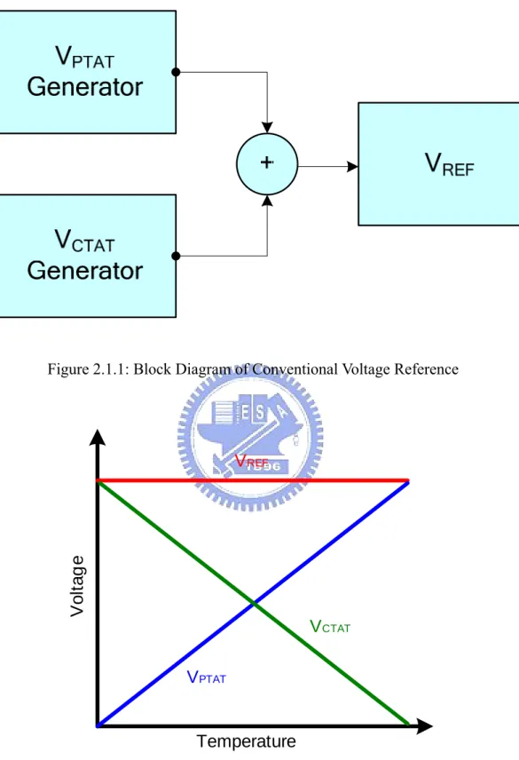
Figure 2.1.1: Block Diagram of Conventional Voltage Reference………..6Figure 2.1.2: The Curvature of VREF Formed by VPTAT and VCTAT………..6
Figure 2.2.1: Conventional Bandgap Reference Circuit….………8
Figure 2.3.1: Circuit Architecture for Voltage Mode of VPTAT and VCTAT (REF[2])..12
Figure 2.3.2: Circuit Architecture for Current Mode of VPTAT and VCTAT (REF[10])……….15
Figure 2.3.3: Circuit Architecture of Parallel Voltages (REF[21])………17
Figure 2.3.4: Circuit Architecture of ZTC (REF[27])………...19
Figure 2.3.5: Circuit Architecture of Non-standard Process (REF[29])………….21
Figure 2.3.6: Vpn and Vnn as a Function of Temperature………21
Chapter 3
Figure 3.1.1: Circuit Architecture of REF[8]……….………...27Figure 3.1.2: Conventional VPTAT Circuit Architecture……….27
Figure 3.1.3: The VPTAT Proposed Architecture……….30
Figure 3.2.1: Architecture of ANVR………31
Figure 3.2.2: Presim of ANVR………...………35
Figure 3.2.3: Layout of ANVR in TSMC 0.18μm CMOS Technology………36
Figure 3.2.4: TT TT_RES Corner of ANVR………...36
Figure 3.2.5: FF TT_RES Corner of ANVR………37
Figure 3.2.6: SS TT_RES Corner of ANVR………37
Figure 3.2.7: SF TT_RES Corner of ANVR………38
Figure 3.2.8: FS TT_RES Corner of ANVR………38
Figure 3.3.1: Architecture of NPVR….………40
Figure 3.3.2: Presim of ANVR………...………44
Figure 3.3.3: Layout of NPVR in TSMC 0.18μm CMOS Technology……….45
Figure 3.3.5: FF Corner of NPVR………...46
Figure 3.3.6: FS Corner of NPVR………...47
Figure 3.3.7: SF Corner of NPVR………...47
Figure 3.3.8: SS Corner of NPVR………...48
Figure 3.4.1: Voltage Reference uses NMOS, PMOS, and Capacitor (NPCVR)….50 Figure 3.4.2: Small Signal of NPCVR………...51
Figure 3.4.3: PSRR of NPCVR………...53 Figure 3.4.4: Layout of NPCVR………...54 Figure 3.4.5: TT Corner of NPCVR………54 Figure 3.4.6: FF Corner of NPCVR………...55 Figure 3.4.7: FS Corner of NPCVR………...55 Figure 3.4.8: SF Corner of NPCVR………...56 Figure 3.4.9: SS Corner of NPCVR………...56
Chapter 4
Figure 4.1: Block Diagram of Measurement Environment………...62Figure 4.2: Block Diagram of Voltage-Stabilized Circuit……….62
Figure 4.3: The Pictures of Measurement Environment………...63
Figure 4.4: Experimental Results of ANVR………64
Figure 4.5: Experimental Results of NPVR………67
CHAPTER
1
Introduction
This chapter will introduce battery-operated system and illustrate motivation. Then, we show that voltage reference is an important circuit in analog circuits and voltage reference needs to become small-area and low-power.
1.1 Overview of Battery-Operated System
In recently these years, battery-operated systems are used widely. For example, cell phone, PDA, GPS, digital watch, notebook, etc, see Figure 1.1. Those give people convenient and support, and those machines will be more and more widespread. Therefore we know that battery-operated system is inseparable with the humanity. Because battery-operated system is already a trend, we should understand battery-operated system. Roughly, battery-operated system has fundamental characteristics which are battery-operated, small-area, portable, and multi-function. Beside, battery-operated systems have a very serious issue which is hot. Now, we will discuss every characteristics in the below parts individually.
1. Battery
Battery-operated systems use battery to supply it working. Battery-operated systems are requested to reach low-power, so the batteries can use longer and save more power. It is good for consumers, because no one want to bring a lot of batteries on body. Therefore designers should take the low power as the goal to design circuit architectures for battery-operated systems.
2. Portable Function
Portable function is convenient for people. Because people can bring powerful electronic products on body and use them anytime and anywhere. Therefore, electronic products want to have portable function, designers should notice that using small-area to design circuit architecture. Using small area and achieving high performance is already a trend at battery-operated systems.
Battery Supply Portable Multi-Function Small Camera DV MP3 NB PDA Cell Phone
Figure 1.1: Feature and Examples of Battery-Operated System
3. Multi-Function
Multi-function means that providing the most functions in a finite area. In other words, multi-function implies system integration and small area. It is very efficient to accomplish in battery-operated system. Therefore, we need to treasure every area by system integration and small circuit architectures which also request high performance.
4. Thermal Issue
Nowadays, battery-operated systems are quite small, and the situation will cause thermal issue. Because a lot of circuit architectures integrate in finite and small area, the heat will increase quickly and be not easy to radiate heat. Therefore battery-operated systems must need smart temperature sensors which can sense
temperature and admonish system. Smart temperature sensors need two voltages which are VPTAT and VREF to compare. And a stable VREF is our goal at
battery-operated system.
In the above introduction, we know that battery-operated systems have some key point which are low-power and small-area and need to solve thermal issue. In the next section, we will explain the motivation of voltage reference at battery-operated system.
1.2 Motivation
Voltage reference is a key element in many circuit architectures. For example, PLL, oscillator, data converter, voltage regulator, DRAM(Dynamic Random Access Menory), flash, and temperature sensor, etc. Those circuit architectures are important and conventional circuit architectures in analog systems. If those want to have high performance, they must need a stable voltage reference which is independent strongly with temperature, process variation, and supply voltage. Therefore, we should not ignore the importance of voltage reference.
It is block diagram of battery-operated system in Figure 1.2. We can know that those above circuits are always used at analog part, power converter, and power management circuit. So, those circuits are designed in battery-operated system, they must need an adaptable voltage reference. It means that a low-power, small-area, and high performance voltage reference is needed in battery-operated systems.
1.3 Organization
Chapter 2 begins with introduction of conventional voltage reference, and three bandgap references are shown and discussed. Then bandgap reference and CMOS voltage reference are compared. Finally, we assort five voltage references of MOS and advance that voltage mode of VPTAT and VCTAT is as our excogitative architecture.
Chapter 3 shows that VCTAT is produced by MOS transistor which works in
subthreshold region and VPTAT is produced by VCTAT. Then proposed design
architectures are implemented and described in detail. Comparison with proposed design architectures and researches is presented finally.
In Chapter 4, measured method and measurement environment are presented. Experimental results for the voltage references fabricated in a standard 0.18-μm CMOS technology are reported and discussed in this chapter.
CHAPTER
2
Review of Voltage Reference
First, this chapter introduces general method of voltage reference. Conventional bandgap references are presented and illustrated. Comparison with bandgap reference and CMOS (Complementary MOS) voltage reference is shown after understanding conventional bandgap references. Then CMOS voltage reference is chosen because it is better than bandgap reference at our design goal. And, CMOS voltage reference is assorted five types at many researches. Finally, choosing voltage mode of VPTAT and
VCTAT is the better adaptable design architecture of voltage reference.
2.1 Background
Nowadays, voltage reference has developed maturely. We can know how to produce voltage reference in many books and researches. And Figure 2.2.1 is block diagram of voltage reference which shows that a stable voltage is produced by two different voltages. In Figure 2.1.2, a traditional VREF which does not change with
temperature is added by VPTAT and VCTAT. If VPTAT and VCTAT are high linearity, VREF
will be a stable voltage. The method is suitable for voltage reference of BJT (Bipolar transistor) or MOS because VCTAT can be produced easily by characteristic of BJT or
MOS, and VPTAT is produced by VCTAT. Underside will show what VPTAT and VCTAT
Figure 2.1.1: Block Diagram of Conventional Voltage Reference
V
PTATV
CTATV
REFTemperature
Vo
lt
a
g
e
If analog circuits want to have a stable voltage reference, two important elements which are VPTAT and VCTAT are needed. CTAT is complementary to absolute
temperature. It means that a voltage decreases with temperature. VCTAT is used to
compensate VPTAT, so VREF will not change with temperature. It is always produced by
VBE of BJT or VGS of MOS which work in subthreshold region. In addition, VCTAT is
also used to produce VPTAT by two different VCTAT which subtract each other.
Therefore, the linearity of VCTAT is important at circuits of voltage reference.
PTAT is proportional to absolute temperature. It means that a voltage increases with temperature. The above paragraph has said that VPTAT is always produced by two
different VCTAT. This is a significant issue how to reach high linearity of VPTAT in
circuits of voltage reference, because it will affect VREF directly. VPTAT is always used
to another purpose which is as a compared voltage in smart temperature sensor. First stage of smart temperature sensor needs two voltages to compare, and the result is an authority of temperature difference which delivers to second stage of smart temperature sensor. Usually, VPTAT is compared with VREF. By this, smart temperature
sensor can have an accurate temperature difference. But, premise is that smart temperature sensor needs high precise VREF and VPTAT.
After knowing the produced method of voltage reference, we need to notice three issues which relate very much to voltage reference. There are supply voltage variation, temperature variation, and process variation. If we can overcome the three issues, a stable voltage reference is produced.
The above principle is often used to produce voltage references, but the principle can derive many different circuits of voltage reference. The traditional voltage reference is designed by BJT, and it is called bandgap reference. In the next section, bandgap reference will be introduced and illustrated.
2.2 Conventional Bandgap Reference
This section will illustrate bandgap reference and show bandgap reference’s architectures. Then a comparison with BJT and MOS is shown and explained. Finally, we choose MOS to design voltage reference because MOS is more suitable to apply in battery-operated system.
2.2.1 Bandgap Reference
Figure 2.2.1: Conventional Bandgap Reference
In Figure 2.2.1, bandgap reference has been shown. M1~M2, Q1~Q2, and operational amplifier is used to produce IPTAT. By mirroring from M2 to M3, we have
the function which is shown as follows,
BE BE CTAT PTAT V V V V + =Δ + = bg V (2-12) And V
( )
n R R VBE T ln 1 2 = Δ (2-13)△VBE is a voltage of positive TC, and VBE is a voltage of negative TC. Then, VREF
will be independent of temperature by adding △VBE and VBE.
After bandgap reference has been illustrated, we will be curious that the difference of voltage reference which use MOS or BJT to design. Why are researches of CMOS voltage reference more and more? What are they advantages and disadvantages? In the next section, we will compare CMOS voltage reference and
bandgap reference. Finding out the advantages and disadvantages of voltage references which are designed by MOS and BJT is very important. Why do we use MOS to design voltage reference, not BJT? The answer will explain afterward.
2.2.2 BJT and MOS comparison
We have understood bandgap reference how to produce in the above section. Now, the focus is that bandgap reference compares with CMOS voltage reference. We list some key points which more important when designing voltage reference. The comparison of voltage references which use MOS or BJT to design is shown in Table 2.1.
Table 2.1: The Comparison between MOS and BJT
MOS BJT
Advantages 1. VTH=0.45V
2. Small area
3. VREF<1.21V, low-voltage
1. Low process variation
2. Low supply voltage variation
Disadvantages 1. Process variation
2. Supply voltage variation
1. VBE=0.6V
2. Large area 3. Vbg=1.21V
Let’s see the advantages of MOS which are also the disadvantages of BJT. First, VTH of MOS is lower than VBE of BJT. We know that MOS operates in subthreshold
region is like VBE which is a voltage of negative TC. It means that VGS has the inverse
ratio with the temperature when VGS < VTH(about 0.45V in TSMC 0.18um process).
Therefore, the same circuit architecture of voltage reference, MOS’s supply voltage is lower than BJT’s supply voltage. In the recent years, a lot of architectures are demanded for low-power, low-voltage, and small-area. The trend is ineluctability and more and more attention, and voltage reference is also following the trend. Therefore, CMOS voltage reference is more ascendant than bandgap reference in low-power architectures.
Second, area of MOS is smaller than area of BJT in the standard CMOS process and the same conditions. So area of voltage reference will decrease when using MOS to design it. The excellence is very useful to design in battery-operated system,
because battery-operated systems usually have some characteristics which are light, small, and portable. Therefore, MOS is easy to reach system integration and decrease the area.
Third, curvature compensation techniques are often used at bandgap reference. Because the linearity of VBE is not very good at overall temperature range, it needs
additional circuit which means curvature compensation techniques to compensate the linearity of Vbg. On the other hand, VTH of MOS has superior linearity, and MOS does
not need curvature compensation technique at wide temperature range. Therefore, the area of voltage reference circuit can be reduced. But, the performance is still good or even better.
Even if MOS has a lot of advantages which is very adaptable in battery-operated system, we still need to attend to process variation when we want to design CMOS voltage reference. Process variation of MOS is more serious than that of BJT, but it can be got over by every corner simulation. We need to run every corner and limit corners at an acceptive range when we simulate voltage reference.
In the above comparison, we know that MOS is better than BJT when designing voltage reference in battery-operated system, so we decide that using MOS to design voltage reference. Before design, we should review researches of MOS voltage reference in the recent six years. Because we can understand how to design CMOS voltage reference by reviewing researches. And it is important to find out advantages and disadvantages from every circuit architectures of voltage reference in researches. The introduction of CMOS voltage reference will be presented in the next section. In addition, we will compare five circuit architectures of voltage reference and choose the best adaptable architecture to discuss in depth.
2.3 CMOS Voltage References
Bandgap reference is a traditional voltage reference. It is formed by VBE of BJT.
VBE is a voltage of negative temperature coefficient, and two different VBE subtract to
produce VPTAT which is a voltage of positive temperature coefficient. So, a stable
voltage reference which is not change with temperature, supply voltage, and process is produced by VPTAT and VCTAT. As the process advances, voltage references request
with the goal at the present age. Therefore, BJT was replaced by MOS when designing voltage reference. The source had been illustrated them in the above sections.
Near present year, someone discover MOS work in subthreshold region has a characteristic which is analogous to BJT. It means that VGS of MOS which works in
subthreshold region is a voltage of negative temperature coefficient. So voltage reference starts to use MOS. In the above sections, we know that MOS has two main advantages. First, it is low voltage, because VGS is lower than VBE. Second, MOS’s
area is small. Because having the two advantages, researches of CMOS voltage references are increasing in the recent six years.
In the recent six years, a lot of researches of CMOS voltage references are designed. CMOS can be assorted five types by those researches. The classified basis is produced method of voltage reference. All types have advantages and disadvantages by themselves. In the following sections, we will illustrate and discuss. Now, the five types are shown below.
1. Voltage Mode of VPTAT and VCTAT:
CMOS voltage reference is produced by IPTAT and VCTAT(VGS).
2. Current Mode of VPTAT and VCTAT:
CMOS voltage reference is produced that IPTAT and ICTAT. IREF multiplies resistor
to produce VREF.
3. Voltage Reference Uses Parallel Voltages:
The circuit uses that two VGS which have the same slope to subtract, then CMOS
voltage reference is produced.
4. Zero Temperature Coefficient Point (ZTC):
When MOS work at a fixed point, the VGS and ID will not change with
temperature. The point is called zero temperature coefficient point. So VGS can
be designed as voltage reference.
5. Voltage Reference Uses Non-standard Process:
CMOS voltage reference which does not use standard CMOS process technique is designed.
The five types will be showed in the below sections. In addition, I choose five researches to illustrate the five types and list the performance of five types. Then the comparison of researches will be shown and discussed. We will illustrate that voltage mode of VPTAT and VCTAT is more suitable than other architectures to design voltage reference in battery-operated system.
2.3.1 Voltage Mode of V
PTATand V
CTATFigure 2.3.1: Circuit Architecture for Voltage Mode of VPTAT and VCTAT (REF[2])
In the last few years, CMOS voltage reference’s circuits can work under 1V. But, those circuits present a high level of complexity. It may cause undesirable behavior and a high quiescent current. Consequently, efforts have been made to develop a simple circuit of voltage reference which has a power supply lower than the bandgap voltage.
The circuit refers to Ref [2]: A CMOS Voltage Reference Based on Threshold Voltage for Ultra Low-Voltage and Ultra Low-Power. It is assorted to voltage mode of VPTAT
and VCTAT. Voltage reference uses only resistors and transistors working in weak
0.35μm TSMC CMOS process. VREF is 514mV for a power supply of 900mV, and
temperature coefficient is 39 ppm/℃ for temperature range from 0℃ to 100℃. (Ref: [2])
The derivative is as follows:
All MOS operate in subthreshold region, and the function is (2-14) (2-15),
( )
( )
( )
⎟ ⎟ ⎟ ⎟ ⎟ ⎠ ⎞ ⎜ ⎜ ⎜ ⎜ ⎜ ⎝ ⎛ ⎟⎟ ⎠ ⎞ ⎜⎜ ⎝ ⎛ − ⎟ ⎠ ⎞ ⎜ ⎝ ⎛ = q kT n T V T V L W GS th S exp I T IDS (2-14)( )
( )
( )
⎟ ⎟ ⎟ ⎟ ⎠ ⎞ ⎜ ⎜ ⎜ ⎜ ⎝ ⎛ ⎟ ⎠ ⎞ ⎜ ⎝ ⎛ + = L W I T I q kT n T V S DS th ln T VGS (2-15)Using two VGS to produce △VGS which is proportional to absolute temperature
(PTAT), see (2-16),
( ) ( )
( ) ( )
⎟⎟ ⎟ ⎠ ⎞ ⎜⎜ ⎜ ⎝ ⎛ = − = Δ 4 1 2 3 3 1 GS V ln V L W L W L W L W q kT n VGS GS (2-16)Deciding the slope of △VGS is feasible by adjusting (W/L). And, we can know IPTAT is
△VGS / R1, see (2-17), 1 GS PTAT R V I = Δ (2-17)
IQ5 is M*IPTAT, beside VGS is complementary to absolute temperature (CTAT). So,
( )
( )
⎥ ⎥ ⎥ ⎥ ⎦ ⎤ ⎢ ⎢ ⎢ ⎢ ⎣ ⎡ ⎟ ⎠ ⎞ ⎜ ⎝ ⎛ ⎟ ⎠ ⎞ ⎜ ⎝ ⎛ ⎟ ⎠ ⎞ ⎜ ⎝ ⎛ ⎟ ⎠ ⎞ ⎜ ⎝ ⎛ ⎟ ⎠ ⎞ ⎜ ⎝ ⎛ ⎟ ⎠ ⎞ ⎜ ⎝ ⎛ ⎟⎟ ⎠ ⎞ ⎜⎜ ⎝ ⎛ + = + = 1 4 3 2 1 0 1 5 0 2 6 2 PTAT 6 REF ln ) ( ) ( R I * M V L W L W L W L W L W T R L W T R q kT n T V T V V Q REF GS (2-18)The architecture of CMOS voltage reference has some advantages:
1. Low power and low supply voltage: All MOS operate in subthreshold region. The power and voltage will be very low.
2. Small area: Resistors of the above architecture occupies a half above area. If the resistors can be decreased or deleted, area will be very small. It is conform to design in battery-operated system.
3. Simple: It uses no curvature compensation technique, but it has high performance. The circuit has only three current paths, so the power can scale down.
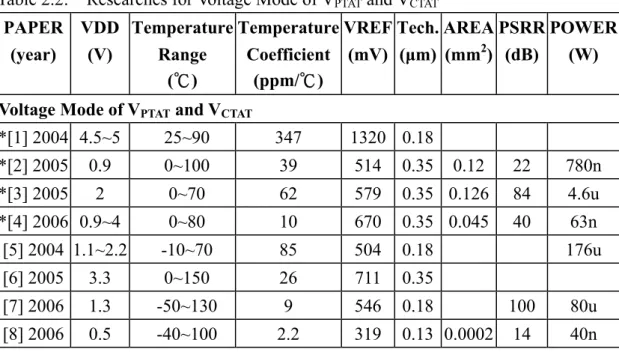
Those advantages are very powerful help for designing voltage reference in battery-operated system. In Table 2.2, it shows researches for voltage mode of VPTAT
and VCTAT. The power can scale down to several dozens nano-Amp and the area can
reach μm2. Under comparison, the performance certainly does not lose to bandgap reference.
Table 2.2: Researches for Voltage Mode of VPTAT and VCTAT
PAPER (year) VDD (V) Temperature Range (℃) Temperature Coefficient (ppm/℃) VREF (mV) Tech. (μm) AREA (mm2) PSRR (dB) POWER (W) Voltage Mode of VPTAT and VCTAT
*[1] 2004 4.5~5 25~90 347 1320 0.18 *[2] 2005 0.9 0~100 39 514 0.35 0.12 22 780n *[3] 2005 2 0~70 62 579 0.35 0.126 84 4.6u *[4] 2006 0.9~4 0~80 10 670 0.35 0.045 40 63n [5] 2004 1.1~2.2 -10~70 85 504 0.18 176u [6] 2005 3.3 0~150 26 711 0.35 [7] 2006 1.3 -50~130 9 546 0.18 100 80u [8] 2006 0.5 -40~100 2.2 319 0.13 0.0002 14 40n
2.3.2 Current Mode of V
PTATand V
CTATThe circuit refers to Ref [10]: A Simple Subthreshold CMOS Voltage Reference Circuit With Channel-Length Modulation Compensation. It is assorted to current mode of VPTAT and VCTAT. The circuit uses MOS works in subthreshold region to
produce a reference voltage of 221mV at supply voltage of 0.85V. The power consumption has only 3.3μW at room temperature uses TSMC 0.18μm technology. The area of proposed circuit is less than 0.0238 mm2, and the reference voltage variation is 2mV/V for supply voltage from 0.9 to 2.5V. Beside, the temperature variation is 6mV in the range from -20℃~120℃. (Ref: [10])
Figure 2.3.2: Circuit Architecture for Current Mode of VPTAT and VCTAT (REF[10]) The circuit is a typical current mode of VPTAT and VCTAT, and it is divided into
three parts.
1. CTAT part: It is made of transistors M1 to M5 and resistor R1. To analyze the circuit, M3 operates in subthreshold region. VGS3 is negative-temperature voltage.
So, we can know that (2-19).
C GS B R I V I = − 1 3 (2-19)
IC is used to compensate channel-length modulation. IB is a current of
negative-temperature coefficient, so ICTAT is produced in this part.
2. PTAT part: A general IPTAT generator is made of transistors M6 to M9 and
resistor R2. Transistors M8 and M9 operate in subthreshold region, and the function is as follows : (2-20)
(
)
2 2 9 8 R V R V V IA GS GS GS Δ = − = (2-20)ΔVGS is positive-temperature voltage, so IA is positive-temperature current. Therefore
IPTAT is produced in the part.
3. VREF part: Using transistors M10 to M11 and resistor R3, we can get VREF. The
function of VREF is as follows : (2-21)
( )
( )
( )
( )
3 2 11 7 10 * R I L W L W I L W L W VREF A B ⎟⎟ ⎟ ⎠ ⎞ ⎜⎜ ⎜ ⎝ ⎛ + = (2-21)Although, those circuit can be designed in low voltage architecture, but they always need resistors. It must cause big area, so it is not easy to accord with our goal which is design in battery-operated system. Besides, resistors have more variation in standard CMOS process. It may decrease the accuracy of voltage reference. Further, voltage reference is the currents to multiply the resistor. If VREF needs a higher value,
the currents and resistor must be large enough to reach the value. Therefore, power is hard to decrease.
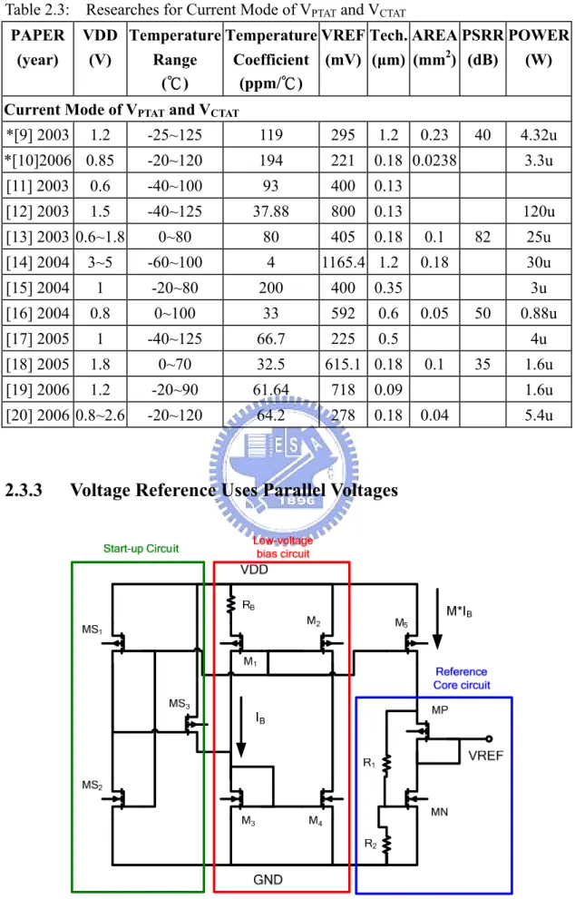
In Table 2.3, it shows researches for current mode of VPTAT and VCTAT. We can
discover that temperature coefficient of current mode is not better than voltage mode. Because current mode of VPTAT and VCTAT needs current mirror and resistors, they will
cause deviation of voltage reference. Therefore, temperature coefficient is difficult to scale down. The power is hard to scale down, too. Those issues have been illustrated in the above section.
Table 2.3: Researches for Current Mode of VPTAT and VCTAT PAPER (year) VDD (V) Temperature Range (℃) Temperature Coefficient (ppm/℃) VREF (mV) Tech. (μm) AREA (mm2) PSRR (dB) POWER (W) Current Mode of VPTAT and VCTAT
*[9] 2003 1.2 -25~125 119 295 1.2 0.23 40 4.32u *[10]2006 0.85 -20~120 194 221 0.18 0.0238 3.3u [11] 2003 0.6 -40~100 93 400 0.13 [12] 2003 1.5 -40~125 37.88 800 0.13 120u [13] 2003 0.6~1.8 0~80 80 405 0.18 0.1 82 25u [14] 2004 3~5 -60~100 4 1165.4 1.2 0.18 30u [15] 2004 1 -20~80 200 400 0.35 3u [16] 2004 0.8 0~100 33 592 0.6 0.05 50 0.88u [17] 2005 1 -40~125 66.7 225 0.5 4u [18] 2005 1.8 0~70 32.5 615.1 0.18 0.1 35 1.6u [19] 2006 1.2 -20~90 61.64 718 0.09 1.6u [20] 2006 0.8~2.6 -20~120 64.2 278 0.18 0.04 5.4u
2.3.3
Voltage Reference Uses Parallel Voltages
A voltage reference is necessary for LDO design, and it provides a low-supply-dependence and low-temperature-drift reference voltage to define the LDO output voltage. The circuit refers to Ref[21]: A CMOS Voltage Reference Based On Weighted △Vgs For CMOS Low-Dropout Linear Regulators. It is assorted to parallel voltages. A CMOS voltage reference been implemented in a standard 0.6μm CNOS technology. The area is 0.055mm2, and the lowest supply voltage is 1.4V. A typical temperature coefficient is 36.9 ppm/℃. (Ref: [21])
The proposed CMOS voltage reference is based on the different temperature dependencies of the threshold voltages of an NMOS and a PMOS. See Fig 2.3.3, it can be divided into three parts.
1. Start-up circuit: It is formed by MS1-MS3. It uses to trigger this circuit, when the circuit operates in wrong state.
2. Low-voltage bias circuit: It is formed by M1-M4 and RB. It provides a stable
bias current.
3. Reference core circuit: It is formed by M5, MP, MN, R1 and R2. Its function of
VREF is showed as follows: (2-22)
GSp GSn REF V V R R V ⎟⎟ − ⎠ ⎞ ⎜⎜ ⎝ ⎛ + = 2 1 1 (2-22)
Using two parallel voltages which mean two VGS to subtract is a method to
produce voltage reference. But, the architecture has two disadvantages. First, two slopes of VGS is not parallel, because the two MOS is not in the same situation which means different VBS and different MOS type. This will cause inexactitude voltage
reference. See Table 2.4, we discover temperature coefficient of the architecture is not bad, but they almost do not have good temperature range. Second, these circuits have a disadvantage which is resistors. Because we need most current (M*IB) run through
MP and MN, resistors R1 and R2 must be large enough. This causes the resistor
Table 2.4: Researches of Voltage Reference of Parallel Voltages PAPER (year) VDD (V) Temperature Range (℃) Temperature Coefficient (ppm/℃) VREF (mV) Tech. (μm) AREA (mm2) PSRR (dB) POWER (W) Voltage Reference Uses Parallel Voltages
*[21]2003 1.4 0~100 36.9 309 0.6 0.055 20 13.58u *[22]2004 5 -10~80 32 2670 0.5 0.0936 970u *[23]2005 1.5 0~80 25 168 0.35 0.08 59 3.6u *[24]2006 1.5~4.3 0~80 12 891.1 0.35 0.015 59 300n [25] 2005 0.6~1.8 0~75 70 332 0.18 [26] 2006 0.9~3.3 -40~100 33 181 0.35 1.1u
2.3.4
Zero Temperature Coefficient Point (ZTC)
The circuit refers to Ref[27]: Mutual Compensation of Mobility and Threshold Voltage Temperature Effects with Applications in CMOS Circuits. It is assorted to ZTC. Mutual compensation of mobility and threshold voltage temperature variations may result in a ZTC (zero temperature coefficient) bias point of a MOS transistor. The circuit can be applied in voltage reference circuits and temperature sensors with linear dependence of voltage versus temperature. (Ref: [27])
See Figure 2.3.4, Q1 operates on ZTC point. To use feedback to stabilize MOS Q1, so variations will decrease. In the circuit, for transistor Q1 the following design relationship should be satisfied
3 1 2 3 1 2 1 1 R R R V R R R V I ID = DF = GS = GSF (2-23)
The values of IDF = 192μA and VGSF = 869mV were considered as the parameters of
the ZTC bias point at T=T0=300°K.
But ZTC has a problem that VREF is hard to be designed in ultra low voltage.
That is because MOS has no ZTC point in ultra low voltage. In Table 2.5, VREF can’t
be lower than 600mV, even if supply voltage scales down 1V. Therefore, the architecture is hard to apply in battery-operated system.
Table 2.5: Researches of ZTC PAPER (year) VDD (V) Temperature Range (℃) Temperature Coefficient (ppm/℃) VREF (mV) Tech. (μm) AREA (mm2) PSRR (dB) POWER (W) ZTC *[27]2001 3~3.3 -20~100 15 799 0.35 0.0204 [28]2004 1 -50~150 4 640 0.18 [29]2005 3.3 -50~120 50 821 1264 0.35 36.3u
2.3.5 Voltage
Reference
Uses Non-standard Process
The circuit refers to Ref [30]: CMOS Voltage Reference Based on Gate Work Function Differences in Poly-Si Controlled by Conductivity Type and Impurity Concentration. It is assorted to special process. A new CMOS reference circuit consisting of two pairs of transistors is presented. One pair exhibits a threshold voltage difference with a negative temperature coefficient, while the other exhibits a positive temperature coefficient. (Ref: [30])
Figure 2.3.5: Circuit Architecture of Non-standard Process (REF[30])
For a pair of MOS transistors with gates of different conductivity types or different impurity concentrations, it will produce VPTAT or VCTAT, see Figure 2.3.6.
Vpn(V ) Vnn(V) 0 0.005 0.01 0.015 0.02 0.025 0.03 ‐50 ‐40 ‐30 ‐20 ‐10 0 10 20 30 40 50 60 70 80 90 100 1.12 1.13 1.14 1.15 1.16 1.17 1.18 1.19 1.2 1.21 ‐50 ‐40 ‐30 ‐20 ‐10 0 10 20 30 40 50 60 70 80 90 100
Figure 2.3.6: (a) Vpn and (b) Vnn as a Function of Temperature In Figure 2.3.5, we can know
pn V R R R V R R R 2 1 2 1 2 1 2 2 V + = + = . (2-24)
pn nn V R R R 2 1 2 REF V V + + = (2-25)
We just adjust R1 and R2, so VREF can be designed very well.
Although, special process needs not only standard CMOS process technique, so it may want to have special or additional process. This will cause more cost and resource, but we don’t hope to see. In Table 2.6, it is researches of Non-standard Process. Some researches use floating-gate to design voltage reference, and it is also Non-standard Process.
Table 2.6: Researches of Voltage Reference of Non-standard Process
PAPER (year) VDD (V) Temperature Range (℃) Temperature Coefficient (ppm/℃) VREF (mV) Tech. (μm) AREA (mm2) PSRR (dB) POWER (W) Voltage Reference Uses Non-standard Process
*[30]2003 1 -50~100 80 410 0.6u
*[31]2004 2.8~5.5 -20~100 54.6 0.8~1.5 0.5 0.081 80 500u *[32]2005 4.5~9 -40~85 1 1250~5000 1.5 1.6 67 3.15u *[33]2006 1.2 -60~140 130 400 0.35 0.0022 40u
2.3.6
Comparison of Voltage Reference
See Table 2.7, it is comparison of the above five circuit architectures. Our goal is to design voltage reference in battery-operated systems which demand low-power and small-area. Because there is no ZTC in ultra low voltage, ZTC architecture does not match with our goal. On the other hand, current mode of PTAT and CTAT architecture and parallel voltages architecture always need resistances which occupy the bigger area and cause more derivation, so they do not match our goal, too. Special process always needs additional process steps which will increase cost that we do not want to see.
Table 2.7: Comparison for Five Kinds of CMOS Voltage References
Comparison
Voltage Mode of VPTAT and VCTAT 1. Can no resistor
2. Power arrives to nano-Watt Current Mode of VPTAT and VCTAT 1. Resistor and current trade off Voltage Reference Uses Parallel Voltages 1. Need resistors
ZTC 1. No ZTC in ultra low voltage Voltage Reference Uses Non-standard
Process
1. No apply in standard process
See Table 2.8, it is researches for CMOS voltage reference, and five circuit architectures has been assorted. We can discover that performance of voltage mode is better than performance of other architectures. First, temperature coefficient is low generally at voltage mode of VPTAT and VCTAT, and temperature range is wide enough.
Second, power of voltage mode of VPTAT and VCTAT can scale down to several dozens
nW. It is very beneficial to design voltage reference in battery-operated system. Third, small area is achieved at voltage mode of VPTAT and VCTAT. We can see that area is
several hundred μm2, and no other architectures are batter than voltage mode of V PTAT
and VCTAT. Although, special process has the same small area, it needs additional
process steps which will increase costs. Therefore, we don’t consider special process.
Table 2.8: Researches for All CMOS Voltage Reference
PAPER (year) VDD (V) Temperature Range (℃) Temperature Coefficient (ppm/℃) VREF (mV) Tech. (μm) AREA (mm2) PSRR (dB) POWER (W) Voltage Mode of VPTAT and VCTAT * is that research has experimental result
*[1]2004 4.5~5 25~90 347 1320 0.18 *[2]2005 0.9 0~100 39 514 0.35 0.12 22 780n *[3]2005 2 0~70 62 579 0.35 0.126 84 4.6u *[4]2006 0.9~4 0~80 10 670 0.35 0.045 40 63n [5] 2004 1.1~2.2 -10~70 85 504 0.18 176u [6] 2005 3.3 0~150 26 711 0.35 [7] 2006 1.3 -50~130 9 546 0.18 100 80u [8] 2006 0.5 -40~100 2.2 319 0.13 0.0002 14 40n
Current Mode of VPTAT and VCTAT *[9]2003 1.2 -25~125 119 295 1.2 0.23 40 4.32u *[10]2006 0.85 -20~120 194 221 0.18 0.0238 3.3u [11] 2003 0.6 -40~100 93 400 0.13 [12] 2003 1.5 -40~125 37.88 800 0.13 120u [13] 2003 0.6~1.8 0~80 80 405 0.18 0.1 82 25u [14] 2004 3~5 -60~100 4 1165.4 1.2 0.18 30u [15] 2004 1 -20~80 200 400 0.35 3u [16] 2004 0.8 0~100 33 592 0.6 0.05 50 0.88u [17] 2005 1 -40~125 66.7 225 0.5 4u [18] 2005 1.8 0~70 32.5 615.1 0.18 0.1 35 1.6u [19] 2006 1.2 -20~90 61.64 718 0.09 1.6u [20] 2006 0.8~2.6 -20~120 64.2 278 0.18 0.04 5.4u
Voltage Reference Uses Parallel Voltages
*[21]2003 1.4 0~100 36.9 309 0.6 0.055 20 13.58u *[22]2004 5 -10~80 32 2670 0.5 0.0936 970u *[23]2005 1.5 0~80 25 168 0.35 0.08 59 3.6u *[24]2006 1.5~4.3 0~80 12 891.1 0.35 0.015 59 300n [25] 2005 0.6~1.8 0~75 70 332 0.18 [26] 2006 0.9~3.3 -40~100 33 181 0.35 1.1u ZTC *[27]2001 3~3.3 -20~100 15 799 0.35 0.0204 [28] 2004 1 -50~150 4 640 0.18 [29] 2005 3.3 -50~120 50 821 1264 0.35 36.3u
Voltage Reference Uses Non-standard Process
*[30]2003 1 -50~100 80 410 0.6u
*[31]2004 2.8~5.5 -20~100 54.6 0.8~1.5 0.5 0.081 80 500u *[32]2005 4.5~9 -40~85 1 1250~5000 1.5 1.6 67 3.15u *[33]2006 1.2 -60~140 130 400 0.35 0.0022 40u
In researches for voltage mode of VPTAT and VCTAT, Ref [2] is good to discuss in
depth, because it has several characteristics.
1. Low power: In researches for voltage mode of VPTAT and VCTAT, Ref[2] is sole
circuit architecture at which all MOS work in subthreshold region. It is very worth to investigate in depth, because MOS work in subthreshold region can reach the least power consumption.
2. Small area: The area of circuit architecture which is Ref[2] is (400*300)μm2, and we find that resistors occupy a lot of area. Therefore, we try to delete the resistors, and we will save very big area to reach the goal of small area.
3. Simple: Circuit architectures will demand simple and high performance in the future. Simple doesn’t produce needless performance which effect accuracy, and simple circuit can decrease power consumption.
Choosing voltage mode of VPTAT and VCTAT architecture as our design
architecture is possible to implement our goal. Because of no resistances, the area can diminish largely and decrease resistor’s error. Besides, MOS which works in subthreshold region is adaptable to design in low-power architectures.
2.3.7
Summary
In this chapter, we know that voltage references are produced by VPTAT and VCTAT.
Introducing bandgap references, and comparing BJT and MOS. Making sure that MOS is better than BJT under our requests. Afterward we introduce five architectures of voltage references and understand how they work. Finally, comparison is shown in the last section. After comparison, we choose voltage mode of VPTAT and VCTAT as our
design architecture.
In the next chapter, two propose design architectures will be shown carefully. We will introduce principle, derivation, and simulation gradually, and my propose architectures compare with researches which is presented in the recent six years.
CHAPTER
3
Circuitry Architecture
In this chapter, proposed architectures will be shown and implemented. Before this, we should define specification explicitly. At least, proposed design can work in battery-operated system, and it still has high performance. Then, we start to find out VCTAT which must be produced by MOS, and using VCTAT produces VPTAT if it could
be implemented. When having VCTAT and VPTAT, we can design voltage reference
stage by stage. Two proposed architectures will be shown and simulated, and we discuss their advantages and problems. Finally, two proposed architectures compare to researches, and explain that proposed architectures are better then researches in the recent six years.
3.1 Design Process
First, we introduce two papers, and those are source of my proposed architectures. So we need to understand the two reference papers step by step. Then we will be clear to know how proposed architectures are designed.
3.1.1 Reference Paper
In Figure 3.1.1, all MOS work in subthreshold region, so VGS is VCTAT. See M8, VG8 is
VDD and VGS8 is VCTAT, so we can know that VS8 will be VPTAT. But the current which
pass through M7 and M8 changes VGS8 by the current function, so VS8 becomes VREF.
We can design the bias circuit which produces VPTAT by this principle. In next section,
CTAT DD
PTAT V V
V = − (3-1)
Figure 3.1.1: Circuit Architecture of REF[8]
.1.2 V
PTAT(Proportional to Absolute Temperature)
3
VDD GND R M3 M4 M1 M2 VPTAT IPTAT I2The conve circu
ntional method which produces VPTAT is shown Figure 3.1.2. The
it composes of four MOS (M1~M4) and a resistor (R). M1 and M2 work in subthreshold region, and M3 and M4 work in saturation region. R is stable value which doesn’t change with temperature. The derivation is as follows:
Because M1 and M2 work in subthreshold region, the function is (3-2)
⎟ ⎟ ⎟ ⎟ ⎠ ⎞ ⎜ ⎜ ⎜ ⎜ ⎝ ⎛ ⎟ ⎠ ⎞ ⎜ ⎝ ⎛ + = L W I T I q kT n T V T V S DS th GS ) ( ln ) ( ) ( (3-2) ,and (3-3) Using (3-2) into (3-3) can be shown as follows:
PTAT GS GS V V V 1 = 2+ PTAT S DS TH S DS TH V L W I T I q kT n T V L W I T I q kT n T V + ⎥ ⎥ ⎥ ⎥ ⎦ ⎤ ⎢ ⎢ ⎢ ⎢ ⎣ ⎡ ⎤ ⎡ ⎟ ⎠ ⎞ ⎜ ⎝ ⎛ + = ⎥ ⎥ ⎥ ⎥ ⎦ ⎢ ⎢ ⎢ ⎢ ⎣ ⎟⎠ ⎞ ⎜ ⎝ ⎛ + 2 2 1 1( ) ( ) ln ( ) ln ) ( (3-4)
,then we get the function of (3-5)
⎥ ⎥ ⎥ ⎥ ⎦ ⎤ ⎡ ⎟ ⎞ ⎜ ⎛W ⎢ ⎢ ⎢ ⎢ ⎣ ⎟⎠ ⎞ ⎜ ⎝ ⎛ ⎠ ⎝ = 1 2 2 1 ln L W L I I q kT n V DS DS PTAT (3-5) , so 4 3 2 1: DS DS : DS DS I I I I = 4 3 2 1 : : ⎟ ⎠ ⎞ ⎜ ⎝ ⎛ ⎟ ⎠ ⎞ ⎜ ⎝ ⎛ = ⎟ ⎠ ⎞ ⎜ ⎝ ⎛ ⎟ ⎠ ⎞ ⎜ ⎝ ⎛ L W L W L W L W
⎥ ⎥ ⎥ ⎥ ⎦ ⎤ ⎢ ⎢ ⎢ ⎢ ⎣ ⎡ ⎟ ⎠ ⎞ ⎜ ⎝ ⎛ ⎟ ⎠ ⎞ ⎜ ⎝ ⎛ ⎟ ⎠ ⎞ ⎜ ⎝ ⎛ ⎟ ⎠ ⎞ ⎜ ⎝ ⎛ = 1 2 4 3 ln L W L W L W L W q kT n VPTAT (3-6) Because ⎥ ⎥ ⎥ ⎥ ⎦ ⎤ ⎢ ⎢ ⎢ ⎢ ⎣ ⎡ ⎟ ⎠ ⎞ ⎜ ⎝ ⎛ ⎟ ⎠ ⎞ ⎜ ⎝ ⎛ ⎟ ⎠ ⎞ ⎜ ⎝ ⎛ ⎟ ⎠ ⎞ ⎜ ⎝ ⎛ 1 2 4 3 ln L W L W L W L W
is a positive value, VPTAT is in positive proportion to
temperature. And VPTAT=I2*R, we can know that I2=IPTAT. Therefore, we get VPTAT and
IPTAT.
Although, the circuit is better than bandgap reference. But, it has some disadvantages. First, supply voltage is difficult below 1V. The minimum VDD =
VGS4(saturation) + VGS1(subthreshold) + VPTAT, and VGS4 > VTH, VGS1 < VTH, VPTAT
should have a value. VTH is about 0.45V at TSMC 0.18μm process. Therefore, we can
know that supply voltage will be more 1V. Second, resistor must be used, and it will cause additional inaccuracy and more area. Because VPTAT must reach a fixed value,
the R and IPTAT should large enough. It means that area and power must choose one. In
addition, someone change resistor to MOS which work in triode region as a resistor. Indeed, the method could decrease a lot of area. But the method needs additional circuits, the power is possible to increase. So, I propose a simple circuit to solve those problems. I will explain proposed circuit of VPTAT in the next section.
Figure 3.1.3: The VPTAT Proposed Architecture
See Figure 3.1.3, it is proposed circuit of VPTAT. The circuit is composed of three
NMOS (M1~M3). All MOS work in subthreshold region, so VGS is VCTAT which is a
voltage of negative temperature coefficient. And, VDD is a stable value. Therefore,
VPTAT is as follows: 3 1 DD CTAT DD GS GS PTAT V V V V V V = = − = − (3-7)
VPTAT is gotten by two MOS which work in subthreshold region. The supply voltage
In the next section, the two proposed circuit of voltage reference is shown. We of proposed circuit can be lower than 1V because it stacks two MOS which are about 0.8V. And, the area of proposed circuit is very small because it has only two MOS. So, the proposed circuit could have advantages of both small area and low supply voltage.
will discuss principle, derivation, simulation, and problem. The relationship of proposed architectures will be illustrated.
3.2 All NMOSFET Voltage Reference (ANVR)
ture can be shown. Its a
When we present new bias-circuit, the first proposed architec
bbreviation is ANVR which means All NMOSFET Voltage Reference. The proposed architecture will introduce principle, derivation, and simulation in the next section.
Figure 3.2.1: Architecture of ANVR
M1 M2 M3 M4 R(ohm) W( 4.976k μm) 0.5 0.5 0.9 0.9 L(μm) 0.6 0.6 0.6 0.6 m 6 6 6 6
.2.1 Principle
of
ANVR
See Figure 3.2.1, the proposed architecture is composed of four NMOS (M1~M4)
3
and one resistor. All MOS work in subthreshold region. M1 and M3 are VPTAT
produced circuit which has been introduced in the above section, and it produces a stable VPTAT to mirror to next stage. M2 and M4 are VREF produced circuit. We use
off. By this, a stable VREF will be produced. Because we hope that ANVR can operate
under 1V, we choose VTH of MOS around 0.48V. Besides, we hope that proposed
architecture’s power can be lower than the power of PAPER [2]. Therefore, we decide that supply voltage is 0.8V and total current is about 500nA. The each current of ANVR is 250nA which is the same current at the architecture of PAPER [2]. Finally, we can know the size of MOS and the derivation can be shown in the next section.
3.2.2
Derivation of ANVR
The section will derivate VREF and illustrate every parameters. First, bias-circuit
deriv
. Bias-circuit derivation
1 is shown as
(3-8) Using the current function of MOS works in weak inversion, the function of (3-8) can be written as
ation is shown, and VREF-circuit derivation will be shown by bias-circuit
derivation later. Therefore we can decide (W/L) and resistor by the derivation.
A
First, the function of VGS
( )
T V V( )
T VGS1 = DD − GS3( )
( )
( )
( )
( )
⎭ ⎬ ⎫ ⎩ ⎨ ⎧ − + ⎥ ⎦ ⎤ ⎢ ⎣ ⎡ + − = ⎭ ⎬ ⎫ ⎩ ⎨ ⎧ ⎥ ⎦ ⎤ ⎢ ⎣ ⎡ + − = T V T V P P nV T V V P I T I nV T V V V th GS T th DD S D T th DD GS 1 1 3 1 3 3 3 3 1 ln ln (3-9)P is (W/L), VT is thermal voltage, and n is subthreshold slope factor. The function
of (3-9) become as
( )
[
V( )
T V( )
T]
P P nV V T VGS DD T th1 th3 3 1 1 2 1 ln 2 1 2 1 − − ⎥ ⎦ ⎤ ⎢ ⎣ ⎡ − = (3-10)B.
(3-11) Using the current function of MO
can be written as
VREF-circuit derivation
REF can be written as the function
V
( )
( )
[
V T I T R]
V
VREF = DD − GS4 + D2 ×
S works in weak inversion, the function of (3-11)
( )
( )
( )
( )
( )
( )
( )
( )
( )
( )
( )
⎥ ⎦ ⎤ ⎢ ⎣ ⎡ − + × + + ⎥ ⎦ ⎤ ⎢ ⎣ ⎡ − = ⎥ ⎥ ⎥ ⎥ ⎥ ⎦ ⎤ ⎢ ⎢ ⎢ ⎢ ⎢ ⎣ ⎡ × + ⎥ ⎥ ⎥ ⎥ ⎥ ⎦ ⎤ ⎢ ⎢ ⎢ ⎢ ⎢ ⎣ ⎡ ⎥ ⎦ ⎤ ⎢ ⎣ ⎡ − + − = ⎥ ⎦ ⎤ ⎢ ⎣ ⎡ × + ⎤ ⎡ + − =V V I T V D th DD REF 2 4 ⎥ ⎦ ⎢ ⎣ T V T V R T I T V P P nV V R T I P I nV T V T V P I nV T V V R T I P I nV T th th D GS T DD D S T th GS S T th DD D S T 2 4 2 2 4 2 2 4 2 2 2 4 2 4 ln exp ln ln (3-12)the function of (3-12) can become as (3-13) by the function of (3-10)
( )
( )
[
]
( )
( )
( )
( )
T R V( )
T V( )
T V( )
T V( )
T I P P nV P P nV V T V T V R T I T V T V P nV V P nV V VREF DD T DD T th1 th3 D2 3 4 2 ln 2 2 ln ⎢ ⎢ ⎣ ⎢⎣ ⎦⎥+⎩⎨ − ⎢⎣ ⎥⎦− − ⎬⎭+ − = P P th th th th D T T DD th th 2 4 3 1 2 3 1 4 2 2 4 1 2 2 1 2 1 ln 2 1 ln 2 1 1 1 1 + − − + × − ⎥ ⎦ ⎤ ⎢ ⎣ ⎡ + ⎥ ⎦ ⎤ ⎢ ⎣ ⎡ − = ⎥ ⎥ ⎦ ⎤ ⎡ − + × ⎫ ⎧ ⎡ ⎤ ⎤ ⎡ (3-13) If we want VREF which does not change with temperature, dVREF/dT should bezero.
( )
( )
( )
( )
( )
0 2 ln 2 1 3 2 4 3 1 2 4 = ⎥⎦ ⎤ ⎢⎣ − + ⎥⎦ ⎢⎣ − + − ⎪⎭ ⎬ ⎪⎩ ⎨ ⎥ ⎦ ⎢ ⎣ × ⎥ ⎦ ⎢ ⎣ = dT T dT dT dT dT R P P q n D th th th th (3-14) n is subthreshold slope factor , P is (W/L), and1 2 1 ⎡ ⎤ ⎡ ⎪⎫ ⎪⎧⎡P ⎤ ⎡P ⎤ dI T dV T dV T dV T dV k dT dVREF K ev q k =8.6×10⁻⁵ . The function of VTH(T) is shown as
( )
( ) (
)
⎟⎟ ⎠ ⎞ ⎜⎜ ⎝ ⎛ − × + + =V T0 KT1 T Vth th 2 1 0 T T V KT bs (3-15)And its differentiation is written as
( ) (
KT KT Vbs)
dT = 1+ 2× ( th T dV 3-16) KT1 is temperature coeffcoefficient of the threshold volta TH
decided when (W/L) had been decided. Therefore, dVREF(T)/dT can be zero by
desig
upply voltage is 0.8V which reaches below 1V. The circuit has only two NMOS to stack, and MOS work in subth
Simulation of ANVR
The layout of ANVR is shown in Figure 3.2.3. ANVR uses no PMOS, so the decrease area. M1 and M2 are lternate permutation, so it can decrease mismatch. IPTAT will mirror to M2 very well.
Beca
and all corners are shown in Table 3.4. Those gures are curve of VREF and temperature, and temperature range is wide enough to
icient of the threshold voltage and KT2 is bulk-bias ge’s temperature dependence. dV (T)/dT can been ning P1~P4. When we decide the power, the current will be decided. Then, (W/L)
is decided by the current. Finally, resistor can be chosen.
ANVR has many advantages. First, all MOS are NMOS. This method saves a lot area, because we don’t use the area of PMOS. Second, s
reshold region which means VTH < 0.45V. Therefore, we can decrease much
power in the proposed architecture. Third, the performance is not bad, and it will be shown in next section.
3.2.3
Post-Layout
layout does not need PMOS region. It is good to a
use a resistor has larger derivation, we divide a resistor into eight resistors. The method can decrease resistor derivation. In addition, dummy technique has been used in the layout, and it is also used to decrease process variation. Figure 3.2.2 shows presim of ANVR, and we can compare with Figure 3.2.3 which shows postsim of ANVR. They are almost the same.
The post-layout simulation is shown in Table 3.3. The five corners are shown from Figure 3.2.4 to Figure 3.2.8,
reach -80℃~165℃. The inaccuracy is only ±1.5mV at Figure 3.2.3 when the corner is TT and TT_RES. In Table 3.3, temperature coefficient is lower than 166ppm/℃ in the worst case when temperature range is -80℃~165℃. We try to adjust the corners of proposed architecture, so temperature coefficient of the worst case can lower than 200 ppm/℃.
Temperature VS.Vref (TSMC 0.18um CMOS technology)
-100 -50 0 50 100 150 200 354.5 355 355.5 356 356.5 357 357.5 358 Temperature=-80 to 165 DEC-C Vr e f(T ) m v 356.25mV
Figure 3.2.2: Presim of ANVR
Table 3.1: Post-Layout S PAPER (year) VDD (V) Temperature Range Temperature Coefficient VREF (mV) Tech. (μm) AREA (mm2) PSRR (dB) POWER (W) imulation of ANVR (℃) (ppm/℃) ANVR (TT S) -40~125 0~100 356.7 (3 2 @100kHz 403.2n ,TT_RE 0.8 -80~165 34.4 27.7 16.7 356 356.7 0.18 0.00108 0*36)μm 7.5
Figure 3.2.3: Layout of ANVR in TSMC 0.18um CMOS Technique
A. Post-Layout Simulation Results (VREF):
-100 -50 0 50 100 150 200 354.5 355 355.5 356 356.5 357 357.5 Temperature=-80 to 165 DEC-C V re f(T ) m v
Temperature VS.Vref (TSMC 0.18um CMOS technology)
356mV
354.5mV
357.5mV
-100 -50 0 50 100 150 200 344 346 348 350 352 354 356 Temperature=-80 to 165 DEC-C Vref (T ) m v
Temperature VS.Vref (TSMC 0.18um CMOS technology)
349.75mV
344mV 355.5mV
Figure 3.2.5: FF TT_RES Corner of ANVR
-100 -50 0 50 100 150 200 354 355 356 357 358 359 360 361 Temperature=-80 to 165 DEC-C Vref (T ) m v
Temperature VS.Vref (TSMC 0.18um CMOS technology)
357.15mV
354.2mV
360.1mV
-100 -50 0 50 100 150 200 355 356 357 358 359 360 361 Temperature=-80 to 165 DEC-C Vref (T ) m v
Temperature VS.Vref (TSMC 0.18um CMOS technology)
357.75mV
355.1mV
360.4mV
Figure 3.2.7: SF TT_RES Corner of ANVR
-100 -50 0 50 100 150 200 346 347 348 349 350 351 352 353 354 355 Temperature=-80 to 165 DEC-C Vre f(T ) m v
Temperature VS.Vref (TSMC 0.18um CMOS technology)
354.8mV
346mV 350.4mV
B. Post-Layout Simulation Results (VREF):
Table 3.2: Corners of ANVR Post-Layout Simulation (VREF)
Corner Resistance Corner Temperature Coefficient (ppm/℃) (0℃~100℃) Temperature Coefficient (ppm/℃) (-40℃~125℃) Temperature Coefficient (ppm/℃) (-75℃~165℃) Temperature Coefficient (ppm/℃) (-80℃~165℃) TT TT 16.7(0.6) 28(1.65) 32.7(2.8) 34.4(3) FF 23.7(0.85) 33.1(1.95) 36.8(3.15) 38.4(3.35) SS 22.4(0.8) 30.6(1.8) 37(3.2) 36.7(3.2) FF TT 153.1(5.4) 137.9(8) 137(11.5) 134.2(11.5) FF 113.5(4) 103.4(6) 103.7(8.7) 101.1(8.7) SS 193.5(6.5) 169.5(9.8) 170.5(14.1) 165.3(14.1) SS TT 72.5(2.5) 72.8(4.3) 66.4(5.6) 67.4(6) FF 75.3(2.8) 76.2(4.5) 50.1(6.1) 73.1(6.4) SS 64.2(2.4) 67.8(4) 63(5) 61.8(5.4) SF TT 64(2.2) 64.2(3.8) 59.3(5) 60.5(5.3) FF 69.5(2.5) 71(4.2) 66.3(5.6) 67.3(5.9) SS 55.7(2) 57.5(3.4) 54.7(4.6) 56(4.9) FS TT 167.7(4) 103.4(6) 103.4(8.8) 102.5(8.8) FF 79.1(2.9) 73.8(4.3) 76.9(6.6) 76.6(6.6) SS 141.8(10.9) 131.3(7.6) 132.5(11.1) 129.8(11.1)
( ) is derivation of voltage reference, and its unit is mV.
3.2.4
Discussion of ANVR
The performance of proposed architecture is good, but PSRR is lower than the most researches. VREF will shake easily when supply voltage shakes. And ANVR has
used resistors which have a derivation. Besides, the circuit needs to have a stable mechanism which can stabilize bias circuit. The three issues deserve to discuss, and we need to find solutions. In the next section, NPVR is presented to solve the above issues.
3.3
NMOSFET and PMOSFET Voltage Reference
(NPVR)
When we advance problem from ANVR, the second proposed architecture can be shown to solve the problem. Its abbreviation is NPVR which means 3.3
NMOSFET and PMOSFET Voltage Reference. The proposed architecture will introduce principle, derivation, and simulation in the next section.
Figure 3.3.1: Architecture of NPVR M1 M2 M3 M4 M5 M6 M7 M8 W(μm) 1 1 1 1 1 1 0.5 0.92 L(μm) 0.2 0.2 0.2 0.2 0.2 0.2 0.2 0.2 m 8 8 8 8 16 16 8 8
3.3.1
Principle of NPVR
The circuit is composed of NMOS and PMOS. M1~M4, M7, and M8 are NMOS, and M5~M6 are PMOS. All MOS work in subthreshold region. The principle is like


![Figure 2.3.1: Circuit Architecture for Voltage Mode of V PTAT and V CTAT (REF[2])](https://thumb-ap.123doks.com/thumbv2/9libinfo/8496662.184978/22.892.235.655.362.767/figure-circuit-architecture-voltage-mode-ptat-ctat-ref.webp)
![Figure 2.3.2: Circuit Architecture for Current Mode of VPTAT and VCTAT (REF[10]) The circuit is a typical current mode of V PTAT and V CTAT , and it is divided into three parts](https://thumb-ap.123doks.com/thumbv2/9libinfo/8496662.184978/25.892.152.747.419.823/figure-circuit-architecture-current-circuit-typical-current-divided.webp)
![Figure 2.3.4: Circuit Architecture of ZTC (REF[26])](https://thumb-ap.123doks.com/thumbv2/9libinfo/8496662.184978/29.892.222.692.626.1108/figure-circuit-architecture-of-ztc-ref.webp)
![Table 2.5: Researches of ZTC PAPER (year) VDD (V) Temperature Range (℃) TemperatureCoefficient(ppm/℃) VREF(mV) Tech.(μm) AREA (mm2) PSRR (dB) POWER(W) ZTC *[27]2001 3~3.3 -20~100 15 799 0.35 0.0204 [28]2004 1 -50~150 4 640 0.18 [2](https://thumb-ap.123doks.com/thumbv2/9libinfo/8496662.184978/30.892.129.766.523.768/table-researches-paper-temperature-range-temperaturecoefficient-psrr-power.webp)

