Low voltage lead titanate/Si one-transistor ferroelectric memory with good device
characteristics
C. L. Sun, S. Y. Chen, C. C. Liao, and Albert Chin
Citation: Applied Physics Letters 85, 4726 (2004); doi: 10.1063/1.1814440 View online: http://dx.doi.org/10.1063/1.1814440
View Table of Contents: http://scitation.aip.org/content/aip/journal/apl/85/20?ver=pdfcov Published by the AIP Publishing
Articles you may be interested in
Resistive switching characteristics in dielectric/ferroelectric composite devices improved by post-thermal annealing at relatively low temperature
Appl. Phys. Lett. 104, 092903 (2014); 10.1063/1.4867260
Retention in nonvolatile silicon transistors with an organic ferroelectric gate Appl. Phys. Lett. 94, 263507 (2009); 10.1063/1.3158959
Semiconductive metal oxide ferroelectric memory transistor: A long-retention nonvolatile memory transistor Appl. Phys. Lett. 86, 123513 (2005); 10.1063/1.1886252
Low-temperature integration of lead-based ferroelectric capacitors on Si with diffusion barrier layer Appl. Phys. Lett. 80, 3599 (2002); 10.1063/1.1477281
Fabrication and characterization of a Pb 5 Ge 3 O 11 one-transistor-memory device Appl. Phys. Lett. 79, 1661 (2001); 10.1063/1.1401092
This article is copyrighted as indicated in the article. Reuse of AIP content is subject to the terms at: http://scitation.aip.org/termsconditions. Downloaded to IP: 140.113.38.11 On: Thu, 01 May 2014 04:06:30
Low voltage lead titanate/Si one-transistor ferroelectric memory with good
device characteristics
C. L. Suna) and S. Y. Chen
Department of Materials Science and Engineering, National Chiao Tung University, Hsinchu, Taiwan, Republic of China
C. C. Liao and Albert Chin
Department of Electronics Engineering, National Chiao Tung University, Hsinchu, Taiwan, Republic of China
(Received 30 April 2004; accepted 1 September 2004)
We have developed one-transistor ferroelectric memory using lead titanate(PTO) as a gate dielectric directly formed on Si without any buffer layer. The PTO/Si metal–oxide–semiconductor field-effect transistor memory has shown a large threshold voltage shift of 1.6 V at only ±4 V program/erase voltages. The corresponding good interface was achieved by lowering the anneal temperature to 450 °C. Besides the sharp capacitance change of 0.17F / V cm2, it was also evidenced by the high
mobility of 169 cm2/ V s close to high-HfO
2. In addition, long retention⬎1000 s and endurance
⬎1011 stress cycles in the device suggested good memory characteristics. © 2004 American
Institute of Physics. [DOI: 10.1063/1.1814440]
Among various memory devices, ferroelectric memories are particularly remarkable due to the unique nonvolatile be-havior, good scale down potential, and fast switching time. Currently, high capacity共⬎1 Mbyte兲 ferroelectric RAM has been demonstrated in the cell configuration consisting of one-transistor(1T) and one-capacitor. But in order to further scale down the cell size, it is necessary to integrate the ferro-electric materials in the 1T ferroferro-electric metal–oxide– semiconductor field-effect transistor(FeMOSFET).1–9 How-ever, the strong interface reaction between ferroelectric materials and Si remained the major technology obstacle for this 1T memory in the last decade.3Recently, the adoption of a buffer gate dielectric between ferroelectric materials and Si shed a light to overcome the interdiffusion problem as a re-sult of the inevitable high anneal temperature of ferroelectrics.4–8 For example, using Al2O3 as the good
di-electric and diffusion barrier,10,11 we have achieved the record large ferroelectric memory window of 13 V in this kind of stack gate structure.8 Unfortunately, the relatively large writing voltage was usually required owing to the volt-age drop on the Al2O3 dielectric so as to hinder the widely
industrial applications. On the other hand, although the low temperature process has already been demonstrated in the organic permanent memory transistor, it still requires rela-tively high operation voltage caused by thick gate insulator.9 Besides the good threshold voltage shift共⌬VT兲 at a low
writ-ing voltage, the high carrier mobility is also requested in mainstream MOSFET technology.12 Therefore, it is really challenging to develop a next-generation low voltage 1T Fe-MOSFET memory.
It has been reported that Pb共Zr,Ti兲O3solid solution with
higher Ti fraction would need a lower anneal temperature. Supposedly, this low anneal temperature should be helpful to prevent the formation of interfacial layer,13which is essential to decrease the programming voltage in the low voltage op-eration. To study this effect, we have calculated the electric field共Eferro兲 in the ferroelectric material:
Eferro= Vg/
冉
dferro+ferro
interface
dinterface
冊
. 共1兲The Eferro, ferro, and dferro are the electric field, dielectric
constant, and thickness in ferroelectric layer, where the
interfaceand dinterfaceare the dielectric constant, and thickness
in interfacial layer. Because the ⌬VT is from ferroelectric
polarization, a larger Eferro is desired. Thus, decreased
dinterface and ferro are the solution to increase the desired
Eferro. This can be also obtained by lowering the anneal tem-perature of lead titanate (PTO) simultaneously though the ferroelectric property of PTO may be degraded by trading off the Eferro. Thus in this letter we investigated lead titanate as a
ferroelectric gate material directly grown on Si substrates with the low temperature annealing. Particularly, while the anneal temperature could be lowered down to 450 °C, it in-dicates the potential application for embedded memories and could also help terminate the contamination to integrated cir-cuit.
P-type 4 in. Si wafers with a resistivity of approximately 10⍀ cm were used in this study. After device isolation and source–drain n+ region definition, the around 90-nm-thick PTO layer was deposited by spin coating, dried at 90 °C for 30 s, and annealed at 450 °C. The entire process details were
a)Electronic mail: [email protected] FIG. 1. 1 MHz C–V characteristics of PTO/Si FeMOS capacitor. The ca-pacitor size is 10−4cm2and the gate length of the FeMOSFET is 10µm.
APPLIED PHYSICS LETTERS VOLUME 85, NUMBER 20 15 NOVEMBER 2004
0003-6951/2004/85(20)/4726/3/$22.00 4726 © 2004 American Institute of Physics
This article is copyrighted as indicated in the article. Reuse of AIP content is subject to the terms at: http://scitation.aip.org/termsconditions. Downloaded to IP: 140.113.38.11 On: Thu, 01 May 2014 04:06:30
described in our previous reports.5–7 HF-vapor passivation10,11was used to suppress the native oxide forma-tion before PTO formaforma-tion. Finally, Al electrodes were formed and the device size was 10m⫻100m. The de-vice performance was characterized by capacitance–voltage
共C–V兲 and current–voltage 共I–V兲 measurements.
Figures 1 and 2 show the device memory characteristics measured from 1MHz C–V of FeMOS capacitor and drain current–gate bias voltage共ID–VG兲 characteristics of
FeMOS-FET, respectively. The very high IDin Fig. 2 is due to
high- property of PTO that is important for VLSI scaling down.10–13 The ferroelectric characteristics are evidenced from the clockwise C–V hysteresis loops and counterclock-wise ID–VGhysteresis loops, as shown by arrows. For a low
±4 V program and erase voltage, a memory window of 1.6 V is obtained from both the flatband voltage shift in C–V curves. Additionally, the⌬VT change in ID–VG
characteris-tics indicates the excellent memory device performance. The possible reason for such low writing voltage is because the gate voltage is directly applied on the ferroelectric material instead of generating the voltage drop on the interfacial layer or inserted dielectric diffusion barrier.8 Although the PTO annealed at low temperature could have a relatively poor crystallinity or small permanent polarization, from the device point-of-view, avoiding the interfacial oxide layer is much more important than the crystal structure because a small polarization of ferroelectrics is still enough for memory operation.4 The excellent device characteristics can also be evidenced by the very sharp capacitance change共⌬C/⌬V兲 of 0.17F / V cm2, implying very sensitive ferroelectric
do-main switching under voltage sweeping.
To further study the interface quality, we have measured the effective mobility of the 1T PTO/Si FeMOSFET. Figure
3 shows the effective mobility共eff兲 dependence on effective
electric field 共Eeff兲 obtained from the ID–VG measurements.
The effective mobility peak of 169 cm2/ V s is obtained,
which is comparable to the best data in high- HfO2
MOSFET.12 This high mobility indicates that good interface between PTO and Si can be achieved at such low anneal temperature. It is noteworthy that the extraordinary high- and high mobility nature would play a crucial role for further device scaling down into the sub-0.1µm range.
In the roadmap of nonvolatile memories, data retention is another important factor. Figure 4 displays the time-dependent current changes and retention characteristics of the PTO/Si memory. The open and closed data points repre-sent the drain currents after applying program/erase voltage of ±4 V to gate. As shown in Fig. 4, it can be observed that the drain currents do not significantly fall down or go up-FIG. 2. ID–VGcharacteristics of PTO/Si FeMOSFETs. The capacitor size is
10−4cm2and the gate length of the FeMOSFET is 10µm.
FIG. 3. The effective mobility of the low temperature formed PTO/Si FeMOSFETs.
FIG. 4. The measured retention characteristics of the PTO/Si memory at ±4 V writing voltages.
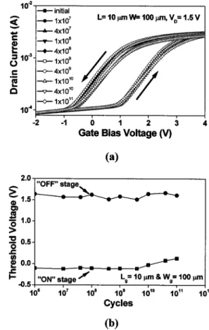
FIG. 5.(a) The endurance characteristics and (b) threshold voltage changes of PTO/Si FeMOSFETs after 1 MHz± 4 V writing with different stress cycles.
Appl. Phys. Lett., Vol. 85, No. 20, 15 November 2004 Sunet al. 4727
This article is copyrighted as indicated in the article. Reuse of AIP content is subject to the terms at: http://scitation.aip.org/termsconditions. Downloaded to IP: 140.113.38.11 On: Thu, 01 May 2014 04:06:30
ward within the time range of 1000 s. Consequently, a reten-tion time of ⬎1000 s can be claimed from the time-independent current values. The good retention could also support the absence of the interfacial layer that not only be-haves as a series capacitor but also generates a depolarization field.
We have further done the measurement of the endurance of 1T PTO/Si memory. Figures 5(a) and 5(b) illustrate the endurance characteristics in ID–VG and ⌬VT of PTO/Si
memory, respectively. The ON and OFF states in VT before
and after stress are determined from the ID–VG hysteresis
loops under the stress condition of ±4 V at 1 MHz. As shown in Fig. 5(a), the nearly identical ID–VGcurves after repeated cycling are in agreement with the good endurance ⬎1011 cycles in Fig. 5(b). This good endurance is attributed to the fact that the low program/erase electric fields could generate the relatively small amount of defects in the PTO/Si memory structure.
In conclusion, a ferroelectric PTO/Si 1T memory with large memory window, high mobility, sharp capacitance change, and good endurance has been demonstrated. Unlike using the buffer layer in stack gate structure, the low tem-perature annealing for the single-layer ferroelectric gate has been proved to be extremely essential in preventing the for-mation of an interfacial layer. The good memory
character-istics in this FeMOSFET show the technical potential for next-generation memory application.
This work has been supported by NSC93-2215-E-009-001 of Taiwan.
1
S. Y. Wu, IEEE Trans. Electron Devices 499(1974).
2
S. Y. Wu, Ferroelectrics 11, 379(1976).
3
S. L. Miller and P. J. McWhorter, J. Appl. Phys. 72, 5999(1992).
4
J.-P. Han and T. P. Ma, Appl. Phys. Lett. 72, 1185(1998).
5
M. Y. Yang, S. B. Chen, A. Chin, C. L. Sun, B. C. Lan, and S. Y. Chen, Tech. Dig. - Int. Electron Devices Meet. 2001, 795(2001).
6
C. L. Sun, S. Y. Chen, S. B. Chen and A. Chin, Appl. Phys. Lett. 80, 3168
(2002).
7
C. L. Sun, S. Y. Chen, M. Y. Yang, and A. Chin, J. Electrochem. Soc. 148, F203(2001).
8
C. L. Sun, S. Y. Chen, S. B. Chen, and A. Chin, Appl. Phys. Lett. 80, 1984(2002).
9
R. Schroeder, L. A. Majewski, and M. Grell, Adv. Mater.(Weinheim,
Ger.) 7, 633 (2004).
10
A. Chin, C. C. Liao, C. H. Lu, W. J. Chen, and C. Tsai, Symposium on
VLSI Technology, 1999, p. 133.
11
A. Chin, Y. H. Wu, S. B. Chen, C. C. Liao, and W. J. Chen, Symposium on
VLSI Technology, 2000, p. 19.
12
K. Onishi, C. S. Kang, R. Choi, H. J. Cho, S. Gopalan, R. Nieh, S. Krishnan, and Jack C. Lee, Symposium on VLSI Technology, 2002, p. 22.
13
C. H. Huang, D. S. Yu, A. Chin, W. J. Chen, C. X. Zhu, M.-F. Li, B. J. Cho, and D. L. Kwong, Tech. Dig. - Int. Electron Devices Meet. 2003, 319.
4728 Appl. Phys. Lett., Vol. 85, No. 20, 15 November 2004 Sunet al.
This article is copyrighted as indicated in the article. Reuse of AIP content is subject to the terms at: http://scitation.aip.org/termsconditions. Downloaded to IP: 140.113.38.11 On: Thu, 01 May 2014 04:06:30