Nanoscale surface electrical properties of indium–tin–oxide films for organic light
emitting diodes investigated by conducting atomic force microscopy
Heh-Nan Lin, Sy-Hann Chen, Gung-Yeong Perng, and Show-An Chen
Citation: Journal of Applied Physics 89, 3976 (2001); doi: 10.1063/1.1353558 View online: http://dx.doi.org/10.1063/1.1353558
View Table of Contents: http://scitation.aip.org/content/aip/journal/jap/89/7?ver=pdfcov
Published by the AIP Publishing
Articles you may be interested in
Work-function changes of treated indium-tin-oxide films for organic light-emitting diodes investigated using scanning surface-potential microscopy
J. Appl. Phys. 97, 073713 (2005); 10.1063/1.1884245
Highly oriented indium tin oxide films for high efficiency organic light-emitting diodes
J. Appl. Phys. 91, 5371 (2002); 10.1063/1.1461068
Electrical, optical, and structural properties of indium–tin–oxide thin films for organic light-emitting devices
J. Appl. Phys. 86, 6451 (1999); 10.1063/1.371708
Surface energy and polarity of treated indium–tin–oxide anodes for polymer light-emitting diodes studied by contact-angle measurements
J. Appl. Phys. 86, 2774 (1999); 10.1063/1.371124
Work function modification of indium–tin–oxide used in organic light emitting devices
J. Vac. Sci. Technol. A 17, 1773 (1999); 10.1116/1.581889
Nanoscale surface electrical properties of indium–tin–oxide films
for organic light emitting diodes investigated by conducting atomic
force microscopy
Heh-Nan Lina)
Department of Materials Science and Engineering, National Tsing Hua University, Hsinchu 300, Taiwan, Republic of China
Sy-Hann Chen
Department of Electrophysics, National Chiao Tung University, Hsinchu 300, Taiwan, Republic of China and Precision Instrument Development Center, National Science Council, Hsinchu 300, Taiwan, Republic of China
Gung-Yeong Perng and Show-An Chen
Department of Chemical Engineering, National Tsing Hua University, Hsinchu 300, Taiwan, Republic of China
共Received 5 September 2000; accepted for publication 12 January 2001兲
Nanoscale surface electrical properties of indium–tin–oxide films prepared by different cleaning methods for use as anode materials in organic light emitting diodes are studied by conducting atomic force microscopy. It is found that most of the surface area possesses a nonconducting feature, and an ultraviolet-ozone treatment produces the most nonconductive sample. The conducting regions, which distribute randomly and range from 6 to 50 nm in size, are attributed to the existence of Sn-rich oxide by a comparison with reported scanning electron microscopy images. After scanning the tip with a bias of ⫺8 V on the nonconducting regions, oxide decomposition occurs on as-received and wet-cleaning processed samples, whereas no structure change appears on the ozone treated sample. The results indicate that the generation of stable oxide after ozone treatment is one of the origins for improved device performance. © 2001 American Institute of Physics. 关DOI: 10.1063/1.1353558兴
I. INTRODUCTION
Organic light emitting diodes共OLEDs兲 have attracted a lot of interest in recent years for their potential to produce low-cost optoelectronic devices.1,2 Due to its transparency and high electrical conductivity, indium–tin–oxide共ITO兲 is usually used as the anode material. Typically, ITO is pro-duced by deposition of a mixture of In2O3共⬃95%–90%兲 and
SnO2 共⬃5%–10%兲, and its high conductivity is due to the
oxygen vacancies in In2O3 and the extra electrons from the
doped Sn atoms.3However, it is well known that the surface properties of ITO, such as the roughness, work function 共WF兲, etc., have a significant influence on device performance.4–6Furthermore, different ITO cleaning proce-dures also change these properties and thus the efficiency achieved.4–6
Since the organic emissive layer typically has a thick-ness of around 100 nm or less, it would be advantageous to have an understanding of the nanoscale electrical properties of ITO. Also, experimental results of such kind will shed light on the microscopic origins of the factors affecting de-vice operation. However, such an endeavor has not been re-alized to our knowledge. In this article, we employ conduct-ing atomic force microscopy共AFM兲7–9to investigate surface electrical properties of ITO films prepared by different clean-ing methods. The results provide evidence that the
produc-tion of stable oxide on ITO contributes to higher efficiency and better stability.
II. EXPERIMENT
The experiment was performed under ambient condi-tions using a commercial AFM 共Dimension 3100, Digital Instruments兲. Rectangular Si tips 共CSC17, NT-MDT, Russia兲 with an estimated spring constant of 0.15 N/m were used in contact mode for simultaneous topography and current mea-surements. The contact force was maintained at around 60 nN as determined from a force–distance plot. The tips were precoated with a Cr layer by the manufacturer and subse-quently coated with a 15 nm Au film by ion sputtering. Bias voltage was applied to the tip through electronics in the AFM and the ITO was grounded. The current was amplified by a preamplifier 共SR-570, Stanford Research Systems兲 and sent to the AFM controller through a signal access module. A 1 k⍀ resistor was put in series for protection.
Commercially available ITO films共SLR, Sanyo Vacuum Industry, Japan兲 with a thickness of around 150 nm on glass substrates were used for experiment. Three samples were tested. Sample A was the as-received specimen. Sample B was cleaned in isopropyl alcohol for 30 min, CH2Cl2 for 30
min, and H2O2/NH4OH/de-ionized water共1:1:5兲 solution for
60 min. Sample C was first cleaned by the same steps as sample B, and then treated by ultraviolet共UV兲-ozone for 60
a兲Electronic mail: [email protected]
3976
0021-8979/2001/89(7)/3976/4/$18.00 © 2001 American Institute of Physics
min. All the above wet cleaning procedures were performed in an ultrasonic bath.
III. RESULTS
With a bias of⫺0.5 V applied to the tip during scanning, the topography共left兲 and current 共right兲 images of the three ITO samples are shown in Fig. 1. Various dot structures ranging from 30 to 90 nm in size are on the surfaces and the root-mean-square roughness values are 1.4, 2.4, and 2.3 nm, respectively. Obviously, the wet cleaning procedure in-creased the surface roughness, whereas the UV-ozone treat-ment had little effect.
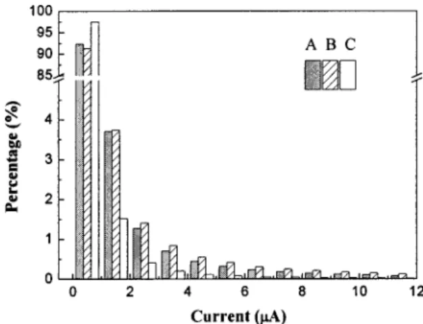
In the current images, conducting and nonconducting re-gions both exist on the surfaces with the former signified by bright contrast. Apparently, most of the surface area has a nonconducting feature. On the other hand, conducting re-gions distribute randomly, with sizes ranging from 6 to 50 nm. The smallest value of 6 nm is confirmed by higher reso-lution images 共not shown兲 and is in reasonable agreement with the estimated tip–sample contact diameter of 7.4 nm obtained from a simple Hertz contact mechanics calculation.10 The percentage of coverage of these two re-gions can be obtained from the current distribution histo-grams, which are plotted in Fig. 2. If we consider the points below 1A nonconducting, 92% of the surface area is non-conducting on samples A and B, and 97% of the surface area
on sample C is nonconducting. The distributions for samples A and B are quite similar, but sample B is slightly more conductive than sample A.
The identities of the conducting and nonconducting re-gions on the ITO surface can be explained by a direct com-parison with scanning electron microscopy results. From a recent study of the surface structures of homemade 共after heat treatment兲 and commercially available ITO films,11 In2O3, SnO, and Sn-rich oxides共Snn⫹1On and Sn2nO2n⫺1兲
are found to be present on the surface, which also indicates the decomposition of SnO2 in the deposition process. Since
Sn-rich oxides have higher conductivities, it is reasonable to correlate the conducting regions in Fig. 1 to Sn-rich oxides and the nonconducting regions to In2O3 or SnO.
Further-more, it can be argued that the slightly higher presence of more conducting regions on sample B compared to on sample A was due to the reduction of SnO since H2O2in an
alkaline solution facilitates reduction. On the other hand, the UV-ozone treatment assisted oxidation of Sn-rich oxides into SnO and made sample C the most nonconductive 共see be-low兲.
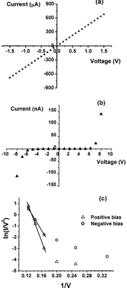
To further verify the above assessments, we also per-formed local current–voltage (I – V) measurements. A typi-cal I – V relationship on the conducting regions of the three samples is shown in Fig. 3共a兲. 共Note that the current is much higher than that in Fig. 1 at bias of 0.5 V, which is due to the formation of a more stable contact in the I – V measurement.兲 From the linear behavior, the contact is apparently an ohmic contact. The point contact resistance is calculated to be around 1.2 k⍀ after subtracting the 1 k⍀ resistance. Two theoretical formalisms can be used to obtain estimates for a comparison. The first is a classical expression for spreading resistance R, which is represented as7,8
R⫽1⫹2
4a , 共1兲
where1 and2 are the resistivities of the two materials in
contact and a the contact radius, which is around 3.7 nm.10 Since the resistivity of ITO is around 3⫻10⫺4⍀ cm,3which is about two orders of magnitude higher than that of Au, Eq. 共1兲 gives a contact resistance of around 200 ⍀. The result is
FIG. 1. Topography共left兲 and current images 共right兲 of 共a兲 the as-received,
共b兲 the wet-cleaning processed, and 共c兲 the wet-cleaning and UV-ozone
treated ITOs. The tip was biased to⫺0.5 V and the ITO was grounded.
FIG. 2. Histograms of the current distribution for the three current images in Fig. 1.
3977 J. Appl. Phys., Vol. 89, No. 7, 1 April 2001 Linet al.
much less than the experimental value. However, a criterion for Eq.共1兲 is that a should be greater than the electron mean free path, which is apparently not fulfilled since the electron mean free path in metals is typically around 10 nm.
A more accurate description of the contact resistance R is Sharvin’s formula,8,9
R⫽ 4
3a2, 共2兲
where is the electron mean free path. Although Eq. 共2兲 holds for nanoscale confinement in a homogeneous material, which is different from our present case, it is still useful for a reasonable estimate. If we use⫽10 nm, the result is 930 ⍀, in good agreement with the experimental result.
A typical I – V curve of the nonconducting regions on sample C is shown in Fig. 3共b兲. The current increases sig-nificantly when the voltage is above 5 V. Apparently, a
Fowler–Nordheim type of electron tunneling6is responsible for the detected current. In this situation, the I – V relation-ship can be linearized and expressed by
ln
冉
IV2
冊
⬀⫺1
V⫹const. 共3兲
To verify this, a plot of ln(I/V2) vs 1/V is shown in Fig. 3共c兲 and a linear relationship is observed at high voltage as ex-pected. Also from Fig. 3共c兲, the tunneling current is higher at a negative tip bias except at the bias of 8 V. This can be explained by the I – V behavior of an asymmetric metal– insulator–metal tunnel diode.12 Since the WFs of ozone-treated ITO and Au are around 4.7 and 5.1 eV, respectively, a higher tunneling current is expected at a large negative tip bias.12
I – V measurements of the nonconducting sites on
samples A and B, however, gave very different results. At the first voltage ramp, the current also increased significantly when the bias was above 5 V. But at the second ramp, the nonconducting sites became conducting and ohmic contact behavior appeared. Various regions on both samples were tested, but a similar phenomenon was observed. To further explore this phenomenon, a high voltage of⫺8 or ⫹8 V was first applied to the tip in a scanning area of 0.5⫻0.5 m2, and a larger area of 3⫻3 m2 was imaged in the second scanning with the tip bias reduced to⫺0.5 V. This measure-ment was performed on samples C and B, and there was no structural change on the former’s surface as expected. The results on sample B are shown in Fig. 4, where a crater with a depth of 30 nm and a hillock with a height of 25 nm are present in Figs. 4共a兲 共⫺8 V兲 and 4共b兲 共⫹8 V兲, respectively. Both the crater and the hillock have similar diameters of around 0.6 m. The current images were not reproducible, which was probably caused by peeloff of the Au film, and are not presented. The crater formation should be related to the decomposition of In2O3 or SnO due to the high electric
field. The hillock formation is possibly related to field evapo-ration of the tip material,13 local oxidation,14 or dielectric
FIG. 3. Typical I – V curves on 共a兲 the conducting regions on the three samples,共b兲 the nonconducting regions on sample C, and 共c兲 the Fowler– Nordheim plot of the absolute I, V values in共b兲. Note that I – V measure-ments on nonconducting regions on samples A and B did not give repro-ducible results.
FIG. 4. Topography images of sample B after the application of tip biases of
共a兲 ⫺8 and 共b兲 ⫹8 V in a prescanning area of 0.5⫻0.5m2. The sizes of the crater in共a兲 and the hillock in 共b兲 are both around 0.6m. The depth in共a兲 and the height in共b兲 are approximately 30 and 25 nm, respectively.
breakdown.15 Details of the mechanisms for the structural change, however, are beyond the scope of the present work.
IV. DISCUSSION
It has so far been evidenced that stable oxide existed on sample C, but not on samples A and B. As a result, it is reasonable to relate the occurrence to more complete oxida-tion after the UV-ozone treatment. The results also shed light on issues related to OLED efficiency and stability. It is widely accepted that UV-ozone or oxygen plasma treated ITOs usually give higher efficiencies than as-received or wet-cleaning processed ones,4–6 which has also been our own experience. The origin is generally attributed to the in-crease in the WF of ITO after such treatments,5,16,17 which thus reduces the energy barrier for hole injection from the ITO to the polymer. The mechanism for the WF increase, however, has not been identified unambiguously.16,17 From our observation, it clearly implies that the WF increase is related to the formation of stable oxide. This assertion is partially consistent with a recent study that connects the WF increase to the oxidation of Sn.17 However, since In2O3 is
dominant on the surface, the formation of stable In2O3
should be the major factor. Our observation also agrees with reports that demonstrate the addition of an ultrathin layer of SiO2 on ITO increases the efficiency of molecule-based
OLEDs.18,19
In addition to creating a boost in efficiency, a sturdy oxide layer also hinders chemical reactions at the interface between the ITO and the organic layer. As has already been described previously, samples A and B are susceptible to oxide decomposition. The metal ions generated can react with the emissive layer and reduce the device lifetime.20,21 On the other hand, metal ions are difficult to generate if the surface oxide is stable, as on sample C. Following this point of view, a stable layer should have a similar effect. It has been confirmed that, by adding a hole transport layer be-tween the ITO and the emissive layer, the degradation is slowed down and the stability is improved.22 It should be mentioned, however, that the ozone treatment did not com-pletely oxidize the ITO surface, as is evident from Fig. 1共c兲. The remaining conducting regions may react with the or-ganic layer and become the possible starting regions of de-vice failure.
V. CONCLUSIONS
In summary, we have performed a nanoscale surface electrical study of ITO films by a conducting AFM. On all the samples, a nonconducting feature is dominant on the sur-face and ohmic contact behavior appears on the conducting regions. With a voltage sweep of up to 8 V, reproducible
field emission type tunneling is observed only on the non-conducting regions on the UV-ozone treated ITO, whereas the decomposition of oxide is observed on the other two samples. Our work suggests that the generation of stable ox-ide on ITO is one of the origins that leads to better device performance.
ACKNOWLEDGMENTS
The authors acknowledge Professor David Paine of Brown University for providing the Young’s modulus of ITO. They also thank Shen-Shen Wang and Ju-Hung Hsu for technical assistance. This work was supported by the Na-tional Science Council of Republic of China 共Grant No. 89-2215-E-007-035兲.
1J. R. Sheats, H. Antoniadis, M. Hueschen, W. Leonard, J. Miller, R. Moon, D. Roitman, and A. Stocking, Science 273, 884共1996兲. 2R. H. Friend et al., Nature共London兲 397, 121 共1999兲. 3
H. Kim, C. M. Gilmore, A. Pique´, J. S. Horwitz, H. Mattoussi, H. Murata, Z. H. Kafafi, and D. B. Chrisey, J. Appl. Phys. 86, 6451共1999兲. 4C. C. Wu, C. I. Wu, J. C. Sturm, and A. Kahn, Appl. Phys. Lett. 70, 1348
共1997兲.
5J. S. Kim, M. Granstro¨m, R. H. Friend, N. Johansson, W. R. Salaneck, R. Daik, W. J. Feast, and F. Cacialli, J. Appl. Phys. 84, 6859共1998兲. 6S. K. So, W. K. Choi, C. H. Cheng, L. M. Leung, and C. F. Kwong, Appl.
Phys. A: Mater. Sci. Process. 68, 447共1999兲.
7S. J. O’Shea, R. M. Atta, M. P. Murrell, and M. E. Welland, J. Vac. Sci. Technol. B 13, 1945共1995兲.
8
M. A. Lantz, S. J. O’Shea, and M. E. Welland, Phys. Rev. B 56, 15345
共1997兲.
9A. Bietsch, M. A. Schneider, M. E. Welland, and B. Michel, J. Vac. Sci. Technol. B 18, 1160共2000兲.
10
From the Hertz model, we have a3⫽3Fr/4E* and 1/E*⫽(1⫺1 2
)/E1
⫹(1⫺2 2
)/E2, where a is the contact radius, F the load, r the tip radius,
E the Young’s modulus, and the Poisson ratio. With F⫽60 nN, r
⫽50 nm, E1⫽81 GPa,1⫽0.42 共for Au兲, and E2⫽80 GPa,2⫽0.2 共for ITO兲, a is determined to be 3.7 nm.
11
T. Nakao, T. Nakada, Y. Nakayama, K. Miyatani, Y. Kimura, Y. Saito, and C. Kaito, Thin Solid Films 370, 155共2000兲.
12S. M. Sze, Physics of Semiconductor Devices共Wiley, New York, 1981兲. 13H. Koyanagi, S. Hosaka, R. Imura, and M. Shirai, Appl. Phys. Lett. 67,
2609共1995兲. 14
E. S. Snow, G. G. Jernigan, and P. M. Campbell, Appl. Phys. Lett. 76, 1782共2000兲.
15N. P. Magtoto, C. Niu, B. M. Ekstrom, S. Addepalli, and J. A. Kelber, Appl. Phys. Lett. 77, 2228共2000兲.
16
K. Sugiyama, H. Ishii, Y. Ouchi, and K. Seki, J. Appl. Phys. 87, 295
共2000兲.
17D. J. Milliron, I. G. Hill, C. Shen, A. Kahn, and J. Schwartz, J. Appl. Phys. 87, 572共2000兲.
18Z. B. Deng, X. M. Ding, S. T. Lee, and W. A. Gambling, Appl. Phys. Lett.
74, 2227共1999兲.
19X. M. Ding, L. M. Hung, L. F. Cheng, Z. B. Deng, X. Y. Hou, C. S. Lee, and S. T. Lee, Appl. Phys. Lett. 76, 2704共2000兲.
20C.-I. Chao, K.-R. Chuang, and S.-A. Chen, Appl. Phys. Lett. 69, 2894
共1996兲.
21
J. Shen, D. Wang, E. Langlois, W. A. Barrow, P. J. Green, C. W. Tang, and J. Shi, Synth. Met. 111–112, 233共2000兲.
22Q. T. Le, F. M. Avendano, E. W. Forsythe, L. Yan, Y. Gao, and C. W. Tang, J. Vac. Sci. Technol. A 17, 2314共1999兲.
3979
J. Appl. Phys., Vol. 89, No. 7, 1 April 2001 Linet al.