The Effect of Preheating Treatment on Anodic A1203 Formed
on Spulfereci Al Thin Films
Re-Long Chiu and Peng-Heng Chang
Insitutes of Materials Science and Engineering, National Chiao Thng University, Hsinchu, Taiwan Chi-Hanglung
ElectronicsResearch and Service Organization, Industrial Technology Research Institute,
Chu-Thng, Taiwan 31015
ABSTRACT
A1203 layers were grown by anodizing Al films sputtered on borophosphosilicate glass/Si02/Si substrates and subse-quently characterized by transmission electron microscopy, and by current-voltage and capacitance-voltage measure-ments using a metal/insulator/metal structure. Amorphous anodic oxide is formed on nonpreannealed Al film but a com-plex oxide film generally consisting of five sublayers (designated as amorphous I, porous I, crystalline, porous II, and amorphous II) is formed on preannealed Al film. Freshly formed anodic oxide is always amorphous in both preannealed and nonpreannealed Al thin films. The growth of the crystalline layer in preannealed samples is due to the amorphous-to-crystalline transition of the amorphous II layer. The porous I layer is formed well before the crystalline layer. The voids in this layer are probably due to the trapping of oxygen at the sites of crystalline oxide. The voids in the porous II layer are small and their formation can be attributed to the volume shrinkage associated with the amorphous-to-crystalline transition of the amorphous II layer. The amorphous oxide films exhibit excellent dielectric properties. The dielectric properties of the complex oxide are much inferior and vary significantly due to structural variation.
Introduction
Thepropensity of hillock formation in thin film Al metal on Si02 substrate during thermal process has, until
recent-ly, prevented its application in thin film transistors
(TFT)/liquid crystal display (LCD). However, a recent report of using anodic aluminum oxide as a protective
coating against hillock formation has prompted renewed interest in Al metallization for TFT/LCD. 1The primary advantage of Al over the conventional Cr or Ta
metalliza-tion in TFT/LCD is its low resistivity that results in
reduced gate pulse delay and wave form distortion,23 a necessity for making large size, high resolution LCD.
Additionally, the well-established process technology and integrated circuit (IC) compatibility of Al metallization is also welcome from processing point of view.
The anodic A1203 oxide for IC applications is typically an impervious barrier film produced by a nonsolvent elec-trolyte that does not dissolve oxide.4'5 The structure of the barrier-type anodic A1203 oxide film may be either amor-phous, crystalline, or a mixture of both, depending on the anodizing conditions.6-8 The properties of anodic oxide is
significantly affected by its structure, and generally the
amorphous A1203 films exhibit better dielectric properties than the crystalline and mixed films.89 The surface condi-tion of the Al metal prior to anodizing is one of the impor-tant factors in determining the anodic oxide structure.5'1°
Aluminum is easily oxidized in air so that a thin
air-formed native oxide is often present on the surface.'°'11 Deliberate thermal treatment of Al, especially at
tempera-tures higher than 400°C, can induce crystalline A1203
nuclei to form on the surface.6'11'4 The nature of the crys-talline nuclei is not yet clear, but the spinel -y-phase has been suspected." The nuclei grown into isolated lenticular clusters frequently accompanied with voids during subse-quent anodizing and thier crystal structure has been
con-firmed to -y'-A1203.1114 Both -y- and -y'-A1203 have a
closed-packed oxygen lattice, their structures differ only in the
degree of ordering in the positions of the aluminum
atoms.° Since the growth of barrier anodic A1203 oxide
occurs at both electrolyte/oxide and oxide/metal
inter-faces,'5 the lenticular -y'--crystallites are always observed to be dispersed near the centerline of the oxide film where
the original top surface is located. Prolonged anodizing
caused the -y'-crystallites to grow laterally and eventually
*ElectrochemicalSociety Active Member.
a crystalline layer sandwiched betwen amorphous oxide may be formed.614 In contrast, crystalline A1203 grown by
thermal oxidation of Al metal at elevated temperature
(400 to 600°C), either in air16 or in vacuum,'617 is predomi-nantly the y-phase. The morphology varies with the
orien-tation of the underlying Al substrate, being elongated platelets on (11 0),16 triangular-hexagonal platelets on
(111)16 andsquare17 or trianglular-hexagonal platelets on
(100).16Voidsare not observed with the crystalline oxide
formed by thermal oxidation.
While most of the previous studies were made on alu-minum sheets, it is of great interest to study the anodizing
of Al thin films used for IC applications. In previous
papers we have studied the effects of 1% Si and 0.5% Cu doping14 and of electrolyte temperature'8 on the structure and properties of anodic oxide films formed on sputtered thin Al metal films. In this paper the effect of pretreatment is studied in detail.
Experiment
Thesubstrates for the present study were 4 in. diam p-type, <100>, Si wafers. To simulate a typical glass
sub-strate used for LCD, a 550 nm thermal oxide was first
grown on the substrate and a 600 nm thick
borophospho-silicate glass (BPSG) was subsequently deposited by
chemical vapor deposition at 720°C. A 300 nm thick Al film was deposited in a dc magnetron sputtering deposi-tion machine from a pure Al target on top of the borophos-phosilicate glass (BPSG) 5i02/Si substrates. To investigate the effect of preannealing on the anodic oxide formation, two series of samples were prepared. For the first series, the wafers were anodized directly after the metal deposi-tion. For the second series, the wafers were annealed at 410°C for 30 mm in a nitrogen (99.99995%, oxygen content 0.1 —0.2ppm) ambient prior to anodizing. For both series,
the A1203 dielectric layer was grown by anodizing the
wafers, one at a time, at room temperature in an acid-gly-col-water (AGW) electrolyte that is a mixture of 3% aque-ous solution of tartaric acid and propylene glycol at a vol-ume ratio of 2:8. The cathode was plain stainless steel and
typically about 90% of the wafer was immersed in the
electrolyte while the exposed region was connected to the anode through a Cu clamp. Anodization was controlled by
a programmable Keithley 237 current/voltage
source-measure unit interfaced to a personal computer.
Anodization was conducted in constant current mode
(current density =0.4mA/cm2) initially and was switched 984 J. Efectrochem. Soc., Vol. 143, No. 3, March 1996 The Etectrochemical Society, Inc.
The Effect of Preheating Treatment on Anodic A1203 Formed
on Spulfered Al Thin Films
Re-Long Chiu andPeng-Heng Chang
Insitutes of Materials Science and Engineering, National Chiao Tang University, Hsinchu, Taiwan Chi-Hanglung
ElectronicsResearch and Service Organization, Industrial Technology Research Institute,
Chu-Tung, Taiwan 31015
ABSTRACT
Al,03 layers were grown by anodizing Al films sputtered on borophosphosilicate glass/SiO,/Si substrates and subse-quently characterized by transmission electron microscopy, and by current-voltage and capacitance-voltage measure-ments using a metal/insulator/metal structure. Amorphous anodic oxide is formed on nonpreannealed Al film but a com-plex oxide film generally consisting of five sublayers (designated as amorphous I, porous I, crystalline, porous II, and amorphous II) is formed on preannealed Al film. Freshly formed anodic oxide is always amorphous in both preannealed and nonpreannealed Al thin films. The growth of the crystalline layer in preannealed samples is due to the amorphous-to-crystalline transition of the amorphous II layer. The porous I layer is formed well before the crystalline layer. The voids in this layer are probably due to the trapping of oxygen at the sites of crystalline oxide. The voids in the porous II layer are small and their formation can be attributed to the volume shrinkage associated with the amorphous-to-crystalline transition of the amorphous II layer. The amorphous oxide films exhibit excellent dielectric properties. The dielectric properties of the complex oxide are much inferior and vary significantly due to structural variation,
Introduction
Thepropensity of hillock formation in thin film Al metal on Si02 substrate during thermal process has, until
recent-ly, prevented its application in thin film transistors
(TFT)/liquid crystal display (LCD). However, a recent report of using anodic aluminum oxide as a protective
coating against hillock formation has prompted renewed
interest in Al metallization for TFT/LCD. The primary
advantage of Al over the conventional Cr or Ta
metalliza-tion in TFT/LCD is its low resistivity that results in
reduced gate pulse delay and wave form distortion,2'3 anecessity for making large size, high resolution LCD.
Additionally, the well-established process technology and integrated circuit (IC) compatibility of Al metallization is also welcome from processing point of view.
The anodic A1203 oxide for IC applications is typically an impervious barrier film produced by a nonsolvent elec-trolyte that does not dissolve oxide.4'5 The structure of the barrier-type anodic Al203 oxide film may be either amor-phous, crystalline, or a mixture of both, depending on the anodizing conditions.6-' The properties of anodic oxide is
significantly affected by its structure, and generally the
amorphous Al,O, films exhibit better dielectric properties than the crystalline and mixed films." The surface condi-tion of the Al metal prior to anodizing is one of the impor-tant factors in determining the anodic oxide structure.5"
Aluminum is easily oxidized in air so that a thin air-formed native oxide is often present on the surface."
Deliberate thermal treatment of Al, especially at
tempera-tures higher than 400°C, can induce crystalline Al20, nuclei to form on the surface."" The nature of the crys-talline nuclei is not yet clear but the spinel 7-phase has
been suspected." The nuclei grown into isolated lenticular clusters frequently accompanied with voids during subse-quent anodizing and thier crystal structure has been con-firmed to -y'-Al,O,."" Both -y- and -y'-Al,03 have a closed-packed oxygen lattice, their structures differ only in the
degree of ordering in the positions of the aluminum
atoms.' Since the growth of barrier anodic A1,O, oxide occurs at both electrolyte/oxide and oxide/metal
inter-faces,'5 the lenticular -y'-crystallites are always observed to be dispersed near the centerline of the oxide film where
the original top surface is located. Prolonged anodizing
caused the -y'-crystallites to grow laterally and eventually
*ElectrochemicalSociety Active Member.
a crystalline layer sandwiched betwen amorphous oxide may be formed.''4 In contrast, crystalline A120, grown by
thermal oxidation of Al metal at elevated temperature
(400 to 600°C), either in air'6 or in vacuum,'6"7 is predomi-nantly the y-phase. The morphology varies with the
orien-tation of the underlying Al substrate, being elongated platelets on (110)," triangular-hexagonal platelets on
and square" or trianglular-hexagonal platelets on (100)." Voids are not observed with the crystalline oxide formed by thermal oxidation.
While most of the previous studies were made on alu-minum sheets, it is of great interest to study the anodizing
of Al thin films used for IC applications. In previous
papers we have studied the effects of 1% Si and 0.5% Cu doping'4 and of electrolyte on the structure and properties of anodic oxide films formed on sputtered thin Al metal films. In this paper the effect of pretreatment is studied in detail.
Experiment
Thesubstrates for the present study were 4 in. diam p-type, <100>, Si wafers. To simulate a typical glass
sub-strate used for LCD, a 550 nm thermal oxide was first
grown on the substrate and a 600 nm thick
borophospho-silicate glass (BPSG) was subsequently deposited by
chemical vapor deposition at 720°C, A 300 nm thick Al film was deposited in a dc magnetron sputtering deposi-tion machine from a pure Al target on top of the borophos-phosilicate glass (BPSG) SiO,/Si substrates. To investigate the effect of preannealing on the anodic oxide formation, two series of samples were prepared. For the first series, the wafers were anodized directly after the metal deposi-tion, For the second series, the wafers were annealed at 410°C for 30 mm in a nitrogen (99.99995%, oxygen content 0.1 -'0.2ppm) ambient prior to anodizing. For both series,
the Al,03 dielectric layer was grown by anodizing the
wafers, one at a time, at room temperature in an acid-gly-col-water (AGW) electrolyte that is a mixture of 3% aque-ous solution of tartaric acid and propylene glycol at a vol-ume ratio of 2:8. The cathode was plain stainless steel and
typically about 90% of the wafer was immersed in the
electrolyte while the exposed region was connected to the anode through a Cu clamp. Anodization was controlled by
a programmable Keithley 237 current/voltage
source-measure unit interfaced to a personal computer.
Anodization was conducted in constant current mode
(current density =0.4mA/cm') initially and was switched 984 J. Electrochem. Soc., Vol. 143, No.3, March 1996 Electrochemical Society, Inc.
J Electrochem. Soc., Vol. 143, No.3, March 1996 The Electrochemical Society, Inc. 985 to constant voltage mode automatically when the voltage
reached 100 V To investigate the structure of the oxide
films formed at different stages of anodization specimens were anodized for different duration varying from 3.5 to
40 mm and characterized subsequently by transmission
electron microscopy (TEM). TEM samples were prepared by ion milling in the usual fashion'9 and examined within a Philips CM2O microscope operating at 200 kV. High
res-olution TEM work was performed with a JEOL 4000
microscope operating at 400 kV The thickness of the anod-ic films was measured both by TEM and by ellipsometry using a Rudolph Research Auto EL-ILL ellipsometer with He-Ne laser at the wavelength of 632.8 nm. The dielectric properties of the anodic oxide films formed on both
pre-annealed and nonprepre-annealed wafers after 40 mm
anodization were also studied by current-voltage (I- V) andcapacitance-voltage (C-V) measurements
using a
metal/insulator/metal (MIM) structure. To fabricate theMIM capacitors, a 400 nm thick Al film was further deposited by dc magnetron sputtering on the anodized
wafers. The capacitor electrodes, 200 X200 sm squares, were defined using standard lithography and reactive ion etching. The I-V measurements were carried out with a HP
4145B semiconductor parameter analyzer and the high frequency (1 MHz) capacitance measurement was
per-formed using a Keithley 82 c-v system. Resultand Discussion
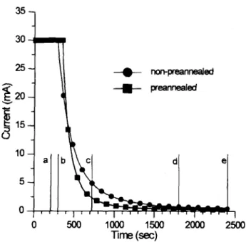
Thevariations of the anodizing voltage and anodizing current with time are shown in Fig. 1 and 2, for the prean-nealed and nonpreanprean-nealed samples, respectively. The
ini-tial rise of voltage in Fig. 1 corresponds to the constant
current anodization. The initial zero-time voltage is sensi-tive to the process history prior to anodizing. The fact that the preannealed sample requires a lower voltage during the constant current anodization indicates that patches of thin oxide regions had already formed on the metal
sur-face during preannealing thus reducing the clean metal
area so that a lower applied voltage is required relative to the nonpreannealed sample in order to maintain the same current density. The rate of increase in voltage (defined as
voltage growth rate) during the constant current period
varies slightly for the two samples, being 0.206 v/s for the nonpreannealed sample and 0.214 v/s for the preannealed one. In Fig. 2, the sudden drop of the anodic current at 30 mA signifies the onset of constant voltage mode (i.e., the
voltage has reached 100 V). Apparently, for the prean-nealed sample the anodizing voltage reaches 100 v at a later time, but the current decreases more sharply and
Fig. 1. The variation of anodizing voltage with time.
2500
eventually reaches a lower minimum residual current in
this sample than the nonpreannealed sample. The total
electrical charge consumed during anodizing is equal to the area under the I-t curve and is 15.8 and 17.4 c for the
preannealed and nonpreannealed sample, respectively.
The amount of oxide formed on the sample is
proportion-al to the quantity of charge consumed; assuming equproportion-al
current efficiency this implies that the capacitance of the preannealed sample may be lower than the nonpreanriealed sample.
The current efficiency for the anodizing process may be
estimated from the total charge consumed and the
vol-ume of the oxide formed. The total electrical charge
con-sumed can be calculated from the area under the I-t
curve in Fig. 2 and the volume of the oxide layer can be measured from the TEM micrographs shown in Fig. 3 and4. (For oxide films containing voids the volume of the voids is subtracted from the total volume of the oxide
film.) An oxide density of 3.1 and 3.6 g/cm3 is assumed for the amorphous2° and crystalline2' anodic aluminum oxide,
respectively. The calculated current efficiency for the oxide formation is 97% for the nonpreannealed sample
and 87% for the preannealed sample. The lower efficiency for the preannealed sample is not unexpected in view of the large amount of defects, such as voids and crystallites, formed in the oxide films.
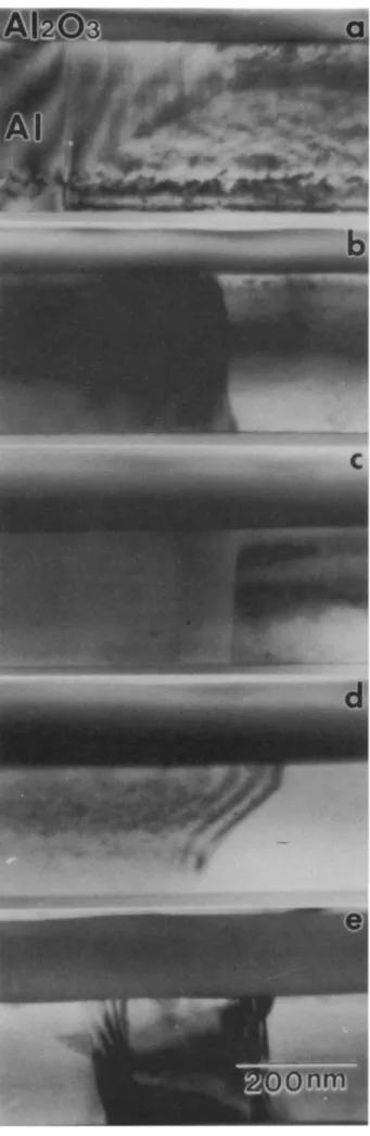
The cross-sectional TEM (XTEM) micrographs of the nonpreannealed oxide films anodized for different dura-tions are shown in Fig. 3. These oxide films are basically
featureless implying an amorphous structure, the
microstructure of the preannealed oxide films anodized
for 210, 300, 720, 1800, and 2400 s are shown in Fig. 4a, b, c, d, and e, respectively. (These samples are corresponding to the vertical lines marked as a, b, c, d, and e in Fig. 1 and Fig. 2, respectively.) In contrast to the oxide films formed in the nonpreannealed samples the oxide films in the
pre-annealed samples are much more complex. Generally
speaking they are composed of five layers designated, from the top to the bottom, as amorphous I, void I, crystalline, void II, and amorphous II layers as labeled in Fig. 4d. It is
well known that anodic aluminum oxide grows at both electrolyte/oxide and oxide/metal interfaces due to the
outward transport of Al ions and the inward transport of oxygen ions.1022'23 The fact that the oxide structure at these two interfaces (i.e., the amorphous I and amorphous II layer, respectively) is amorphous all the time indicates that the freshly formed anodic Al oxide is always amorphous. The void I layer contains many small voids initially (Fig. 4a) and
35 —.--- non-preannealed —-- preannealed C; 10 5 0 0 500 1000 1500 2000 2500 Time(sec)
Fig.2. The variation of anodizing current with time.
120 100
16
6O
40
• Non-prnSed
- Prearneaed 0500 1000
1500 2000
Time (sec)
J Electrochem. Soc., Vol. 143, No.3, March 1996 The Electrochemical Society, Inc. 985 to constant voltage mode automatically when the voltage
reached 100 V. To investigate the structure of the oxide films formed at different stages of anodization specimens were anodized for different duration varying from 3.5 to
40 mm and characterized subsequently by transmission
electron microscopy (TEM). TEM samples were prepared by ion milling in the usual fashion'9 and examined within a Philips CM2O microscope operating at 200 kV. High
res-olution TEM work was performed with a JEOL 4000
microscope operating at 400 kV. The thickness of the anod-ic films was measured both by TEM and by ellipsometry using a Rudolph Research Auto EL-ILL ellipsometer with He-Ne laser at the wavelength of 632.8 nm. The dielectric properties of the anodic oxide films formed on both
pre-annealed and nonprepre-annealed wafers after 40 mm
anodization were also studied by current-voltage (I- V) andcapacitance-voltage (C-V) measurements
using a
metal/insulator/metal (MIM) structure. To fabricate theMIM capacitors, a 400 nm thick Al film was further deposited by dc magnetron sputtering on the anodized
wafers. The capacitor electrodes, 200 X200 sm squares, were defined using standard lithography and reactive ion etching. The I-V measurements were carried out with a HP
4145B semiconductor parameter analyzer and the high frequency (1 MHz) capacitance measurement was
per-formed using a Keithley 82 C-V system. Resultand Discussion
Thevariations of the anodizing voltage and anodizing current with time are shown in Fig. 1 and 2, for the prean-nealed and nonpreanprean-nealed samples, respectively. The
ini-tial rise of voltage in Fig. 1 corresponds to the constant
current anodization. The initial zero-time voltage is sensi-tive to the process history prior to anodizing. The fact that the preannealed sample requires a lower voltage during the constant current anodization indicates that patches of thin oxide regions had already formed on the metal
sur-face during preannealing thus reducing the clean metal
area so that a lower applied voltage is required relative to the nonpreannealed sample in order to maintain the same current density. The rate of increase in voltage (defined as
voltage growth rate) during the constant current period
varies slightly for the two samples, being 0.206 V/s for the nonpreannealed sample and 0.214 V/s for the preannealed one. In Fig. 2, the sudden drop of the anodic current at 30 mA signifies the onset of constant voltage mode (i.e., the
voltage has reached 100 V). Apparently, for the
prean-nealed sample the anodizing voltage reaches 100 V at a
later time, but the current decreases more sharply and
Fig. 1. The variation of anodizing voltage with time.
2500
eventually reaches a lower minimum residual current in
this sample than the nonpreannealed sample. The total
electrical charge consumed during anodizing is equal to the area under the I-t curve and is 15.8 and 17.4 C for the
preannealed and nonpreannealed sample, respectively.
The amount of oxide formed on the sample is
proportion-al to the quantity of charge consumed; assuming equproportion-al
current efficiency this implies that the capacitance of the preannealed sample may be lower than the nonpreannealed sample.
The current efficiency for the anodizing process may be
estimated from the total charge consumed and the
vol-ume of the oxide formed. The total electrical charge
con-sumed can be calculated from the area under the I-t
curve in Fig. 2 and the volume of the oxide layer can be measured from the TEM micrographs shown in Fig. 3 and4. (For oxide films containing voids the volume of the voids is subtracted from the total volume of the oxide
film.) An oxide density of 3.1 and 3.6 g/cm3 is assumed for the amorphous2° and crystalline2' anodic aluminum oxide,
respectively. The calculated current efficiency for the oxide formation is 97% for the nonpreannealed sample
and 87% for the preannealed sample. The lower efficiency for the preannealed sample is not unexpected in view of the large amount of defects, such as voids and crystallites, formed in the oxide films.
The cross-sectional TEM (XTEM) micrographs of the nonpreannealed oxide films anodized for different dura-tions are shown in Fig. 3. These oxide films are basically
featureless implying an amorphous structure, the
microstructure of the preannealed oxide films anodized
for 210, 300, 720, 1800, and 2400 s are shown in Fig. 4a, b, c, d, and e, respectively. (These samples are corresponding to the vertical lines marked as a, b, c, d, and e in Fig. 1 and Fig. 2, respectively.) In contrast to the oxide films formed in the nonpreannealed samples the oxide films in the
pre-annealed samples are much more complex. Generally
speaking they are composed of five layers designated, from the top to the bottom, as amorphous I, void I, crystalline, void II, and amorphous II layers as labeled in Fig. 4d. It is
well known that anodic aluminum oxide grows at both electrolyte/oxide and oxide/metal interfaces due to the
outward transport of Al ions and the inward transport of oxygen ions.10'22'23 The fact that the oxide structure at these two interfaces (i.e., the amorphous I and amorphous II layer, respectively) is amorphous all the time indicates that the freshly formed anodic Al oxide is always amorphous. The void I layer contains many small voids initially (Fig. 4a) and
35 —.--- non-preannealed —-- preannealed C; 5 0 0 500 1000 1500 2000 2500 lime (sec)
Fig. 2. The variation of anodizing current with time.
120 100
160
60
40• Non-prnSed
- Preameeled 0500 1000 1500 2000
Time (sec)986 J. Electrochem. Soc., Vol. 143, No.3, March 1996 The Electrochemical Society, Inc.
Fig. 3. Cross-sectional TEM micrographs of Al203 films
formed on nonpreannealed Al metal films. The anodizing time was (a) 210, (b) 300, (c) 720, (d) 1800, and (e) 2400 s.
Fig. 4. Cross-sectional TEM micrographs of A1203 films formed on preannealed Al metal films. The anodizing time was (a) 210,
(b) 300, (c) 720, (dl 1800, and (e) 2400 s.
c
'lr* !;
.S
—- .. .. 986 J. Electrochem. Soc., Vol. 143, No.3, March 1996 The Electrochemical Society, Inc.
Fig. 3. Cross-sectional TEM micrographs of Al203 films
formed on nonpreannealed Al metal films. The anodizing time was (a) 210, (b) 300, (c) 720, (d) 1800, and (e) 2400 s.
Fig. 4. Cross-sectional TEM micrographs of A1203 films formed on preannealed Al metal films. The anodizing time was (a) 210,
(b) 300, (c) 720, (dl 1800, and (e) 2400 s.
c
'lr* !;
.S
—the number of voids increases on further anodizing under constant current condition (Fig. 4b). Significant void coa—
lescence is observed under constant voltage condition
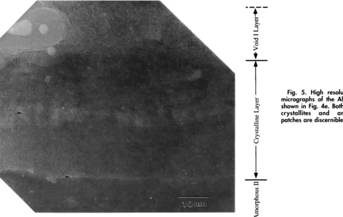
(Fig. 4c, d, and e). Figure 5 shows a cross-sectional high res-olution TEM (HRTEM) micrograph of the oxide film taken from the same TEM specimen shown in Fig. 4d. The
talline layer is marked in this micrograph and its
crys-tallinity is confirmed by the faint lattice fringes revealed. Our previous study'4 has identified the crystallites as
y'-Al,03.
A
large void belonging to the void I layer is observedin contact with the crystalline layer in Fig. 5. The area
neighboring this void appears to be amorphous but lattice fringes are visible further to the right of the void. This sug-gests that the void I layer is a mixed amorphous + crys-talline layer laden with voids. The micrographs in Fig. 4
show clearly that the crystalline layer is always formed beneath the void I layer, but its relative position with
respect to the void II layer varies. Initially the crystalline layer is on top of the void II layer as shown in Fig. 4b, but
as the crystalline layer grows thicker the void II layer
becomes either at the bottom or inside of the crystalline layer as revealed clearly in Fig. 4d (as well as in Fig. 4c and e). The two lighter bands in Fig. 5, one near the
cen-ter and the other at the bottom of the crystalline layer
(marked by arrow), correspond to the voids in the void II layer in Fig. 4d.
It should be emphasized that voids are formed only in
the preannealed samples but not in the nonpreannealed
samples in the present investigation although exactly the
same anodizing conditions were used for both cases. Similar voids have also been reported in anodic
alu-minum oxide formed on preannealed Al-i weight percent (w/o) Si-0.5 w/o Cu thin films'4 and on preannealed alu-minum foils anodized in various electrolytes such as tar-taric acjd,'4 ammonium pentaborate,7'2 and ammonium borate,24 etc. The formation of voids in anodic aluminum oxide is apparently independent of anodizing electrolytes and substrate composition but depends on preannealing
treatment and electrolyte temperature.'8 It has been
shown convincingly6'0'3 that preannealing causes crys-talline -y-A1203 nuclei to form on the surface of aluminum which eventually develop into a crystalline layer during subsequent anodic growth. Since the void I layer is fully4
(1
0
developed even before the formation of the crystalline layer (comparing, for example, Fig. 4a and 4b), the origin of the voids in the void I layer in our preannealed samples
cannot be ascribed to the volume shrinkage associated
with the amorphous to crystalline transition of the
exist-ing amorphous oxide.6 These voids are most likely the result of oxygen trapped near the y'-Al203 crystallites
which eventually form gas bubbles.7
The nature of void II layer is quite different from void I layer. In Fig. 4a we see that this layer has not formed yet. It forms only after the appearance of the crystalline layer
in Fig. 4b, and the voids in this layer are much smaller
compared with those in the void I layer. The voids in the void II layer may be due to the volume shrinkage accom-panied the amorphous to crystalline transition.
The thickness of each individual layer in Fig. 4 can be
measured directly off the micrographs and the data are summarized in Table I. It is worth pointing out that, in order to eliminate any error in the thickness
measure-ment, the TEM specimens were tilted such that the <hO> zone axis of the substrate silicon is aligned to the incident beam direction. This ensures that the oxide layers shown in Fig. 3 and 4 are viewed in the end-on fashion. Also, the
magnifications of TEM micrographs were calibrated
against a standard specimen.
It should be borne in mind in discussing Table I that the
anodizing process in the present study consists of two
regimes, a constant current regime followed by a constant voltage regime. Figure 6 shows the variation of the total
thickness of the oxide layer (the data shown in the last row of Table I) as a function of anodizing time. The switch-over from the constant current mode to the
con-stant voltage mode is marked by the vertical dashed line in Fig. 6. Despite the vast difference in the microstructure
of the preannealed and nonpreannealed, the thickness
variation of the oxide films formed on these two types of samples are quite similar as shown in Fig. 6. The initial portions of the two curves in Fig. 6 (corresponding to the
constant current regime) are practically
indistinguish-able. Only at the end of the anodizing the oxide thickness
in the nonpreannealed samples appears slightly higher
than those in the preannealed samples. The growth rate of
the anodic aluminum oxide is aobut 0.34 nm/s initially
J. Electrochem. Soc., Vol. 143, No.3, March 1996 The Electrochemical Society, Inc. 987
Fig. 5. High resolution TEM
micrographsof the A1203 layer shown in Fig. 4e. Both y'-AI2O3
crystallites and amorphous
patches are disernible.
the number of voids increases on further anodizing under constant current condition (Fig. 4b). Significant void coa—
lescence is observed under constant voltage condition
(Fig. 4c, d, and e). Figure 5 shows a cross-sectional high res-olution TEM (HRTEM) micrograph of the oxide film taken from the same TEM specimen shown in Fig. 4d. The
talline layer is marked in this micrograph and its
crys-tallinity is confirmed by the faint lattice fringes revealed. Our previous study'4 has identified the crystallites as
y'-Al,03.
A
large void belonging to the void I layer is observedin contact with the crystalline layer in Fig. 5. The area
neighboring this void appears to be amorphous but lattice fringes are visible further to the right of the void. This sug-gests that the void I layer is a mixed amorphous + crys-talline layer laden with voids. The micrographs in Fig. 4
show clearly that the crystalline layer is always formed beneath the void I layer, but its relative position with
respect to the void II layer varies. Initially the crystalline layer is on top of the void II layer as shown in Fig. 4b, but
as the crystalline layer grows thicker the void II layer
becomes either at the bottom or inside of the crystalline layer as revealed clearly in Fig. 4d (as well as in Fig. 4c and e). The two lighter bands in Fig. 5, one near the
cen-ter and the other at the bottom of the crystalline layer
(marked by arrow), correspond to the voids in the void II layer in Fig. 4d.
It should be emphasized that voids are formed only in
the preannealed samples but not in the nonpreannealed
samples in the present investigation although exactly the
same anodizing conditions were used for both cases. Similar voids have also been reported in anodic
alu-minum oxide formed on preannealed Al-i weight percent (w/o) Si-0.5 w/o Cu thin films'4 and on preannealed alu-minum foils anodized in various electrolytes such as tar-taric acjd,'4 ammonium pentaborate,7'2 and ammonium borate,24 etc. The formation of voids in anodic aluminum oxide is apparently independent of anodizing electrolytes and substrate composition but depends on preannealing
treatment and electrolyte temperature.'8 It has been
shown convincingly6'0'3 that preannealing causes crys-talline -y-A1203 nuclei to form on the surface of aluminum which eventually develop into a crystalline layer during subsequent anodic growth. Since the void I layer is fully4
(1
0
developed even before the formation of the crystalline layer (comparing, for example, Fig. 4a and 4b), the origin of the voids in the void I layer in our preannealed samples
cannot be ascribed to the volume shrinkage associated
with the amorphous to crystalline transition of the
exist-ing amorphous oxide.6 These voids are most likely the result of oxygen trapped near the y'-Al203 crystallites
which eventually form gas bubbles.7
The nature of void II layer is quite different from void I layer. In Fig. 4a we see that this layer has not formed yet. It forms only after the appearance of the crystalline layer
in Fig. 4b, and the voids in this layer are much smaller
compared with those in the void I layer. The voids in the void II layer may be due to the volume shrinkage accom-panied the amorphous to crystalline transition.
The thickness of each individual layer in Fig. 4 can be
measured directly off the micrographs and the data are summarized in Table I. It is worth pointing out that, in order to eliminate any error in the thickness
measure-ment, the TEM specimens were tilted such that the <hO> zone axis of the substrate silicon is aligned to the incident beam direction. This ensures that the oxide layers shown in Fig. 3 and 4 are viewed in the end-on fashion. Also, the
magnifications of TEM micrographs were calibrated
against a standard specimen.
It should be borne in mind in discussing Table I that the
anodizing process in the present study consists of two
regimes, a constant current regime followed by a constant voltage regime. Figure 6 shows the variation of the total
thickness of the oxide layer (the data shown in the last row of Table I) as a function of anodizing time. The switch-over from the constant current mode to the
con-stant voltage mode is marked by the vertical dashed line in Fig. 6. Despite the vast difference in the microstructure
of the preannealed and nonpreannealed, the thickness
variation of the oxide films formed on these two types of samples are quite similar as shown in Fig. 6. The initial portions of the two curves in Fig. 6 (corresponding to the
constant current regime) are practically
indistinguish-able. Only at the end of the anodizing the oxide thickness
in the nonpreannealed samples appears slightly higher
than those in the preannealed samples. The growth rate of
the anodic aluminum oxide is aobut 0.34 nm/s initially
J. Electrochem. Soc., Vol. 143, No.3, March 1996 The Electrochemical Society, Inc. 987
Fig. 5. High resolution TEM
micrographsof the A1203 layer shown in Fig. 4e. Both y'-AI2O3
crystallites and amorphous
988 J. Electrochem. Soc., Vol. 143, No. 3, March 1996 The Electrochemical Society, Inc.
Table I. Layer thickness of the A1203 films anodized for different time.
during the constant current regime as determined from the slope of the curves in Fig. 6. The growth continues though at an ever decreasing rate even after switching
over to the constant voltage mode and eventually comes to a halt as indicated by the plateau of the curves.
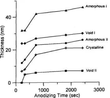
It is of particular interest to know how each of the five
individual layers in the anodic oxide film varies with anodizing time in order to better understand the struc-tural evolution during anodizing. For this purpose, the
individual layer thickness is plotted as a function of time
in Fig. 7. Close examination of this figure reveals the
following.
1. The amorphous I, amorphous II, and crystalline lay-ers exhibit similar growth behavior, namely, fast growth at roughly the same rate (0.024 nm/s) initially up to 720 s followed by very slow growth thereafter when anodizing is well into the constant voltage regime.
2. The void IT layer is not formed initially (even after 210 s), but it grows very rapidly to 5 nm in 90 s (from 210 to 300 s). The thickness is not changed much
subsequent-ly, saturating at about 7 nm eventually. Note that the
growth of this layer occurs mostly during constant cur— rent regime.
3. The void I layer exhibits somewhat different
behav-ior from other layers. This layer grows to 24 nm thick
after 210 s and then its thickness increases only slightly thereafter. In other words, the growth of the void I layer
starts at a very early stage of the constant current regime and does not show a significant increase in thickness dur-ing the initial stage of the constant voltage regime as in
the case of amorphous I, amorphous II, and crystalline
layers. We have shown earlier in reference to Fig. 5 that
void I layer is actually a mixed layer containing amor-phous +crystallineoxide and voids. Although the
thick-ness of void I layer does not change significantly as
anodization proceeds, the amounts of voids in the layer do increase as clearly revealed in Fig. 4.4. In terms of growth rate Fig. 7 shows clearly that
void I> amorphous I> amorphous II >crystalline>void
II. In terms of layer thickness, however, the most domi-nant features in the anodic Al oxide films are amorphous I and void I layer.
The thickening of the crystalline layer during anodizing may be caused by either or the combination of the
follow-ing three mechanisms: (i) the gradual crystallization of the already formed amorphous I layer (ii) the gradual
crystallization of the already formed amorphous II layer, and/or (iii) the reaction of indiffusing oxygen and
out-dif-fusing Al inside the crytalline layer.
In view of the fact that the crystalline layer and the
amorphous I layer are always separated by a void I layer (see Fig. 4) the first mechanism seems to be unlikely to operate. For otherwise one should have observed the
crys-talline layer outgrows the void I layer so that the void I
layer is inside the crystalline layer. The third mechanism, although attractive, is nevertheless inconsistent with the
well-established theory of anodic aluminum oxide
growth, namely, the oxide is grown at two interfaces (electrolyte/oxide and oxide metal interfaces) but not
inside of the existing oxide layer.15 This leaves us with no
choice but to look at the second mechanism. First, it is
interesting to point out that this mechanism is consistent
with the results of other studies that crystallization of
amorphous anodic aluminum oxide tends to occur at the
bottpm half of the oxide layer.1° This phenomenon has
been shown to be related to the anion incorporation from the forming electrolyte. The incorporated anions are
typ-ically found only at the top half of the oxide layer and
I I
1000 2000 3000
Anodizing Time (sec)
Fig. 6. The variation of total thickness of oxide layer as a func-tion of anodizing time.
Fig. 7. The variation of individual layer thickness as a function of anodizing time for the preannealed samples.
Preannealed Films
Thickness (nm)
Const. current Const. voltage
210 (s) 300 (s) 720 (s) 1800 (s) 2400 (s) Layer Type 1 Amorphous I 32 32 42 44 46 2 Voidl 24 24 27 29 30 3 4 Crystalline VoidIl 7 0 8 5 17 6 21 7 21 7 5 Amorphous II 12 14 23 24 26 Total thickness 75 83 115 125 130 Nonpreannealed films 69 79 125 133 135 E Amorphous Amorphous II
-a--•- fleanneSed 40 — E C (I) (I) a, Co
20-
I-0 Vaid I 0 0 Crystalline 1000 1500 2000Anodizing time (sec)
2500
—u—-—----—t Void II
0
988 J. Electrochem. Soc., Vol. 143, No.3, March 1996 The Electrochemical Society, Inc.
Table I. Layer thickness of the A1203 films anodized for different time.
during the constant current regime as determined from the slope of the curves in Fig. 6. The growth continues though at an ever decreasing rate even after switching
over to the constant voltage mode and eventually comes to a halt as indicated by the plateau of the curves.
It is of particular interest to know how each of the five
individual layers in the anodic oxide film varies with anodizing time in order to better understand the struc-tural evolution during anodizing. For this purpose, the
individual layer thickness is plotted as a function of time
in Fig. 7. Close examination of this figure reveals the
following.
1. The amorphous I, amorphous II, and crystalline lay-ers exhibit similar growth behavior, namely, fast growth at roughly the same rate (0.024 nm/s) initially up to 720 s followed by very slow growth thereafter when anodizing is well into the constant voltage regime.
2. The void II layer is not formed initially (even after
210 s), but it grows very rapidly to 5 nm in 90 s (from 210 to 300 s). The thickness is not changed much
subsequent-ly, saturating at about 7 nm eventually. Note that the growth of this layer occurs mostly during constant
cur-rent regime.
3. The void I layer exhibits somewhat different
behav-ior from other layers. This layer grows to 24 nm thick
after 210 s and then its thickness increases only slightly thereafter. In other words, the growth of the void I layer starts at a very early stage of the constant current regime and does not show a significant increase in thickness
dur-ing the initial stage of the constant voltage regime as in the case of amorphous I, amorphous II, and crystalline
layers. We have shown earlier in reference to Fig. 5 that
void I layer is actually a mixed layer containing amor-phous +crystallineoxide and voids. Although the
thick-ness of void I layer does not change significantly as
anodization proceeds, the amounts of voids in the layer do increase as clearly revealed in Fig. 4.4. In terms of growth rate Fig. 7 shows clearly that
void I> amorphous i >amorphousII >crystalline>void II. In terms of layer thickness, however, the most domi-nant features in the anodic Al oxide films are amorphous I and void I layer.
The thickening of the crystalline layer during anodizing may be caused by either or the combination of the
follow-ing three mechanisms: (i) the gradual crystallization of the already formed amorphous I layer (ii) the gradual
crystallization of the already formed amorphous II layer, and/or (iii) the reaction of indiffusing oxygen and out-dif-fusing Al inside the crytalline layer.
In view of the fact that the crystalline layer and the
amorphous I layer are always separated by a void I layer (see Fig. 4) the first mechanism seems to be unlikely to operate. For otherwise one should have observed the
crys-talline layer outgrows the void I layer so that the void I
layer is inside the crystalline layer. The third mechanism, although attractive, is nevertheless inconsistent with the
well-established theory of anodic aluminum oxide
growth, namely, the oxide is grown at two interfaces (electrolyte/oxide and oxide metal interfaces) but not
inside of the existing oxide layer.15 This leaves us with no
choice but to look at the second mechanism. First, it is
interesting to point out that this mechanism is consistent
with the results of other studies that crystallization of
amorphous anodic aluminum oxide tends to occur at the
bottom half of the oxide layer.1° This phenomenon has
been shown to be related to the anion incorporation from the forming electrolyte. The incorporated anions are
typ-ically found only at the top half of the oxide layer and
I I I
1000 2000 3000
Anodizing Time (sec)
Fig. 6. The variation of total thickness of oxide layer as a func-tion of anodizing time.
Fig. 7. The variation of individual layer thickness as a function of anodizing time for the preannealed samples.
Preannealed Films
Thickness (nm)
Const. current Const. voltage
210 (s) 300 (s) 720 (s) 1800 (s) 2400 (s) Layer Type 1 Amorphous I 32 32 42 44 46 2 Voidl 24 24 27 29 30 3 4 Crystalline VoidIl 7 0 8 5 17 6 21 7 21 7 5 Amorphous II 12 14 23 24 26 Total thickness 75 83 115 125 130 Nonpreannealed films 69 79 125 133 135 E Amorphous I Amorphous II
-a--•- fleanneSed 40 — E C (I) (A a, Co
20-
I-0 Void I 0 Crystalline 1000 1500 200014nodizing time (sec)
2500
IT—.
—u--—--———t Void II
J. Electrochem. Soc., Vol. 143, No.3, March 1996 The Electrochemical Society, Inc. 989 a-E Cu C
0
8.0Fig. 8. 1-V characterislics of the anodic oxide films formed on nonpreonnealed (curve a) and preannealed (curves b, c, and d) Al metal films.
their presence hinders the amorphous-to-crystalline
tran-sition. Thus crystallization of amorphous anodic oxide initiates at the relatively pure inner region of the oxide
film. We have shown in an earlier study that when Al is anodized in the AGW electrolyte as we did in the present study, carbon is indeed incorporated into the top portion of oxide layer.'8 If this mechanism is operative one would
then expect the void II layer to be gradually trapped
inside the crystalline layer as the latter thickens toward
the oxide/metal interface. This is indeed observed as we have pointed out earlier in the discussion of Fig. 5. On the
basis of the forgoing discussions we believe that the thickening of the crystalline layer is due to the
crystal-lization of the amorphous II layer. It is probable that crys—
tallization of amorphous anodic oxide is due to a local heating effect associated with the inhomogeneous field
strength near the crystalline oxide.'3
The I-V characteristics of the anodic aluminum oxide
formed on sputtered Al metal in the present study are shown in Fig. 8. Curve a is typical of nonpreannealed
films while curve b, c, and d represent three typical char-acteristics observed in the preanriealed films. The proba-bility of occurrence for the three cases in the preannealed
samples is about 40, 20, and 40% for type b, c, and d, respectively. Curve a indicates that the anodic oxide
formed on nonpreannealed Al films is highly insulating
with extremely low leakage current and no breakdown
before 7.4 MV/cm. This is not unexpected in view of the uniform, imperious, and amorphous structure of the oxide films observed in the nonpreannealed samples (see Fig. 3). The leakage current is only 2.3 X io A at 7.4 MV/cm in this case. The more complex microstructure of the oxide films formed on preannealed samples resulted in a large
variation in their I-V characteristics. Curve b exhibits good insulating behavior up to 7.1 MV/cm then break-down sets in suddenly, possibly caused by the onset of
ionic conduction. In curve c the current starts to increase steadily when the field strength is greater than 3.2 MV/cm and dielectric breakdown occurs at 6.4 MV/cm. Curve d shows a very poor insulating characteristic, and the
cur-rent is increased approximately linearly with field
strength from a very early stage ('—0.6MV/cm).The cur-rent is also oscillating with the applied field strength overthe entire range, and is probably due to multilevel trap
levels (Et) and high trap density (Nt) in the oxide layer. As
voltage is applied to oxide layer, the quantity of trap charge was not in equilibrium with the emission charge
which result in current oscillation.
Table II summarizes the dielectric properties of the
oxide films studied. Here, the leakage current is defined as the current at 7 MV/cm and the breakdown field is the
electric field corresponding to the current of 1 pA. The
oxide thickness was measured directly off the cross-sec-tional TEM micrographs and the dielectric constant was
calculated from the capacitance and thickness data. As expected, the dielectric properties of the anodic oxide
formed on the nonpreannealed films are excellent, but the
preannealed films exhibit lower capacitance, lower
dielectric constant, much larger leakage current, and a lower breakdown field. The dielectric constant of the amorphous nonpreannealed oxide film is 9.2 which is
consistent with the published data of 8.2 to 10.2. 22 Conclusion
1. Amorphous anodic oxide is formed on
nonprean-nealed Al films but a complex oxide film consisting of a crystalline layer sandwiched between two porous layers which in turn are sandwiched between two amorphous lay-ers is formed in Al films preannealed at 410°C for 30 mm.
2. Freshly formed anodic oxide layers at the electrolyte/ oxide and oxide/metal interfaces are always amorphous in both preannealed and nonpreannealed Al thin films.
3. A crystalline layer is formed near the centerline of the anodic oxide layer in the preannealed samples. It grows in thickness during anodizing due to the amorphous-to-crys-talline transition of the bottom amorphous layer.
4. A large porous layer (porous I) is formed well before the crystalline oxide layer in the preannealed samples. The voids in this layer are not due to volume shrinkage
result-ing from the amorphous-to-crystalline transition of the
amorphous layer, but are probably due to the trapping of oxygen at the sites of crystalline oxide.
5. A small porous layer (porous II) is developed beneath the crystalline oxide layer in the preannealed samples. The voids in this layer are small, and their formation can be
attributed to the volume shrinkage associated with the
amorphous-to-crystalline transition of the bottom amor-phous layer.
6. The amorphous oxide films exhibit excellent dielec-tric properties. The dielecdielec-tric properties of the complex oxide are much inferior and vary significantly even in the same sample due to large structural variation.
Acknowledgments
This work was partially supported by the National Science Council of Republic of China under Contract
Number: NSC 84-0404-E-009-016.
Manuscript submitted June 16, 1995; revised manuscript received Dec. 22, 1995.
Table II. Dielecfric properties of the anodic films.
Capacitance (pf) Leakage current (mA) Oxide thickness
(mm)
Dielectric constant
Breakdown field
(MV/cm)
Material Mean s.d.a Mean s.d.2
A 24.46 0.594 70.8 10.9 135 9.2 >7.4
B 20.87 4.351 >1000 N.A. 130 7.7 6.6
a Standarddeviation.
Material A, nonpreannealed; B, preannealed.
1.2E-6
8.OE-7
d
2.0 4.0 6.0
990 J. Electrochem. Soc., Vol. 143, No.3, March 1996 The Electrochemical Society, Inc. National Chiao Tung University assisted in meeting the
publication costs of this article. REFERENCES
1. H. Yamamoto, H. Matsumaru, K. Shirahashi, M.
Nakatani, A. Sasano, N. Konishi, K. Tsutsuj, and T.
Tsukada, in 1990 International Electron Device
Meeting Techn. Dig., p. 851 (1990).
2. T. Sunata, T. Yukawa, K. Miyake, Y. Matsushita, Y. Murakami, Y. Ugai, J. Tamamura, and S. Aoki, IEEE Trans. Electron Devices, ED-33, 1212 (1986). 3. W J. Sah, J. L. Lin, and S. C. Lee, ibid., ED-38, 676
(1991).
4. V. F. Henley, Anodic Oxidation of Aluminat.ion and Its Alloy, Pergamon Press, Oxford (1982).
5. 5. Wernick, R. Pinner, and P. G. Sheasby, The Surface
Treatment and Finishing of Aluminum and Its
Alloys, 5th ed., Finishing Publications Ltd.,
Teddington, Middlesex, England (1987).6. K. Kobayashi and K. Shimizu, in Aluminum Surface
Treatment Technology, R. S. Alwitt and G. E.
Thompson, Editors, PV 86-11, p. 380, The
Electrochemcial Society Proceedings Series,
Pennington, NJ (1986).7. C. Crevecoeurs and H. J. de Wit, This Journal, 134, 808
(1987).
8. C. T. Chen and G. A. Hutchins, ibid., 132, 1567 (1985). 9. R. S. Alwitt and C. K. Dyer, Electrochim. Acta, 23, 355
(1978).
10. G. E. Thompson and G. C. Wood, in. Treatise on Materials Science and Technology, Vol. 23, J. C.
Scully, Editor, p. 205, Academic Press, Ltd., London
(1983).
11. K. Shimizu, K. Kobayashi, G. E. Thompson, and G. C. Wood, Oxidat. Met., 36, 1 (1991).
12. K. Kobayashi, K. Shimizu, and H. Nishibe, This
Journal, 133, 141 (1985).
13. K. Kobayashi and K. Shimizu, ibid., 35, 908 (1988). 14. R.-L. Chiu, P-H. Chang, and C-H. Tung, ibid., 42, 525
(1995).
15. 5. Sato, H. Ichinose, and N. Masuko, ibid., 138, 3705
(1991).
16. J. I. Eldridge, R. J. Hussey, D. F. Mitchell, and M. J. Graham, Oxidat. Met., 30, 301 (1988).
17. K. Thomas and M. W. Roberts, J. Appl. Phys., 32, 70
(1961).
18. R.-L. Chiu, P-H. Chang, and C-H. Tung, Thin Solid Films, 260, 47 (1995).
19. P-H. Chang, H.-Y. Liu, J. A. Keenan, and J. M.
Anthony, J. Appl. Phys., 62, 2485 (1987).20. W J. Bernard and J. W. Cook, This Journal, 106, 643
(1959).
21. C. K. Dyer and R. S. Alwitt, Electrochim. Acta, 23, 347
(1978).
22. J. P. Pringle ibid., 25, 1423 (1980).
23. F. Brown and W. D. Mackintosh, This Journal, 120,
1096 (1973).
Dielectric Degradation of Cu/5i02/Si Structure during
Thermal Annealing
Jung-Chao Chiou, Hong-I Wang, and Mao-Chieh Chen*
Department of Electronics Engineering and the Institute of Electronics, National Chiao-Tung University, Hsinchu, Taiwan
ABSTRACT
The impact of Cu on the dielectric 5i02 layer was studied using a Cu/5i02/Si metal oxide semiconductor capacitor and rapid thermal annealing (RTA) treatment. With the RTA treatment, no chemical reaction was observed up to 900°C; however, dielectric degradation occurred following RTA at 300°C for 60 s and became worse with the increase of anneal-ing temperature. The interface-trap density at the 5i02/Si interface also increased from 5 X 10¹⁰ to 5 X i0' eV cm2 after 800°C RTA treatment. The RTA anneal introduced a large number of positive Cu ions into the dielectric 5i02 layer. Under bias-temperature stress, Cu ions drift quickly in the 5i02 layer and may drift across the 5i02/Si interface and enter the Si substrate. With the use of 1200 A thick TiN and TiW barrier layers, respectively, the dielectric strength of the Cu/(bar-rier)/5i02/Si structures was able to remain stable up to 500 and 600°C.
Infroduction
Copperhas been extensively studied as a potential
met-allization material in ultralarge scale integrated (ULSI)
circuits because of its low resistivity (1.67 pfl-cm f or bulk)
and high electromigration resistance. However, copper
forms Cu-Si compounds at a relatively low temperature4 and introduces deep level traps in Si.5 In order to use Cu as a future ULSI interconnect metal, the thermal stability of Cu with the underlying materials and devices must be carefully evaluated.
In modern multilevel metallization structures, 5i02 lay-ers are usually employed as the interlayer dielectric; the dielectric layers not only isolate the interconnect lines of different levels, but also separate the active devices from the contacted metals. Therefore, no interaction between Cu and the enclosed dielectric layer is allowed during the post Cu-metallization thermal process. The penetration of
*ElectrochemicalSociety Active Member.
Cu through the dielectric layer will not only degrade the dielectric layer, but will also introduce deep level traps in the Si substrate that harm device performance. Therefore, the influence of Cu contamination on the dielectric
prop-erties of 5i02 becomes a major issue in the multilevel
interconnect structure if Cu is to be used as the intercon-nect metal. It has been reported that Cu migrates into 5i02
at temperatures as low as 250°C in the presence of an elec-tric bias.6 However, the influence of Cu on the degradation behavior of 5i02 remains unclear.
In this study, we investigated the influence of Cu on the dielectric properties of 5i02 layers as well as the reaction
between Cu and 5i02. The metal oxide semiconductor
(MOS) capacitors of a Cu/5i02/Si structure were fabricat-ed and studifabricat-ed with regard to the electrical and metallur-gical aspects. The dielectric degradation was character-ized by capacitance-voltage (C-V) measurement and the dielectric strength was determined from the breakdown voltage measurement. The role of Cu in 5i02 was investi-gated by interface trap density (D1) and mobile ion meas-990 J. Electrochem. Soc., Vol. 143, No.3, March 1996 The Electrochemical Society, Inc.
National Chiao Twig University assisted in meeting the publication costs of this article.
REFERENCES
1. H. Yamamoto, H. Matsumaru, K. Shirahashi, M.
Nakatani, A. Sasano, N. Konishi, K. Tsutsuj, and T.
Tsukada, in 1990 International Electron Device
Meeting Techn. Dig., p. 851 (1990).
2. T. Sunata, T. Yukawa, K. Miyake, Y. Matsushita, Y. Murakami, Y. Ugai, J. Tamamura, and S. Aoki, IEEE Trans. Electron Devices, ED-33, 1212 (1986). 3. W J. Sah, J. L. Lin, and S. C. Lee, ibid., ED-38, 676
(1991).
4. V F. Henley, Anodic Oxidation of Alumination and Its Alloy, Pergamon Press, Oxford (1982).
5. S. Wernick, R. Pinner, and P. G. Sheasby, The Surface
Treatment and Finishing of Aluminum and Its
Alloys, 5th ed., Finishing Publications Ltd.,
Teddington, Middlesex, England (1987).6. K. Kobayashi and K. Shimizu, in Aluminum Surface
Treatment Technology, R. S. Alwitt and G. E,
Thompson, Editors, PV 86-11, p. 380, The
Electrochemcial Society Proceedings Series,
Pennington, NJ (1986).7. C. Crevecoeurs and H. J. de Wit, This Journal, 134, 808
(1987).
8. C. T. Chen and G. A. Hutchins, ibid., 132, 1567 (1985). 9. R. S. Alwitt and C. K. Dyer, Electrochim. Acta, 23, 355
(1978).
10. G. E. Thompson and G. C. Wood, in: Treatise on Materials Science and Technology, Vol. 23, J. C.
Scully, Editor, p. 205, Academic Press, Ltd., London
(1983).
11. K. Shimizu, K. Kobayashi, G. E. Thompson, and G. C. Wood, Oxidat. Met., 36, 1 (1991).
12. K. Kobayashi, K. Shimizu, and H. Nishibe, This
Journal, 133,141(1985).
13. K. Kobayashi and K. Shimizu, ibid., 35, 908 (1988). 14. R.-L. Chiu, P-H. Chang, and C-H. Tung, ibid., 42, 525
(1995).
15. 5. Sato, H. Ichinose, and N. Masuko, ibid., 138, 3705
(1991).
16. J. I. Eldridge, R. J. Hussey, D. F. Mitchell, and M. J. Graham, Oxidat. Met., 30, 301 (1988).
17. K. Thomas and M. W. Roberts, J. Appi. Phys., 32, 70
(1961).
18. R.-L. Chiu, P-H. Chang, and C-H. Tung, Thin Solid Films, 260, 47 (1995).
19. P-H. Chang, H.-Y. Liu, J. A. Keenan, and J. M.
Anthony, J. Appi. Phys., 62, 2485 (1987).20. W J. Bernard and J. W. Cook, This Journal, 106, 643
(1959).
21. C. K. Dyer and R. S. Alwitt, Elect rochim. Acta, 23, 347
(1978).
22. J. P Pringle ibid., 25, 1423 (1980).
23. F. Brown and W. D. Mackintosh, This Journal, 120,
1096 (1973).
Dielectric Degradation of Cu/Si02/Si Structure during
Thermal Annealing
.Jung-Chao Chiou, Hong-I Wang, and Mao-Chieh Chen*
Department of Electronics Engineering and the Institute of Electronics, National Chiao-Tung University, Hsinchu, Taiwan
ABSTRACT
The impact of Cu on the dielectric Si02 layer was studied using a Cu/Si02/Si metal oxide semiconductor capacitor and rapid thermal annealing (RTA) treatment. With the RTA treatment, no chemical reaction was observed up to 900°C; however, dielectric degradation occurred following RTA at 300°C for 60 s and became worse with the increase of anneal-ing temperature. The interface-trap density at the Si02/Si interface also increased from 5 X 10¹⁰ to 5 X iO' eV1 cm2 after 800°C RTA treatment. The RTA anneal introduced a large number of positive Cu ions into the dielectric SiO2 layer. Under bias-temperature stress, Cu ions drift quickly in the Si02 layer and may drift across the SiO2/Si interface and enter the Si substrate. With the use of 1200 A thick TiN and TiW barrier layers, respectively, the dielectric strength of the Cu/(bar-rier)/SiO2fSi structures was able to remain stable up to 500 and 600°C.
Introduction
Copperhas been extensively studied as a potential
met-allization material in ultralarge scale integrated (ULSI)
circuits because of its low resistivity (1.67 p.fl-cm for bulk)
and high electromigration resistance. However; copper
forms Cu-Si compounds at a relatively low temperatur&4 and introduces deep level traps in Si.5 In order to use Cu as a future ULSI interconnect metal, the thermal stability of Cu with the underlying materials and devices must be carefully evaluated.
In modern multilevel metallization structures, Si02 lay-ers are usually employed as the interlayer dielectric; the dielectric layers not only isolate the interconnect lines of different levels, but also separate the active devices from the contacted metals. Therefore, no interaction between Cu and the enclosed dielectric layer is allowed during the post Cu-metallization thermal process. The penetration of
*ElectrochemicalSociety Active Member.
Cu through the dielectric layer will not only degrade the dielectric layer, but will also introduce deep level traps in the Si substrate that harm device performance. Therefore, the influence of Cu contamination on the dielectric
prop-erties of Si02 becomes a major issue in the multilevel
interconnect structure if Cu is to be used as the intercon-nect metal. It has been reported that Cu migrates into Si02 at temperatures as low as 250°C in the presence of an elec-tric bias.6 However; the influence of Cu on the degradation behavior of Si02 remains unclear.
In this study, we investigated the influence of Cu on the dielectric properties of Si02 layers as well as the reaction
between Cu and Si02. The metal oxide semiconductor
(MOS) capacitors of a Cu/Si02/Si structure were fabricat-ed and studifabricat-ed with regard to the electrical and metallur-gical aspects. The dielectric degradation was character-ized by capacitance-voltage (C-V) measurement and the dielectric strength was determined from the breakdown voltage measurement. The role of Cu in Si02 was investi-gated by interface trap density (D,1) and mobile ion