2232 IEEE PHOTONICS TECHNOLOGY LETTERS, VOL. 24, NO. 24, DECEMBER 15, 2012
Improvement of Epitaxy GaN Quality Using
Liquid-Phase Deposited Nano-Patterned
Sapphire Substrates
Cheng-Yu Hsieh, Bo-Wen Lin, Hsin-Ju Cho, Bau-Ming Wang, Nancy Chang,
and Yew-Chung Sermon Wu
Abstract— A relatively simple and easy and inexpensive liquid-phase deposition (LPD) method is employed to introduce nanoscale silica hemispheres on sapphire substrates for fabri-cating a nano-patterned sapphire substrate (NPSS). Compared with GaN grown on sapphire without any pattern, the NPSS-GaN film is of much better quality as observed by scanning electron microscopy, transmission electron-microscopy, X-ray diffraction, cathodoluminescence, and photoluminescence. This is because GaN is initiated from the c-plane instead of the LPD-silica surface. In addition, many dislocations within the NPSS-GaN bend toward the patterns, or end at the GaN/void interfaces.
Index Terms— Light-emitting diode (LED), nano pattern, sapphire.
I. INTRODUCTION
L
IGHT-EMITTING diodes (LEDs) have been widely used in a variety of applications including traffic signals, backlighting in liquid-crystal displays, and projectors. For the next-generation application of solid-state lighting, GaN-based LEDs with high brightness are in great demand. The micron-sized patterned sapphire substrate (MPSS) has attracted intense attention for the reason that it can improve GaN crystal quality and enhance light extraction efficiency (LEE) [1]–[3]. Furthermore, the defect density of GaN can be further reduced if a nano-patterned sapphire substrate (NPSS) is used [4]–[8]. Unfortunately, methods for fabricating NPSS usually involve complex processes and require expensive equipment. On the other hand, the solution-cast seed layer formation process has been employed to grow GaN epitaxial layers [9], [10].In this letter, a relatively simple, easy and inexpensive liquid-phase deposition (LPD) method was employed to intro-duce nanoscale SiO2 hemispheres on sapphire substrates for
fabricating NPSS [11], [12]. With NPSS, the crystal quality and optical performance of GaN were improved.
Manuscript received May 4, 2012; revised September 16, 2012; accepted October 10, 2012. Date of publication October 15, 2012; date of current version November 28, 2012. This work was supported in part by the Sino American Silicon Products Incorporation and in part by the National Science Council of the Republic of China under Grant 98-2221-E009-041-MY3.
C.-Y. Hsieh, B.-W. Lin, H.-J. Cho, B.-M. Wang, and Y.-C. S. Wu with the Materials Science and Engineering Department, National Chiao Tung University, Hsinchu 30010, Taiwan (e-mail: [email protected]; Ferro@ saswafer.com; [email protected]; [email protected]; [email protected]).
N. Chang is with Electronics Testing Center, Guishan Shiang, Taoyuan 33383, Taiwan (e-mail: [email protected]).
Color versions of one or more of the figures in this letter are available online at http://ieeexplore.ieee.org.
Digital Object Identifier 10.1109/LPT.2012.2224855
II. EXPERIMENTS
Two kinds of sapphire substrates were employed to grow GaN. Samples designated as “FLAT” are c-plane sapphire substrates without any pattern, while samples designated as “NPSS” are nano-patterned sapphire substrates.
To fabricate a NPSS, a two-inch c-plane sapphire substrate was immersed in a mixed solution of H2SiF6 saturated with
silica gel and H3BO3 (0.01 mol/l) for 60 min. LPD-SiO2
can be formed after the dehydration of OH-bonded siloxane oligomer [SiFm(OH)4-m] by catalytic reaction and the growth
mechanism had been previously reported [13]–[15]. The main reaction equations are listed as follows [16]:
H3B O3+ 4HF ↔ B F4−+ H3O++ 2H2O. (1)
H2Si F6+ 2H2O↔ 6H F + Si O2. (2)
Sample was then annealed at 900 °C in N2 ambient for
30 minutes to improve LPD-SiO2 quality. Nano-patterned
LPD-SiO2 was used as the wet-etching hard mask. Samples
were then etched in a 3H2SO4:1H3PO4 mixed solution at
270 °C for 60 seconds.
Samples were cleaned in a clean room using acetone, isopropyl alcohol and H2SO4 base solution at 80 °C. After
the cleaning process, LED structures were grown by metal-organic chemical vapor deposition (MOCVD). The structures consisted of AlN as the buffer layer on the sapphire substrate, a 2.5-µm undoped GaN layer film, a 1.5-µm n-GaN layer, a 70-nm Si-doped AlGaN cladding layer, five pairs of InGaN-GaN multiple quantum wells (MQWs), a 400-nm Mg-doped AlGaN cladding layer and a p-GaN layer. The quantum well structure comprised a 2-nm InGaN well and a 10-nm GaN barrier. The features of LPD-SiO2and the crystal
quality of GaN were characterized by scanning electron microscopy (SEM), transmission electron-microscopy (TEM), X-ray diffraction (XRD), cathodoluminescence (CL) and photoluminescence (PL).
III. RESULTS ANDDISCUSSION
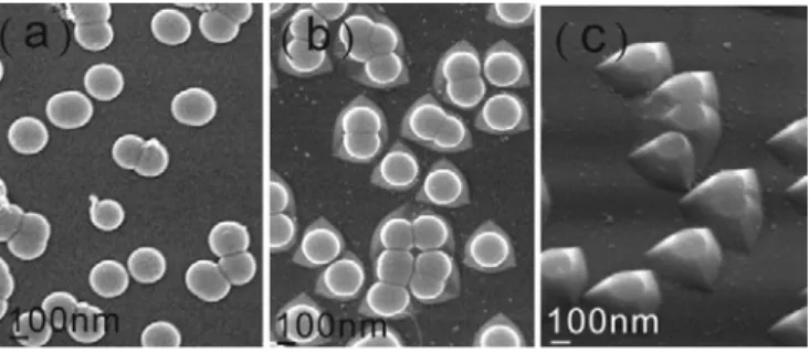
The SEM images of as-deposited LPD-SiO2and NPSS are
shown in Fig. 1. The LPD-SiO2 deposited on the sapphire
surface was in the shape of hemispheres having a diameter of 200–300 nm and a height of 100–150 nm. As shown in Fig. 1(a), the LPD-SiO2 was uniformly distributed on the
sapphire surface and the pattern coverage was about 45%.
HSIEH et al.: IMPROVEMENT OF EPITAXY GaN QUALITY 2233
Fig. 1. Plane-view SEM images of (a) as-deposited LPD-SiO2, (b) nano
patterns formed by wet etching process, and (c) side-view SEM image of nano patterns.
After the wet etching process, pyramid-shapednano patterns having a diameter of 250–300 nm and a height of 200–300 nm were formed, as shown in Fig. 1(b) and (c). The appearance of these pyramid-shaped nano patterns is similar to that of micron patterns in Ref. [2].
The GaN crystal quality was first analyzed by XRD rocking curves (XRCs), which show that the full-width at half-maximum (FWHM) of NPSS-GaN was less than that of FLAT-GaN. Compared with FLAT-GaN, NPSS-GaN had FWHM of (002) GaN decreased from 427.9 to 367.1 arcsec, and FWHM of (102) GaN reduced from 586.9 to 362.7 arcsec. These results indicate that the GaN crystallinity of NPSS-GaN was superior to that of FLAT-GaN.
In addition to XRCs, the CL method was also employed to evaluate the GaN crystal quality. Figure 2(a) is the cross-sectional SEM image of NPSS-GaN. It clearly shows voids around nano patterns and a fully coalesced GaN. The CL spectra were collected from the area near nano patterns (spot 1) and the middle of the GaN film (spot 2) in both samples. The spectra integral intensity of NPSS-GaN at spot 1 was 9.3×10⁴, which was 3.2 times higher than that of FLAT-GaN. As for spot 2, the integral intensity of NPSS-GaN was 2.2 × 10⁶, which was even 7.3 times higher than that of FLAT-GaN (3× 10⁵).
The improvement in structural quality of the middle region (spot 2) was verified by measuring the etching pit density (EPD). Samples were grinded till undoped GaN was revealed (∼ 2.5 µm from the GaN/sapphire interface), followed by etching samples in 270 °C H3PO4 for 3 minutes. The EPD
of NPSS-GaN was 2.7 × 106cm−2, which was much lower than that of FLAT-GaN, 3.3×107cm−2. These results indicate that the GaN crystallinity of NPSS-GaN was superior to that of FLAT-GaN in the middle region.
TEM was also employed to investigate the crystal quality of NPSS-GaN. As shown in Fig. 3, voids were found at the corner of nano patterns. Dislocations originated from the GaN/sapphire interface due to the large lattice misfit. Lots of dislocations then extended to the upper region. However, around the nano-patterned regime, with increase in growth time, GaN epilayers on the c-plane sapphire covered these nano patterns with lateral growth, thus causing the threading dislocation to bend towards the patterns, or end at the GaN/void interfaces [17]–[19]. Therefore, not many disloca-tions were found on the top of the nano patterns.
Fig. 2. (a) Cross-sectional SEM image of NPSS-GaN. (b) CL spectra of NPSS-GaN and FLAT-GaN from spot 2.
Fig. 3. (a) Cross-sectional bright-field TEM image of GaN grown on NPSS. (b) and (c) High-magnification images of Fig. 3(a).
These TEM images clearly explain the CL observations. As shown in Fig. 3, most of the growth of GaN was initiated from the c-plane instead of the LPD-SiO2 surface Compared
with FLAT-GaN, NPSS has less area to initiate GaN, thus reducing the total GaN defect density at spot 1. These results are similar to the conclusions drawn by Ref. [12] in their GaN growth studies. The total defect density (EPD) was reduced from 4.31 × 10⁷ to 0.52 × 107cm−2 when the c-plane-area ratio decreased from 59.6% to 9.6%. Therefore, NPSS-GaN had higher CL intensity than FLAT-GaN at spot 1.
As for spot 2, since the dislocations bend towards the patterns, or end at the GaN/void interfaces, NPSS-GaN has much higher CL intensity than FLAT-GaN.
2234 IEEE PHOTONICS TECHNOLOGY LETTERS, VOL. 24, NO. 24, DECEMBER 15, 2012
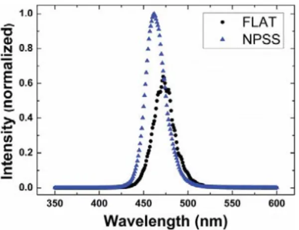
Fig. 4. Photoluminescence of multiple quantum wells grown on NPSS and FLAT sapphire.
PL was employed to investigate the quality of multiple quantum wells (MQWs) shown in Fig. 4. The excitation source was a 325-nm, 30-mW He-Cd continuous wave laser. The slight shift in PL peaks might be due to the same growth conditions of both samples. The conditions should be different since these two substrates have different surface morphologies. However, in order to reduce the experimental variables, same growth conditions were used in this letter. The PL peak intensity of MQWs grown on NPSS is 1.5 times higher than that grown on FLAT. This observation suggested that with threading dislocations bending toward the nano patterns at lower regions, NPSS can efficiently enhance the quality of MQWs by improving the crystal quality at the upper region.
IV. CONCLUSION
In this letter, a maskless and relatively simple LPD method was employed to deposit nanoscale SiO2 hemispheres on
sapphire substrates. Then, LPD-deposited sapphire was etched in a 3H2SO4:1H3PO4 mixed solution to fabricate NPSS. The
GaN films were fully coalesced and voids can be found on the corners of nano patterns. The XRCs, EPD and monochro-mated CL maps show that NPSS-GaN has better quality than FLAT-GaN. TEM analysis reveals that GaN was initiated from the c-plane instead of the LPD-SiO2surface. Moreover, lots of
dislocation on NPSS-GaN bend toward the patterns, or end at the GaN/void interfaces. As a result, the defect density in the middle region of NPSS-GaN was further reduced. The MQWs grown on NPSS show PL peak intensity of 1.5 times higher than that on FLAT.
ACKNOWLEDGMENT
The authors would like to thank the National Nano Device Laboratory, Taipei, Taiwan, the Center for Nanoscience and Technology, Notre Dame, IN, the Nano Facility Center, Minneapolis, MN, and the Semiconductor Laser Technology Laboratory of the National Chiao Tung University, Hsinchu, Taiwan, for technical support.
REFERENCES
[1] K. Tadatomo, et al., “High output power InGaN ultraviolet light-emitting diodes fabricated on patterned substrates using metalorganic vapor phase epitaxy,” Phys. Status Solidi A, vol. 188, no. 1, pp. 121–125, 2008.
[2] B. W. Lin, C. Y. Hsieh, B. M. Wang, W. C. Hsu, and Y. C. S. Wu, “Improved performance of GaN-based LEDs by covering top C-plane of patterned sapphire substrate with oxide layer,” Electrochem.
Solid-State Lett., vol. 14, no. 8, pp. J48–J50, 2011.
[3] P. Kumar, A. Khanna, S. Y. Son, J. S. Lee, and R. K. Singh, “Analysis of light out-coupling from microlens array,” Opt. Commun., vol. 284, no. 19, pp. 4279–4282, 2011.
[4] H. Gao, F. Yan, Y. Zhang, J. Li, and Y. Zeng, “Enhancement of the light output power of InGaN/GaN light-emitting diodes grown on pyramidal patterned sapphire substrates in the micro- and nanoscale,” J. Appl.
Phys., vol. 103, no. 1, pp. 014314-1–014314-5, 2008.
[5] W. Cao, J. M. Biser, Y. K. Ee, X. H. Li, and N. Tansu, “Dislocation structure of GaN films grown on planar and nano-patterned sapphire,”
J. Appl. Phys., vol. 110, no. 5, pp. 053505-1–053505-4, 2011.
[6] H. W. Huang, J. K. Huang, S. Y. Kuo, K. Y. Lee, and H. C. Kuo, “High extraction efficiency GaN-based light-emitting diodes on embedded SiO2nanorod array and nanoscale patterned sapphire substrate,” Appl.
Phys. Lett., vol. 96, no. 26, pp. 263115-1–263115-3, 2010.
[7] Y. Li, et al., “Defect-reduced green GaInN/GaN light-emitting diode on nanopatterned sapphire,” Appl. Phys. Lett., vol. 98, no. 15, pp. 151102-1–151102-3, 2011.
[8] Y. S. Lin and J. A. Yeh, “GaN-based light-emitting diodes grown on nanoscale patterned sapphire substrates with void-embedded cortex-like nanostructures,” Appl. Phys. Express, vol. 4, no. 9, pp. 092103-1–092103-3, 2011.
[9] D. H. Kim, U. Farva, W. S. Jung, E. J. Kim, and C. H. Park, “GaN epitaxial layers grown by the solution-cast seed layer HVPE technique: Effect of reactor heating method on structural and optical quality,” Mater.
Lett., vol. 62, nos. 12–13, pp. 1859–1862, 2008.
[10] D. H. Kim, U. Farva, W. S. Jung, E. J. Kim, and C. H. Park, “Epitaxial growth of GaN on (0001) Al2O3via solution-cast seed layer formation
process using Ga(mDTC)3,” Korean J. Chem. Eng., vol. 25, no. 5, pp.
1184–1189, 2008.
[11] M. K. Lee, C. L. Ho, and C. H. Fan, “High light extraction efficiency of gallium nitride light emitting diode with silicon oxide hemispherical microlens,” Appl. Phys. Lett., vol. 92, no. 6, pp. 061103-1–061103-3, 2008.
[12] M. K. Lee, C. L. Ho, and C. H. Fan, “Enhancement of light extraction efficiency of gallium nitride flip-chip light-emitting diode with silicon oxide hemispherical microlens on its back,” IEEE Photon. Technol. Lett., vol. 20, no. 15, pp. 1293–1295, Aug. 1, 2011.
[13] J. S. Chou and S. C. Lee, “The initial growth mechanism of silicon oxide by liquid-phase deposition,” J. Electrochem. Soc., vol. 141, no. 11, pp. 3214–3218, 1994.
[14] C. S. Lai, T. F. Lei, and C. L. Lee, “The electrical characteristics of polysilicon oxide grown in pure N2O,” IEEE Electron Device Lett.,
vol. 16, no. 9, pp. 385–386, Sep. 1995.
[15] C. J. Huang, M. P. Houng, Y. H. Wang, N. F. Wang, and J. R. Chen, “Improved formation of silicon dioxide films in liquid phase deposition,”
J. Vac. Sci. Techno. A, Vac. Surf. Films, vol. 16, no. 4, pp. 2646–2652,
Jul. 1998.
[16] H. Nagayama, H. Honda, and H. Kawahara, “A new process for silica coating,” J. Electrochem. Soc., vol. 138, no. 8, pp. 2013–2016, 1988. [17] J. H. Cheng, Y. C. S. Wu, W. C. Liao, and B. W. Lin, “Improved
crystal quality and performance of GaN-based light-emitting diodes by decreasing the slanted angle of patterned sapphire,” Appl. Phys. Lett., vol. 96, no. 5, pp. 051109-1–051109-3, 2010.
[18] W. K. Wang, et al., “Near-ultraviolet InGaN/GaN light-emitting diodes grown on patterned sapphire substrates,” Jpn. J. Appl. Phys., vol. 44, no. 4B, pp. 2512–2515, 2005.
[19] C. H. Chiu, et al., “High efficiency GaN-based light-emitting diodes with embedded air voids/SiO2 nanomasks,” Nanotechnology, vol. 23,