Illumination system for wire bonding inspection
Der-Baau Perng, Cheng-Chuan Chou, and Shu-Ming Lee
A novel lighting system was devised for 3D defect inspection in the wire bonding process. Gold wires of 20m in diameter were bonded to connect the integrated circuit (IC) chip with the substrate. Bonding wire defects can be classified as 2D type and 3D type. The 2D-type defects include missed, shifted, or shorted wires. These defects can be inspected from a 2D top-view image of the wire. The 3D-type bonding wire defects are sagging wires, and are difficult to inspect from a 2D top-view image. A structured lighting system was designed and developed to facilitate all 2D-type and 3D-type defect inspection. The devised lighting system can be programmed to turn the structured LEDs on or off independently. Experiments show that the devised illumination system is effective for wire bonding inspection and will be valuable for further applications. © 2007 Optical Society of America
OCIS codes: 120.4630, 150.3040.
1. Introduction
Wire bonding is a very important process in wafer packaging. The accuracy of this process will determine the packaging quality of the final product. Every single unit (chip) sawed from a wafer manufactured by a semiconductor company is sent for bonding before packaging. The bonding machine picks up one chip and places it onto the substrate and then links the bond pad to its corresponding lead using the gold wire con-tinuously. After the wire bonding process, the dam glob process is continued to protect the chip and the wire from damage. Figure 1 illustrates part of a wire bonded integrated circuit (IC) on the substrate.
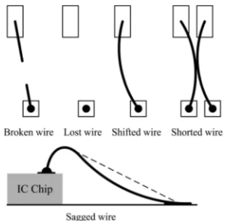
The minimum diameter of a bonding wire, which appears as a 3D loop in an IC chip, is approximately 20m. This kind of bonding wire easily bends or sags in the middle segment. Figures 2 and 3 illustrate a good wire and possible defects of the bonding wire. Possible bonding wire defects can be classified into 2D and 3D defect types. A 2D-type defect could be inspected by using a single 2D image from the top view. The objective of 2D-type defect inspection is to detect whether any wire is missing, shifted, or
shorted. The 3D-type defect indicates that the 3D features of a wire, such as the height, have to be inspected. Some wire defects such as broken or lifted wires, though technically height defects, can still be inspected by using a single 2D image. In this paper a major 3D-type defect to be inspected is wire sagging, which cannot be inspected using a 2D image. A 3D sagging in the bonding wire is caused by gravity or other forces. Bonding wire sagging will reduce wire strength and must be detected. A sagging wire will usually appear to be a good wire when captured in a 2D image. More information has to be provided or extracted for inspection. Currently, the quality of wires bonded on an IC is checked by human inspec-tors with microscopes. This process is inefficient, and it is hard for the human eye to identify the actual defective location of bonding wires on all IC chips. Because of this, an automatic optical inspection (AOI) system is required to help check chip bonding wires. This study has developed an AOI system for inspect-ing bondinspect-ing wires.1
Because of the tiny diameter and 3D loop of the bonding wire, IC inspection requires a well-designed lighting system that will illuminate the bonding wires more than the background. Bonding wire illu-mination requirements were achieved by deriving the reflection model of the bonding wires. A new struc-tured LED lighting system was then developed that will provide suitable illumination for general bonding wire inspection, especially for 3D-type sagging wire defect inspection.
This paper is organized as follows. In Section 2, related research and lighting device surveys are pre-sented. Bonding wire reflection models are described
The authors are with the Department of Industrial Engineer-ing and Management, National Chiao-Tung University, 1001 Ta Hsueh Road, Hsinchu 30050, Taiwan. D.-B. Perng’s e-mail address is [email protected].
Received 15 June 2006; revised 18 October 2006; accepted 18 October 2006; posted 20 October 2006 (Doc. ID 71958); published 2 February 2007.
0003-6935/07/060845-10$15.00/0 © 2007 Optical Society of America
in Section 3. In Section 4, a structured lighting sys-tem is proposed for wire bonding inspection. Conclu-sions are given in Section 5.
2. Literature Review A. Related Research
The bonding ball and bonding wire are the two pri-mary factors in wire bonding inspection. Zhang et al.2 developed a visual inspection system for measuring bonding ball height by using a structured lighting technique. This light source is an incandescent lamp that is focused twice, through a slit, to form a narrow stripe. The stripe is set at an angle of 45° to measure the height of the bonding ball from the pad plane. Lim et al.3developed a system for bonding ball in-spection. Bonding ball height was detected by au-tomatically computing the focused planes of both the top and the base of the bonding ball by using a series of 2D images. Currently, bonding machines are precise enough to produce bonding balls with very good height, and so industry focus has shifted to bonding wire inspection.
King and Sing4presented an algorithm for inspect-ing bondinspect-ing wires. They used a Hough transforma-tion to determine the straight-line equatransforma-tion of the bonding wire. A fiber-optic ring light was used as the light source to highlight the bonding wires. Ye et al.5 presented an inspection system that applied a stereo
vision technique to detect defects related to the 3D profile of bonding wires. They proposed that the illu-mination system should maximize light reflected from the bonding wires and should minimize light reflected from the surface of the chip or the back-ground of the bonding wires. An optical fiber with a ring head was used to provide side-light illumination. The emitted side light is almost parallel to the chip surface, with an angle lower than 15°.
To detect 3D-type bonding wire defects from a sin-gle 2D image, the illumination system should provide 3D bonding wire information in a 2D image. Some researchers used structured light for illumination. The 3D shape of the bonding wires was reconstructed by using features from its 2D image. Wang and Cheng6used a slide projector as the illumination to project a grid pattern onto the object’s surfaces. Woodham7proposed a photometric method to recover the surface orientation unambiguously. Some other researchers8 –10 recovered the 3D shape by using a photometric method and a structured lighting sys-tem. However, these studies require multi-images in order to determine normal surfaces.
B. Lighting Source Surveys
A good review of lighting system design complete with guidelines and illustrations can be found in Bachelor.11Following that, we have used three light-ing devices for bondlight-ing wire inspection: circular flu-orescent, dome-type LED, and linear inclined optical fiber.12 The incident light angle and its effective spread range are the two critical factors in lighting device design.
1. Circular Fluorescent Light
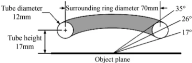
The circular fluorescent light can provide surround-ing light in varysurround-ing incident angles by controllsurround-ing its setup height. An illustration of a circular fluorescent lighting device is given in Fig. 4.
2. Dome-Type LED
The dome-type LED can provide surrounding light in a large spread range of incident angle as shown in Fig. 5.
Fig. 3. Five possible bonding wire defects.
Fig. 1. (a) Illustrative image and (b) enlarged top view of part of a wire bonded IC.
3. Linear Inclined Optical Fiber
The linear inclined optical fiber can provide light in a controllable incident angle and spread range as shown in Fig. 6.
By using three lighting devices in this study, many bonding wire images were captured; they are sum-marized in Table 1. The lighting devices were set up in experiential proper positions to achieve optimal illumination. The second column of Table 1 shows three images for 2D wire inspection. The images rep-resent the location of wires clearly, and all three lighting devices can illuminate the bonding wire for 2D inspection. Figure 7 shows the histogram of the captured image using linear inclined optical fiber. The gray value of the background in Fig. 7 is very low and easily distinguishable, that is, the wire can be separated from the captured image by using the bi-nary method with a predefined threshold, such as 128.
The third column of Table 1 shows captured images for 3D wire inspection. An intentionally sagging wire was tested by 3D wire inspection. Of the three types of lighting devices, the captured images show that only the linear inclined optical fiber can highlight the 3D sagging defect. The sagging is represented as a gap in the 2D image captured by using the linear inclined optical fiber, and it is obvious by inspection. The surrounding light of the circular and dome-type lighting devices erases the sagging feature, and these cannot be used for 3D wire inspection. This paper presents a simplified bonding wire reflection model and what is believed to be a novel lighting system for bonding wire inspection.
3. Bonding Wire Reflection Model
Because an image of bonding wires is formed by fea-tures reflected from both the background and the wires, the pseudosurface orientation formed by the
bonding wires will affect the reflection on the image. The bonding wire features can then be extracted from the captured image. In Woodham’s research,7at least three images were required to derive the surface ori-entation of the reflected object. This paper proposes a simplified bonding wire reflection model and a proper lighting system for capturing the wire’s clear image. Using the developed lighting system, an AOI system can extract and detect possible bonding wire defects using only one top-view 2D image.
The simplified bonding wire reflection model is shown in Fig. 8. The critical segment of each wire is simplified as a straight line. The incident angle of the
Fig. 6. Linear inclined optical fiber.
Table 1. Illumination of the Effect Using the Circular Fluorescent, the Dome-Type LED, and the Linear Inclined Optical Fiber
Captured Image Lighting Device For 2D Wire Inspection For 3D Wire Inspection Circular fluorescent Dome-type LED Linear inclined optical fiber Fig. 4. Incident angle of a circular fluorescent light with
sur-rounding ring diameter of 70 mm and tube height of 17 mm. The incident light angle ranges from 17° to 35°.
light () and the inclined slope of the reflective sur-face 共兲 are the two variables to be considered. The relationship between and can be derived as
⫽4 ⫺2. (1) That is, the inclined slope of the bonding wire reflec-tive surface can be derived from a CCD-captured
im-age. Assume G共x, y兲 is the gray level of a pixel in the image, which corresponds to a point共x, y兲 on the re-flective surface of the bonding wire. When the inci-dent light angle is set as and the gray value G共x, y兲 is greater than that of background, then the angle between the reflective surface and the horizontal sur-face is.
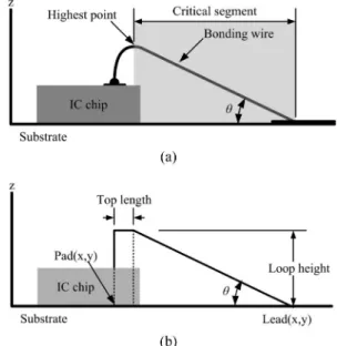
The computer-aided design (CAD) file of bonding wires records calibration mark coordinates on the substrate and the IC chip, the starting point (pad), and the ending point (lead) of each of the bonding wires. A bonding machine first searches for a calibra-tion mark, makes some adjustments, and then bonds gold wires to connect the IC chip with the substrate. When one end of a bonding wire is formed as a bond-ing ball and is stuck onto a pad, the bondbond-ing machine capillary will guide the bonding wire to its corre-sponding lead on the substrate. The capillary makes
the bonding wire hit and connect to the lead, and cuts off the bonding wire at the same time. The factors related to the bonding wire are the pad and lead coordinates, the loop height, and the top length. An actual bonding wire loop is shown in Fig. 9(a). An illustration of the capillary track is shown in Fig. 9(b). In this bonding process, every wire is bonded to a similar slope from the highest point to its correspond-ing lead. In some cases the bondcorrespond-ing machine may make one or two bends in a longer bonding wire to enhance its strength. Generally, each bonding wire in between two adjacent bends has a similar slope. For wire inspection it is necessary to have a clear image of the wire so that the captured wire image can be compared to the given electronic CAD file. To avoid reflection interference caused by the substrate back-ground, only the critical segment of the bonding wire, from the highest point to the lead, is captured and inspected. The AOI system can get these factors from the bonding machine to calculate the slope of the wire. The relationship of the wire slope, the pad and lead coordinates, the loop height and the top length can be represented by
Once the slope of the bonding wire is given, the light-ing device can be set up at a proper incident angle to illuminate the bonding wire.
The bonding wire loop may be affected by gravity or may be damaged by other forces. For a wire that has
⫽ tan⫺1
冉
Loop height冑
共Pad共x兲 ⫺ Lead共x兲兲2⫹ 共Pad共y兲 ⫺ Lead共y兲兲2⫺ Top length冊
. (2) Fig. 7. Captured image histogram for the linear inclined opticalfiber.
Fig. 9. (a) Bonding machine capillary track, (b) side-view illus-tration of an 3D actual loop of a bonding wire-connecting the pad and lead.
a slope of 20°, for example, the incident angle of light should be at 50° to make a good reflection, by Eq. (1). Using the captured image, it is possible to detect the location of the bonding wire with a developed AOI system. This is because the bonding wires are ar-ranged surrounding the four sides of a chip, and the bonding wires along each side of the chip form a pseudoreflective surface. An independent light source is needed, as shown in Fig. 10, which can illuminate each of the four reflective surfaces. In this case, the designed lighting device should provide sufficient light to illuminate the bonding wires clearly in each captured image.
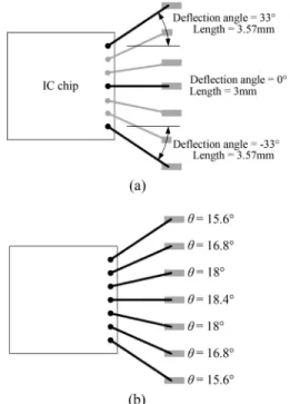
Another reflection model issue is the bonding wire layout. Both the pads and the leads are arranged along the four boundary edges of an IC chip. Because the interval of adjacent pads is smaller than that of the leads, the bonding wire layout on one side of the IC chip has to be set in a fan shape, as shown in Fig. 11(a). The bonding wire located in the middle has no deflection angle, while the wire closest to the corner of the IC chip has the largest deflection angle and span. As each wire is bonded at the same height, the bonding wire located closest to the corner of the IC chip is longer and has a smaller slope than the wires located in the middle. For example, a 1 mm high bonding wire with a 0° deflection angle and a length of 3 mm has a slope of 18.4° (inclined slope ⫽ tan⫺1共highest point兾length兲). In comparison, a 1 mm high bonding wire with a 33° deflection angle and a length of 3.57 mm has a slope of only 15.6° as illus-trated in Fig. 11(b). To clearly highlight bonding wires with different slopes or deflection angles, a lighting device must be able to provide light at dif-ferent incident angles from difdif-ferent directions.
To simplify the bonding wire reflection model, the critical segment of each bonding wire is approxi-mated as a straight line segment. A pseudoreflective surface is a wire surface formed by linking all the highest points of the critical segments, the left-most and the right-most bonding wire, and the associated leads in one side of an IC chip as shown in Fig. 12. For a bonding wire with a deflection angle of 0°, only the part closest to and on the same side as the light source will reflect the light into the CCD. Once the
wire surface is illuminated all the bonding wires in this surface can be located in the captured image. The height and the projected length of the wire surface will decide the incident angle, i.e., the slopewire surface, between the pseudo-wire-surface and the substrate. Thewire surfaceis approximately equal to the slope of the bonding wire with a deflection angle of 0°. The slope of a pseudoreflective surface can be represented as
wire surface⫽ tan⫺1
冉
height of wire surface projective length of wire surface
冊
.(3)
If the lighting device is set at the incident angle ac-cording to Eqs. (1) and (3), all the bonding wires lying on the pseudoreflective surface of the bonding wires can reflect the highest intensity into the CCD.
For 2D-type defect inspection, it is necessary to illuminate and capture the critical segment first. Practically, a slight slope variance of the critical seg-ment is not treated as a defect, that is, the lighting
Fig. 10. Four independent light sources. Each is designed to il-luminate one of the four pseudoreflective surfaces formed by IC chip bonding wires.
Fig. 11. Bonding wires located along one side of an IC chip with (a) different deflection angles and (b) different slopes.
Fig. 12. Stereograph of a pseudoreflective surface formed by the bonding wires on one side of an IC chip.
device should be designed to illuminate the critical segments of bonding wires at an allowable variance. For example, a pseudo-wire-surface has a slope wire surface at 20°, and the maximum allowable vari-ance of the slope is⫾5° (the slope of each of the good wires ranges from 15° to 25°). The spread range of incident light angle should cover 40°– 60° to illumi-nate the wire according to Eq. (1).
For 3D-type defect inspection, the incident light angle should be spread in an exact range to illumi-nate the good wires and to highlight the sagging wires at the same time. To illustrate slope variance, the lighting device should provide light in a control-lable spread range of incident angle. For example, if the lighting device can provide light with an incident angle of 4°, it can illuminate a wire at a slope of 2°. Sagging in the range of ⫾1° can be highlighted for inspection. Since the profile of a bonding wire is a 2D curve, some unexpected reflection and scattering may exist with a surrounding light source. For 3D wire inspection, the light source should provide suitable light to highlight the bonding wires at each of the four sides of an IC chip simultaneously without causing any unexpected scattering.
4. Structured LED Lighting System for Bonding Wire Inspection
Since no available lighting device fully satisfied the needs of the bonding wire inspection, a structured lighting system for 2D- and 3D-type defect inspection was developed and is presented in this section. A. Concept and Prototype of the Structured LED Lighting System
In 2D-type defect inspection, the light source must provide light with a proper incident angle and large spread range to suitably illuminate bonding wires.1In 3D-type defect inspection the lighting device should provide light with an exact spread of incident angle so that sagging wires can easily be distinguished from good wires.
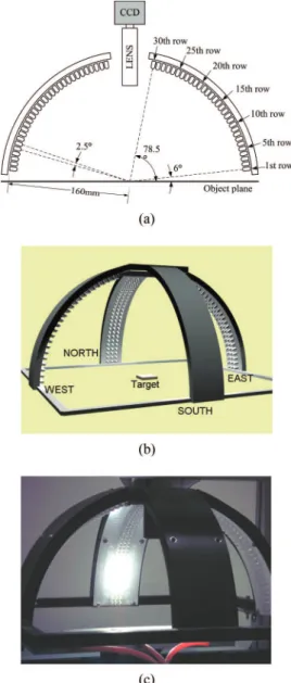
To provide suitable light with a controllable inci-dent angle and spread range for each of the four sides of an IC chip without mechanism movement, we de-signed a prototype structured lighting system con-taining four LED arrays for this objective. Each LED array was mounted on a soft printed circuit board. The four soft printed circuit boards were fixed sym-metrically at the north, south, east, and west strips of a hemispheric holder, as shown in Fig. 13. This configuration matches the four LED arrays with the bonding wires at the four sides of an IC chip. LEDs on different rows can be programmed to turn on or off independently, that is, both the incident light angle and the spread range of the incident light can be totally controlled electronically, highlighting the bonding wires without any mechanical movement. Ac-cording to Eq. (1), light with a smaller controllable spread range of incident angle can distinguish a slight sagging defect. Both the smaller LED and the larger working distance result in a smaller spread range of incident light angle. In the developed prototype, each
LED array contains 30 rows of LEDs, and the working distance is set at 160 mm so that each LED row can provide a fixed 2.5° spread range of incident light. Fol-lowing Eq. (1), each row of LEDs in the prototype can illuminate bonding wire with a slope in the range of 1.25°. The lowest row is set to provide light at a 6° incident angle, so that this row of LEDs is a little higher than the highest bonding wire to avoid collision. The proper number of LEDs on each row can be pro-grammed to provide sufficient light without unex-pected reflection to the CCD. When the LEDs mounted on the ith to jth rows are turned on, the range of slope of the illuminated bonding wire can be calculated by using Eq. (4). For example, the LEDs on the fifth to eighth rows can illuminate the bonding wires with slopes from 3258° to 3758°:
Fig. 13. (Color online) (a) Side view of the proposed structured lighting system. For clarity, only the east and west strips of LED arrays and associated soft PCBs are depicted. (b) 3D illustration of the structured lighting system. (c) Photograph of the prototype of the proposed structured LED lighting system.
90⫺ upper boundary of incident light angle
2 ,
⬍inclined slope of illuminated bonding wire ⬍90⫺ lower boundary of incident light angle2 , That is,
90⫺关6 ⫹ 共 j ⫺ 1兲 * 2.5 ⫺ 1.25兴
2 .
⬍inclined slope of illuminated bonding wire ⬍90⫺关6 ⫹ 共i ⫺ 1兲 * 2.5 ⫺ 1.25兴2 . (4) B. Illumination Effect of the Structured LED Lighting System
In Subsection 2.B, three types of lighting device were tested for 2D and 3D bonding wire inspection. In this section illumination results of the structured LED lighting system will be presented. In Subsection 4.B.1, the structured LED lighting system was set to provide light with a proper incident angle and spread range to illuminate the bonding wires on one side of the IC chip for 2D wire inspection. In Subsection 4.B.2, the structured LED lighting system was tested for 3D wire inspection. Three IC chips with good, slightly sagging, and seriously sagging bonding wires were used as test samples. These IC chips were spe-cially made, and only one wire was bonded in one edge for easily capturing the profile of the bonding wires. The structured LED lighting system was set to provide light with a proper incident angle and spread range to distinguish the good, slightly sagging, and seriously sagging bonding wires.
1. Illumination Effect for 2D-Type Defect Inspection
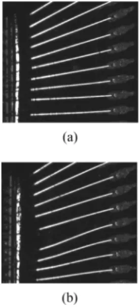
When the bonding wire surface slope was obtained from the CAD data, the LEDs on proper rows were turned on, according to Eq. (3), to provide good illu-mination. For example, the slope of the bonding wire surface of the 2D sample IC is 32° as shown in Fig. 14. The proper incident light angle should be 26°, and the LEDs on the 5th to the 13th rows of the developed structured lighting system were turned on. These LEDs projected light in incident angles from 17.25° to 34.75° onto the wires. According to Eq. (4), all the bonding wires spread in the range from 2758° to 3638° will be clearly highlighted, and 2D-type defects and their locations can easily be found from captured images, that is, the structured LED lighting system can illuminate the bonding wires clearly.
2. Illumination Effect for 3D-Type Defect Inspection
According to Eq. (1), each row of the structured LED lighting system with an incident angle can
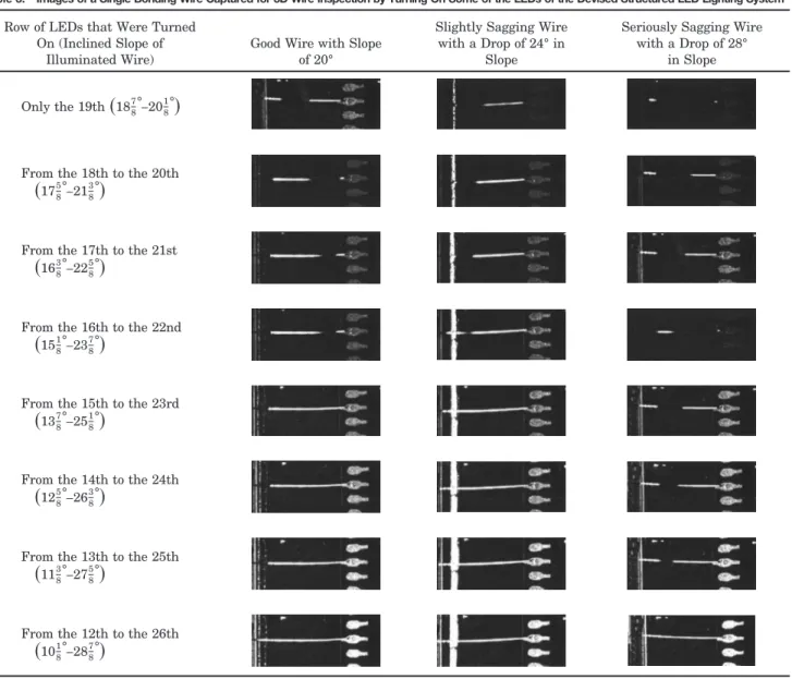
illumi-nate bonding wires with a corresponding slope of. Figure 15 shows the profile of a good bonding wire and Table 2 shows the images captured by using the structured LED lighting system. First, only one row of the structured LED lighting system was turned on and then more rows were turned on to provide the best illumination. For clarity, images can be omitted that have no bonding wire captured when the LEDs on the 1st to the 12th rows and the 22nd to the 30th rows were turned on. When the LEDs on the 16th to 19th rows were turned on simultaneously, the entire critical segment of the bonding wire was illuminated perfectly.
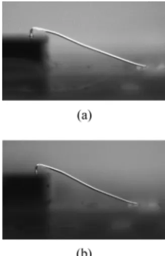
For 3D-type defect inspection, the developed LED lighting system must provide light with any desired spread range of incident angle to distinguish sagging wires from good wires. The good bonding wire sample in this experiment was deflected away from the mid-dle wire approximately 20°. A serious drop was found in the critical segment of one sample wire with an inclined slope of 28°, while a slight drop was found in the other critical segment of the wire with a slope of 24°, as shown in Fig. 16. Table 3 shows the captured images of a good wire and two sample bonding wires under different spread ranges of incident light angle. The LEDs on the 19th row were set as the center of the incident light angle, and the spread range of the incident light angle increased gradually. For the good wire, when the LEDs on the 16th to the 22nd rows were turned on, the whole critical segment was
illu-Fig. 14. Image of bonding wires captured using the structured LED lighting system. (a) All good wires, (b) some shifted wires.
minated clearly. With the same setting, both the slightly and the seriously sagging wires were repre-sented as a broken line in the captured image, that is, both the slightly and the seriously sagging wires can be detected using this setting.
When the LEDs on the 15th to 23rd rows were turned on, the slightly sagging wires were repre-sented as a continuous line, but the seriously sagging wires still looked like a broken line in the captured image, that is, only seriously sagging wires can be detected using this setting. From these experiments we can see that the devised structured LED lighting system can distinguish sagging defects in different degrees by controlling the spread range of the inci-dent light angle. This makes it easy for the AOI sys-tem to detect 3D-type sagging defects with various inspection specifications.
3. Image Capturing Process Using the Structured LED Lighting System
Because the spread range of the incident light angle of the structured LED lighting system is programma-ble, it can be used to highlight variant IC chips. Even if wire surfaces on all four sides of an IC chip have different inclined slopes the AOI system can turn on the proper rows and strips of the proposed lighting system after calculating the inclined slope of the wire surface. With this lighting system, the AOI system can successfully filter out all 3D-type defects by using only a single 2D top-view image. The algorithm for capturing the bonding wire images of an IC is de-scribed below.
Algorithm of bonding wire image capturing. Input: an electronic CAD data file of the bonding
wire, an IC chip with bonded wires,
Output: four images of each of the four-sided
bond-ing wire of this IC chip.
Procedure:
Move the IC chip to the initial position of the AOI system,
For i⫽ 1 to 4 do Table 2. Images of a Single Bonding Wire Captured by Turning on
Some of the LEDs of the Developed Structured LED Lighting System
Turned on LEDs
Inclined Slope of
Illuminated Wire Captured Image
13th 2638°–2758° 14th 2518°–2638° 15th 237 8°–25 1 8 ° 16th 2258°–2378° 17th 2138°–2258° 18th 201 8°–21 3 8 ° 19th 1878°–2018° 20th 1758°–1878° 21st 1638°–1758° From 16th to 19th 1878°–2378°
Fig. 16. Profiles of the slightly sagging wires with a drop of 24° in slope and seriously sagging wires with a drop of 28° in slope.
Calculate the inclined slope of the pseudo-wire-surface in side (i) of the IC chip from the input CAD file, according to Eq. (3),
(Note: Side (1), side (2), side (3), and side (4) correspond to the bonding wires in each of the four sides of the IC chip.)
Calculate the number of rows of LEDs, which will correspond to side (i) according to Eq. (1), Turn on the LEDs of the proper rows for provid-ing good illumination of the pseudo-wire-surface of side (i),
Capture a serial image of the bonding wires in side (i) of the IC chip,
Merge these images of the bonding wires of side (i) of the IC chip as the image (i).
End for End procedure
After image capturing, the algorithms developed by Perng et al.1can be used to inspect the bonding wire defects after slight modification, and 2D- and
3D-type defects can then be inspected from only one 2D image by using the devised structured LED lighting system.
5. Conclusions
Bonding wire defects are difficult to inspect without feasible lighting. No available lighting device can sat-isfy the 3D-type bonding wire defect inspection re-quirements. A novel structured LED lighting system has been developed in this paper. The devised struc-tured LED lighting system contains four LED arrays and can be programmed to illuminate critical seg-ments of bonding wires for 2D defect inspection and to highlight the sagging part of bonding wire for 3D-type defect inspection. With the aid of this structured LED lighting system and the proposed inspection algo-rithms, experiments show that the 2D- and 3D-type bonding wire defects can be successfully detected in a very efficient and effective way from a single 2D image. The devised structured lighting system can also be applied to the inspection of other similar objects, such
Table 3. Images of a Single Bonding Wire Captured for 3D Wire Inspection by Turning On Some of the LEDs of the Devised Structured LED Lighting System
Row of LEDs that Were Turned On (Inclined Slope of
Illuminated Wire)
Good Wire with Slope of 20°
Slightly Sagging Wire with a Drop of 24° in
Slope
Seriously Sagging Wire with a Drop of 28°
in Slope
Only the 19th
共
1878°–2018°兲
From the 18th to the 20th共
1758°–2138°兲
From the 17th to the 21st
共
1638°–2258°兲
From the 16th to the 22nd
共
1518°–2378°兲
From the 15th to the 23rd
共
1378°–2518°兲
From the 14th to the 24th
共
1258°–2638°兲
From the 13th to the 25th
共
1138°–2758°兲
From the 12th to the 26th
as the leads of quad flat packaged IC chips and the socket and slot connectors.
This work was partly supported by the National Science Council, Taiwan, under contracts NSC 93-2213-E-009-038 and NSC 94-2213-E-009-081.
References
1. D. B. Perng, C. C. Chou, and S. M. Lee, “A new wire bonding inspection system by machine vision,” Int. J. Adv. Manuf. Technol. (to be published).
2. W. Zhang, L. M. Koh, and E. M. C. Wong, “Computer vision system for the measurement of IC wire-bond height,” in IEEE Region 10 Conference on Computer, Communication, Control and Power Engineering (IEEE, 1993), pp. 948 –951.
3. H. O. Lim, W. Zhang, and L. M. Koh, “Automated visual in-spection for IC wire-bond using auto-focusing technique,” in 15th IEEE兾CHMT International Electronic Manufacturing Technology Symposium (IEEE, 1993), pp. 31–36.
4. N. N. King and B. K. Sing, “Automated inspection of IC bond-ing wires usbond-ing Hough transform,” in Proceedbond-ings of the 14th Annual Conference of Industrial Electronics Society (IEEE, 1988), pp. 844 – 847.
5. Q. Z. Ye, S. H. Ong, and X. Han, “A stereo vision system for the
inspection of IC bonding wires,” Int. J. Imaging Syst. Technol.
11, 254 –262 (2000).
6. Y. F. Wang and D. I. Cheng, “3-D shape construction and recognition by fusing intensity and structured lighting,” in Proceedings of IEEE International Conference on Systems, Man, and Cybernetics (IEEE, 1991), pp. 825– 830.
7. R. J. Woodham, “Photometric method for determining surface orientation from multiple images,” Opt. Eng. 19, 139 –144 (1980).
8. A. C. Sanderson, L. E. Weiss, and S. K. Nayar, “Structured highlight inspection of specular surfaces,” IEEE Trans. Pattern Anal. Mach. Intell. 10, 44 –55 (1988).
9. T. L. Chia, Z. Chen, and C. J. Yueh, “Curved surface reconstruc-tion using a simple structured light method,” in Proceedings of the 13th International Conference on Pattern Recognition (IEEE, 1996), pp. 674 – 678.
10. Y. L. Tian and H. T. Tsui, “3D shape recovery from two-color image sequences using a genetic algorithm,” in Proceedings of the 13th International Conference on Pattern Recognition (IEEE, 1996), pp. 938 –942.
11. B. G. Batchelor, “Lighting and viewing techniques,” in Auto-mated Visual Inspection, B. G. Batchelor, D. A. Hill, and D. C. Hodgson, eds. (Elsevier, 1985), pp. 103–179.
12. D. B. Perng, Department of IEM, National Chiao-Tung University, 1001 Ta Hsueh Road, Hsinchu, Taiwan 30050 (personal communication, 2004).