MICROELECTRONIC ENGINEERING
ELSEVIER Microelectronic Engineering 28 (1995) 101-104
Fabrication of MOSFETs Using Low-Temperature
Liquid-Phase Deposited Oxide
Ching-Fa Yeh, Shyue-Shyh Lin and Tzy-Yan Hong
Department of Electronic Engineering & Institute of Electronics National Chiao-Tung University, Hsinchu, Taiwan, ROC
Low-temperature, high quality liquid-phase deposition (LPD) oxide was developed. The MOSFETs with such a new LPD oxide as gate insulators were investigated. The electrical characteristics, including threshold voltage of 2.1 Volts, peak effective mobility (prs) of 580 cm2/V. s, and subthreshold swing of
134 mV/decade, show the devices exhibit comparable performance to other low-temperature processed MOSFETs. This demonstrates that LPD oxide can be an suitable candidate for future gate insulators in low-temperature processed MOSFETs.
I. INTRODUCTION
Current trends in scaled MOSFET fabrication have stimulated interested in low-temperature silicon processing [ l]-[5], because high-temperature processing may generate defects due to larger thermal stress. To date, a few MOSFET studies have looked at deposition of gate oxide at low temperatures [2]-[5], but they all needed expensive apparatus and complex processing to get high quality oxide film. Recently, a novel room-temperature liquid phase deposition (LPD) technique using inexpensive apparatus was developed for silicon oxide [6], [7]. The newest deposition mechanism of LPD oxide was proposed by authors [S] and briefly described as follows:
[SiF, x SiF412- + 4H20 +SiF4 + 2SiFh2- +Si(OH), + 2HF + 2H’ Si(OH)4 + Si(OH)4 -+ 2SiO2 + 4H20
According to this new mechanism, the key factors which will influence the reaction of LPD oxide were clarified. The high quality LPD oxide film may then be gotten by controlling these parameters in detail. Thus, we were interested in applying this low-temperature high quality LPD oxide to MOSFET gate insulators. This paper present the electrical characteristics of MOSFETs made with such a new LPD gate oxide, and compares them with those of other types of low-temperature processed MOSFETs.
II. EXPERIMENTAL
In the conventional deposition apparatus of LPD oxide, the polysilicic may form a spatial network in the solution and then precipitate on the surface. This phenomenon will make the LPD oxide more
roughness and less integrity. Thus, the new deposition apparatus, which can circulate and filter out particles to deposit high quality LPD oxide, was developed in this study, Figure 1 shows the schematic figure of this new apparatus.
N-channel MOSFETs with aluminum gates were fabricated on l-5 !&cm, (loo), p-type silicon substrates, A typical cross-sectional view of the fabricated device is shown in the inset of Fig. 2. The fabrication used conventional four-mask processes without channel implantation. The LPD oxide was first used as gate insulator. Specifics concerning the deposition process of LPD oxide were the same as those in our previous works [6][7], except the different deposition apparatus. Because the structure of LPD oxide
0167.9317/95/$09.50 D 1995 - Elsevier Science B.V. All rights reserved. SD1 0167-9317(95)00024-O
102 C. F. Yeh et al. / Microelectronic Engineering 28 (1995) 101-104
will change after treating at a temperature over 700°C [S], the processing temperature had to be carefully controlled to avoid affecting the LPD oxide. So in our MOSFET processes, thermal diffusion of phosphorus for the source and drain regions was adopted and performed before gate oxide deposition. In addition, we adopted an aluminum gate to replace the polycrystalline silicon gate, because aluminum evaporation has hardly any thermal effect on LPD oxide. Post-metal annealing at 400” C was the only high temperature process used after LPD oxide deposition.
III. RESULTS AND DISCUSSION
In order to investigate the advantage of new deposition apparatus, the LPD oxide deposited with new apparatus was characterized. Fig. 3 shows the surface inspection of LPD oxide with atomic force
microscope (AFM), we found that the LPD oxide had much smoother surface and no particles precipitated on the surface. And from the distribution of breakdown field, as shown in Fig. 4, we found that LPD oxide exhibited no low field breakdown. From above results, we may conclude that the film deposited uniformly and no weakspots existed in the film.
According to our new reaction equilibrium, we inferred that Hz0 added into the silica-saturated hydrofluosilicic acid (SSF) and the reaction temperature will majorly influence the reaction of deposition, i.e., the deposition rate. To investigate the influences of Hz0 added quantity and deposition temperature on the deposition rate of LPD oxide, different deposition conditions including Hz0 added quantity of 25 ml -
I50 ml in the SSF solution of 100 ml and deposition temperature of 5°C - 35“C was adopted. The results were shown in Fig. 5 and 6, respectively. The figure showed that the deposition rate increased linearly with Hz0 added quantity and exponentially increased with temperature. It reveals that the increment of reactant or reaction temperature would level up the reaction rate in the solution. In the same time, from the measurement results of refractive index, p-etch rate and electric field breakdown, we found that the better integrity of LPD oxide was formed at a lower deposition rate. According this, the LPD oxide with 30 nm thickness deposited at extremely low deposition rate was developed. Its I-V characteristics was shown in Fig. 7. From this figure, we may concluded that the LPD oxide deposited with new apparatus and best deposition conditions show comparable characteristics with other oxides. Thus, we were interested in applying this low-temperature LPD oxide to MOSFET gate insulator. In the same time, from the FTl.R spectrum, as shown in Fig. 8, the peak of 930 cm-’ was found. The peak in this position is Si-F bonds, indicating us that fluorine were incorporated in the LPD oxide film.
Fig. 9 shows the typical lo-V, characteristics of our MOSFET with Vo varied in the range from 2 V to 4 V in 0.5 V steps. The lo-VI, curve exhibiting triode characteristics and current saturation phenomena well, reveals a typical drain characteristics for a long-channel MOSFET. Next, with plotting of
transconductance (g,) versus Vo, the 2. I V of VT was obtained. The fact that this value of Vr is lower than the 4 V of in other studies [2] indicates that there are fewer fixed oxide charges contained in the LPD oxide. The typical In-Vo characteristics of our MOSFET with Vn = 0.05 V, are also shown in Fig. 10, show the drain current varies exponentially with Vo in the subthreshold region. We also found that the curves in the subthreshold region show virtually no dependence on the drain voltage. The peak
transconductance calculated at Vn = 0.05 V is 3.68 x 10m5 S. Above results imply that MOSFETs with LPD oxide gate insulator have electrical characteristics that compare favorably with conventional MOSFET. Moreover, the subthreshold slope calculated from the lo-Vo curve is 134 mV/decade, which reveals superior to the 170 mV/decade recorded in other device with low-temperature Ar/Oz sputtered oxide [2].
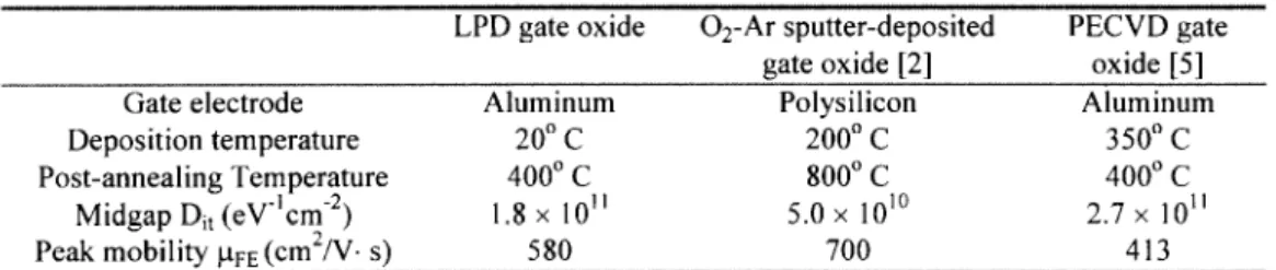
Since the MOSFET mobility is strongly influenced by the surface states, it is essential to evaluate the mobility when investigating the interface quality. Fig. I1 shows the field-effect mobility (pra) vs. the Vo- Vr. The prE is given by uLFE = g,,,, L/Z. C,,. Vo, where C,, is the gate capacitance per unit area. The mobility curves are highly consistent with those of MOSFETs with thermal gate oxide [9]. The peak pm is 580 cm’/V. s. The fact that mobility decreasing with gate voltage can be attributed to the enhanced surface roughness scattering with increased gate voltage [9]. In comparison with other works, our peak prE is larger than 413 cm2iV. s [5] but is less than 700 cm’/V. s of another work [2]. These results show that the
C. F. Yeh et al. / Microelectronic Engineering 28 (1995) 101-104 103
interface properties of Si/LPD oxide are superior to those of Si/PECVD SiOz, but inferior to those of Si/02- Ar sputter-deposited oxide. We may confirm this result from the Dir data, as shown in Table I, where the parameters calculated from MOSFET with LPD oxide were summarized. The results of other MOSFETs with various low-temperature deposited gate oxides were also shown for comparison. It reveals that the Di, of our device is lower than that of sputtered oxide device, but higher than that of PECVD oxide device. The least Di, for the sputter-oxide device may be attributed to a high-temperature annealing, which was performed at 800°C after oxide deposition. The LPD oxide devices having less D’, may be due to fluorine incorporated in the film [IO], as shown in the above section. That is, the fluorine may passivate some interfacial dangling bonds, as well as remove some Si-Si and Si-0 weak bonds, via its incorporation and Si-F formation. Thus, the MOSFET with LPD oxide has excellent interface properties.
IV. CONCLUSION
We have applied a novel room-temperature LPD oxide to low-temperature processed MOSFET without high-temperature annealing. Its Io-Vn and ID-Vo curves exhibit excellent triode-like characteristics and subthreshold characteristics, respectively. All the device parameters were compared well to those of other low-temperature processed MOSFETs. These results reveal the great possibility of applying LPD oxide as a gate insulator in low-temperature processed MOSFET in future.
ACKNOWLEDGMENT
This work was supported by National Science Council, Republic of China, under contract number NSC-83-0404-E-009-121.
REFERENCES
[I] D. A. Baglee, J. Vuc. Sci. Technol. A, 4 (1986) 1002.
[2] S. Suyama, A. Okamoto, and T. Serikawa, ZEEE Trans. Electron Devices., ED-34 (1987) 2124. [3] J. Stasiak, J. Batey, and E. Tierney, IEEE Trans. Electron Devices., ED-34 (1987) 2367. [4] J. Lee, I.-C. Chen, and C. Hu, IEEE Electron Device Lett., EDL-9 (1988) 324.
[5] J. Stasiak, J. Batey, E. Tierney, and J. Li, IEEE Electron Device Lett., EDL-10 (1989) 245.
[6] C. F. Yeh, S. S. Lin, C. L. Chern, and Y. C. Yang, IEEE Electron Device Letters, EDL-14 (1993) 403. [7] C. F. Yeh, S. S. Lin, T. Z. Yang, C. L. Chern, and Y. C. Yang, IEEE Trans. Electron Devices, ED-41 (1994) 173.
[S] C. F. Yeh and C. L. Chen, Journd of Electrochem. Sot., 141 (1994) 3 177. [9] S. C. Sun and J. D. Plummer, IEEE Trans. Electron Devices, ED-27 (1980) 1497. [IO] D. N. Kouvatsos et al, J. Electrochem. Sot., 140 (1993) 1160.
TABLE I. SUMMARIES OF DEVICE PERFORMANCES FOR MOSFETs UTILIZING
VARIOUS GATE OXIDE DEPOSITION METHODS
LPD gate oxide 02-Ar sputter-deposited PECVD gate gate oxide [2] oxide [5]
Gate electrode Aluminum Polysilicon Aluminum
Deposition temperature 2o” c 2oo” c 350° c
Post-annealing Temperature 4oo” c 800° c 4oo” c
Midgap Di, (eV“cmm2) 1.8 x IO” 5.0 x 1o’O 2.7 x 10”
104 C. F. Yeh et al. / Microelectronic Engineering 28 (1995) 101-104
n+ I I n+ I I n+
Atomic Force Microscope (AFM)
Figure 3. AFM surface
inspection of LPD oxide deposited with the circu-lation apparatus.
Sodn tank P-substrate
Figure 1. Schematic d ia gram of Figure 2. The cross-sectional
the circulation apparatus for LPD oxide.
view of the fabricated MOSFET device. Temperature j”C) 20 0 l--J 012345676 Q
L--
0 25 50 75 1W 125 150 175 04,400 13bO 1200 IlbO @IQ 9bQ 8bQ
Wavenumher (cm-l)
Figure 7. FTIR spectra of
LPD oxide and thermal oxide in the region of 700 - 1400 cm-l
Breakdown Field (MVicm) Hz0 Added Quanl~jml)
Figure 6. Relationship
between deposition rate of LPD oxide and deposition temperature.
Figure 4. Breakdown Figure 5. Relationship
field distribution of LPD bet-ween deposition rate oxide deposited with the of LPD oxide and Hz0 circula-tl’on apparatus. added quantity.
1 VG’IV 0 2 4 6 6 0 2 4 6 6 vG_vT iv) Figure 11. pm versus VG-VT of MOSFETs with LPD oxide as gate insulator.
24661. II
El&c held &fVicm)Q Drain Voltage VD (v)
Figure 8. J vs. E charac- Figure 9. The typical ID-
teristics of MOS diode
with LPD oxide as gate VD characteristics of
insulator. MOSFETs with LPD
oxide as gate insulator.
Gale Voltage (v)
Figure 10. The typical
ID-VG characteristics of MOSPETs with LPD oxide as gate insulator.