Abstract— A reliable temporary bonding scheme with both inorganic amorphous silicon release layer and HD-3007 polyimide based on high 355-nm-wavelength laser absorption coefficient in release layer is proposed and investigated. Effects of laser absorption coefficient and laser ablation path are also studied to develop a high throughput laser ablation process. The bonding scheme can be achieved within the optimized temperature of 210°C under 1 MPa bonding force. In addition, chemical resistance, mechanical strength with reliability assessment, and thermal stability test for bonded structure are inspected. There is no obvious degradation in electrical characterization after laser ablation, indicating that the temporary bonding scheme has high potential to be used for 3D integration applications.
Index Terms—three-dimensional integration, temporary bonding, laser release
I. INTRODUCTION
HE desire to pursue smaller, thinner, and multifunctional
integration scheme is the motivation for the consumer
electronics in the market such as smartphone, tablets, wearable
device, and internet of things (IoT) [1]. Therefore,
three-dimensional integration and advanced packaging scheme
have been proposed as promising solutions for the
aforementioned pursue due to their advantages of small form
factor, low power consumption, and heterogeneous integration
in next generation semiconductor fabrication era [2-3]. The
platforms that utilized this technology include fan-out
wafer-level package (FOWLP), 2.5D interposers with through
silicon via (TSV), and 3D-IC high-density integration with TSV
interconnects [4]. The above-mentioned platforms involve a key
technology of mechanically supported thin wafer handling
through temporary bonding process [5].
The temporary bonded structure must meet the requirements
of chemical resistance ability for subsequent back-end-of-line
This work was supported in part by the Ministry of Science and Technology under Grant MOST 103-2221-E-009-173-MY3, Grant MOST 103-2221-E-009-193-MY3, and Grant MOST 102-2112-M- 001-020-MY3, and in part by the Ministry of Education in Taiwan under the ATU Program.
Chuan-An Cheng, Yu-Hsiang Huang, and Kuan-Neng Chen are with Department of Electronics Engineering, National Chiao Tung University, Hsinchu 300, Taiwan. (E-mail: [email protected]).
Chien-Hung Lin, Chia-Lin Lee and Shan-Chun Yang are with Kingyoup Optronics Co., Ltd, Taoyuan, Taiwan.
(BEOL) process, thermal stability during post fabrication
process with a temperature of 300°C or even higher, and reliable
mechanically bonding strength between a carrier wafer and an
ultra-thinned device wafer with thickness below 100 μm [6-7].
Moreover, release process temperature and high throughput are
both significant factors that have to be taken into consideration
in the de-bonding technology. The prior arts have shown several
useful temporary bonding scheme and release methods to
achieve the demand of manufacturing process [6-8].
In this paper, a new bonding structure constituted with both
high UV absorption inorganic amorphous silicon as release
layer and the HD-3007 polyimide as adhesive layer is
demonstrated. The bonding structure is used for temporary
bonding platform that utilizes carrier glass wafer and
amorphous indium gallium zinc oxide (a-IGZO) thin-film
transistors (TFTs) device wafer with room temperature high
throughput laser ablation procedure. Although amorphous
silicon as release layer has been successfully implemented with
the adhesive layer of spin on glass (SOG) in Tohoku University
[9], the distinct structure with more detailed inspection for laser
release technology is carried out in this paper. Hence, using the
proposed promising bonding structure with high throughput
laser release scheme can be an attractive option for 3D
integration and advanced packaging applications.
II.
T
EMPORARY BONDING AND LASER RELEASE PROCEDUREFig. 1 shows the schematic process flow of temporary
bonding with fabricated device integration scheme. The key
technologies used are temporary bonding and laser release
process. Amorphous IGZO TFT is fabricated through the
process of photolithography, IGZO/TaN active/contact layer
sputtering, and oxide layer deposition. HD-3007 polyimide
adhesive layer is spin-coated and fully imidized at 300
oC for 30
min on the device wafer before bonding. The photolysis
polymer has been utilized as a release layer with great bonding
result as well as good laser ablation quality [10-11]. In addition,
the promising candidate material of 250-nm-thick amorphous
silicon with higher absorption coefficient than photolysis
polymer is deposited by HDP-CVD on the carrier glass wafer
(Corning Inc. Eagle XG glass wafer) with the presence of
boro-aluminosilicate. The device wafer is bonded face-to-face
with the carrier glass wafer for 10 min under 1 MPa bonding
Feasibility Investigation of Amorphous Silicon
as Release Layer in Temporary Bonding for 3D
Integration and FOWLP Scheme
Chuan-An Cheng,
Yu-Hsiang Huang, Chien-Hung Lin, Chia-Lin Lee, Shan-Chun Yang
and Kuan-Neng
Chen, Senior Member, IEEE
force in the 1.33x10
-7hPa vacuum chamber. Subsequently, laser
release process is applied for the bonded structure between the
polyimide adhesive layer and amorphous silicon release layer at
room temperature. Finally, separation of the carrier wafer and
device wafer can be obtained without any extra force in a high
throughput scheme. In addition, the residue amorphous silicon
on both device wafer and glass wafer can be cleaned by
C
4F
8/SF
6chemistry dry-etching process with inductively
coupled plasma (ICP) [12]. Then the HD-3007 can be removed
with 60°C EKC-865 solvent in 5 min with a 40 kHz ultrasonic
treatment.
The wafer-level temporary bonding with amorphous silicon
and HD-3007 polyimide as release layer and adhesive layer is
successfully developed under 220°C low bonding temperature
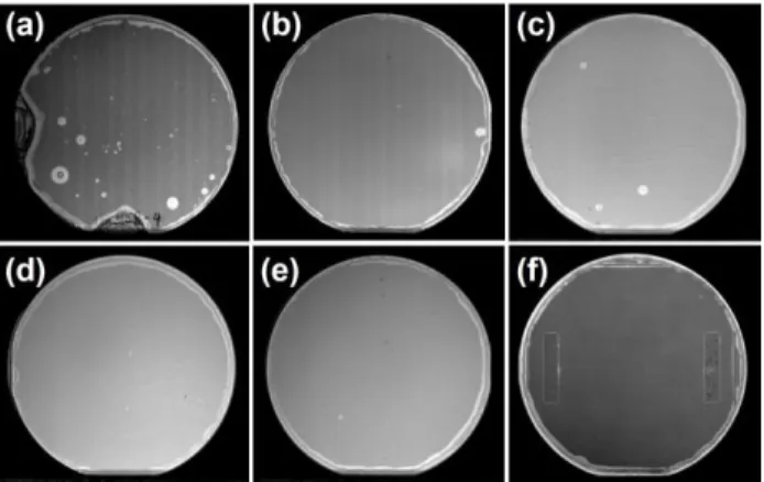
and 1 MPa bonding force. Figures 2(a)-(e) show the Scanning
Acoustic Tomography (SAT) images from 180°C to 220°C for
the inspection of the bonding quality [13]. Although some voids
can be seen when bonding temperature is below 210°C, an
entire well-bonded blanket wafer can be achieved when bonding
temperature is at 210°C. In addition, the amorphous IGZO TFT
device with optimized bonding temperature of 210°C in Fig. 2(f)
shows the void-free bonding quality, which demonstrates a
promising alternative for temporary bonding procedure.
The laser ablation mechanism is mainly focused on the
dry-etching process. The photon-energy from laser pulse shot is
projected onto the high absorption coefficient release layer, then
the molecular bonds are broken through the transition of the
material from solid phase to gas phase and some are ejected as
powder plume in the process [14]. To investigate the optical
characteristics of amorphous silicon, photolysis polymer, and
polyimide adhesive layer, these three materials are coated on
one glass wafer respectively, and then scanned from 300 nm to
1100 nm wavelength through a spectrometer to obtain their
transmittances. The absorption coefficient of three materials can
then be calculated.
Fig. 3 shows that the obvious difference of the absorption
coefficient among the adhesive layer, amorphous silicon, and
photolysis release layer at 355 nm wavelength. This indicates
that the UV wavelength can be absorbed into the amorphous
silicon and the photolysis release layer but not the adhesion
layer. In addition, the amorphous silicon has a higher absorption
coefficient than the photolysis polymer. Hence, unlike the
photolysis polymer used in prior art [10-11], 250-nm-thick
amorphous silicon, which does not require aging process before
bonding, is recommended as a great release layer for temporary
bonding.
The laser power density is about 196 mJ/cm
2when the laser
emission power is 2.5 W. To realize the throughput ability of
laser release process between amorphous silicon and photolysis
polymer, the ablated size with corresponding laser emission
power is investigated. The laser-ablated radius in the
amorphous silicon is slightly larger than in the photolysis
polymer, as shown in Fig. 4(a). Fig. 4(b) shows the well laser
release direction in meander shape with every pulse laser shot
overlapped by using a low-cost 355-nm diode-pumped
solid-state (DPSS) laser from KYO Laser De-bonder. The
throughput of laser ablation can be calculated using formula
(1)-(2):
2
R
f
pitch
Line
f
speed
Scan
……. (1)
f
R
A
speed
Scan
pith
Line
A
time
Release
22
……. (2)
Where R is the laser-ablated radius of the release area, A is
the laser-released area, and f is the frequency of laser
Fig. 1 Process flow of temporary bonding before and after laserablation process.
Fig. 3 The absorption coefficient of adhesive, amorphous silicon, and photolysis release layer under different wavelengths.
Fig. 2 SAT images of wafer-level bonding with different conditions as: (a) 180°C; (b) 190°C; (c) 200°C; (d) 210°C; (e) 220°C; and device wafer with (f) 210°C, 1 MPa.
auto-mechanical scanning system. Scanning line pitch is
designed as the distance between two centers of the ablation
area. In addition, the laser release time for a 100-mm wafer in
diameter in this study is less than 15 s when amorphous silicon
is used as release layer. Therefore, larger ablated size in the
amorphous silicon release layer lead to shorter laser release time
and higher throughput, which is suitable for 3D integration and
advanced packaging.
III. R
ELIABILITY ASSESSMENT OF BONDING SCHEMEIn order to validate the bonding strength and the impact of the
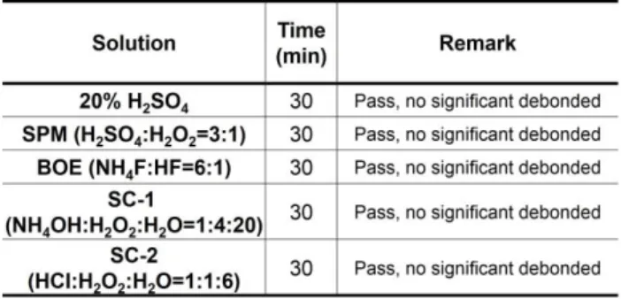
subsequent manufacturing processes on both release layer and
adhesive layer, a chemical resistance assessment is examined
with five types of acid and alkaline solutions. Table I shows the
results of the bonded structure of amorphous silicon and
HD-3007 polyimide [13]. The bonded structure remains the
same without de-lamination even after being assessed for 30
minutes, indicating the feasibility of a reliable bonded structure
between device wafer and carrier wafer.
For the purpose of assessing the bonding strength of the
bonded structure between amorphous silicon and HD-3007
polyimide, pull test is carried out to evaluate mechanical
characteristics on the diced bonded chip with size of 2 cm x 2
cm. The optimized bonding temperature at 210°C has the
highest bonding strength of 5.07 MPa with estimated error of
15% as shown in Table II, which has the similar result as SAT
images in Fig. 2(d). Moreover, the environmental conditions of
BEOL fabrication procedure and reliability assessment are also
considered. Therefore, a humidity test with the conditions of a
40% humidity at 25°C in 75 days and un-bias standard highly
accelerated stress test (un-bias HAST) based on JESD22A-118
with the conditions of 85% humidity at 130°C are utilized to
realize the degree of decline in the mechanical strength of the
bonded structure. The results of the mentioned reliability
assessment conditions in Fig. 5 indicate that the optimized
bonding temperature at 210°C has the highest bonding strength
as compared to the others.
Fig. 6 Pull-test results at different assessment temperature within 10 min, 30 min, and 60 min.
TABLE I
RESULTS OF BONDED STRUCTURE FOR CHEMICAL RESISTANCE ASSESSMENT
Fig. 4 (a) OM images of laser ablated on photolysis polymer and amorphous silicon at different laser power. (b) Laser release direction with overlapped ablation area in meander shape.
TABLE II
PULL-TEST RESULTS AT DIFFERENT BONDING TEMPERATURE AND RELIABILITY ASSESSMENT
Fig. 5 Pull-test results at different bonding temperature from 180°C to 220°C and environmental reliability assessment.
Thermal stability test is another emphasis for the post
integration process, which includes PECVD and permanent
bonding after temporary bonding procedure. Therefore, the pull
test investigation for the post annealing process with nitrogen
flow in the oven from 150°C to 350°C within 10 min, 30 min,
and 60 min are assessed with estimated error of 15% on the
bonded structure respectively. Fig. 6 shows that when the
annealing temperature is at and below 300°C, the bonding
strength has only a slight variance without degradation with an
increased in annealing time. As a result, great thermal stability
for the temporary bonded structure can be realized at
temperature below 300°C.
IV. A-IGZO
TFT
ELECTRICAL BEHAVIOR BEFORE AND AFTER LASER ABLATIONTo consider the applicable laser release process for real
device applications, two types of amorphous IGZO thin-film
transistor device have been assessed. Almost overlapping
results without deterioration of drain current before and after the
laser ablation process in TFT gate length of 30 μm and 70 μm
demonstrate reliable electrical characteristic as shown in Fig. 7.
The results prove the high reliability of this temporary bonding
platform using amorphous silicon and adhesive polymer bonded
structure during the laser ablation procedure.
V.
C
ONCLUSIONIn this study, a temporary bonding scheme with polyimide
adhesive layer and amorphous silicon inorganic release layer
has been successfully demonstrated. With a 250-nm-thick high
UV absorption coefficient release layer of amorphous silicon,
excellent bonding quality at bonding temperature of 210°C,
great chemical resistance, mechanical strength, thermal stability
below 300°C, and reliable electrical behavior before and after
laser release process are achieved. In addition, the low-cost
355-nm diode-pumped solid-state (DPSS) laser de-bonder and
auto-mechanically applicable ablation direction in meander
path lead to high throughput fabrication for laser ablation
procedure. The successful implementation and assessed results
indicate the feasibility of amorphous silicon as a promising
candidate for temporary bonding in 3D integration and
advanced packaging.
R
EFERENCES[1] Ramachandran K. Trichur, Tony D. Flaim, "Temporary bonding and thin wafer handling strategies for semiconductor device processing," Chip Scale Review, vol. 19, pp. 38-41, 2015.
[2] F. Liu, R. R. Yu, A. M. Young, J. P. Doyle, X. Wang, L. Shi, K.-N. Chen, X. Li, D. A Dipaola, D. Brown, C. T. Ryan, J. A Hagan, K. Wong, M. Lu, X. Gu, N. Klymko, E. Perfecto, A. G. Merryman, K. Kelly, S. Purushothaman, S. J. Koester, R. Wisneieff, and W. Haensch, “A 300-mm Wafer-Level Three-Dimensional Integration Scheme Using Tungsten Through-Silicon Via and Hybrid Cu-Adhesive Bonding,” 2008 International Electron Devices Meeting (IEDM), San Francisco CA, Dec. 15-17, 2008. DOI: 10.1109/IEDM.2008.4796762
[3] R. R. Yu, F. Liu, R. J. Polastre, K.-N. Chen, X. H. Liu, L. Shi, E. D. Perfecto, N. R. Klymko, M. S. Chace, T. M. Shaw, D. Dimilia, E. R. Kinser, A. M. Young, S. Purushothaman, S. J. Koester and W. Haensch, “Reliability of a 300-mm-compatible 3DI technology based on hybrid Cu-adhesive wafer bonding,” 2009 Symposia on VLSI Technology and Circuits, Kyoto, Japan, Jun. 15-18, 2009.
[4] Ramachandran K. Trichur, Tony D. Flaim, "Evolution of temporary bonding technology for advanced semiconductor packaging," Chip Scale Review, vol. 20, pp. 12-18, 2016.
[5] B. Dang, B. Webb, C. Tsang, P. Andry, and J. Knickerbocker, "Factors in the selection of temporary wafer handlers for 3D/2.5 D integration," Proc 64th Electronic Components and Technology Conference, Orlando, FL,
May 27-30,2014, pp. 576-581. DOI: 10.1109/ECTC.2014.6897343 [6] W. L. Tsai, H. H. Chang, C. H. Chien, J. H. Lau, H. C. Fu, C. W. Chiang,
T. Y. Kuo, Y. H. Chen, R. Lo, and M. J. Kao, "How to select adhesive materials for temporary bonding and de-bonding of 200mm and 300mm thin-wafer handling for 3D IC integration?," Proc 61th Electronic
Components and Technology Conference, Lake Buena Vista, FL, May 31-June 3, 2011, pp. 989-998. DOI: 10.1109/ECTC.2011.5898630 [7] K. Zoschke, T. Fischer, M. Topper, T. Fritzsch, O. Ehrmann, T. Itabashi,
Melvin P. Zussman, Matthew Souter, H. Oppermann, and K.-D. Lang,"Polyimide based temporary wafer bonding technology for high temperature compliant TSV backside processing and thin device handling," Proc 62th Electronic Components and Technology Conference,
San Diego, CA, May 29-June 1, 2012, pp. 1054-1061. DOI: 10.1109/ECTC.2012.6248966
[8] M. Zussman, C. Milasincic, A. Rardin, S. Kirk, and T. Itabashi, "Using permanent and temporary polyimide adhesives in 3D-TSV processing to avoid thin wafer handling," Journal of Microelectronics and Electronic Packaging, vol. 7, p. 214, 2010. DOI: 10.4071/imaps.260
[9] H. Hashiguchi, T. Fukushima, H. Kino, K-W. Lee, T. Tanaka1, M. Koyanagi, “A New Temporary Bonding Technology with Spin-on Glass and Hydrogenated Amorphous Si for 3D LSls,” International conference on electronics pakaging (ICEP), Toyama, April 23-25, pp. 74-77, 2014. DOI: 10.1109/ICEP.2014.6826664
[10] Tsung-Yen Tsai, Chien-Hung Lin, Chia-Lin Lee, Shan-Chun Yang, and Kuan-Neng Chen, “An ultra-fast temporary bonding and release process based on thin photolysis polymer in 3D integration,” 3D System Integration Conference (3DIC), Sendai, Aug 31-Sept 2, 2015. DOI: 10.1109/3DIC.2015.7334613
[11] Chuan-An Cheng, Yu-Hsiang Huang, Chien-Hung Lin, Chia-Lin Lee, Shan-Chun Yang, and Kuan-Neng Chen “Wafer-level MOSFET with submicron photolysis polymer temporary bonding technology using ultra-fast laser ablation for 3DIC application,” International Symposium on VLSI Technology, Systems and Application (VLSI-TSA), Hsinchu,
Taiwan, April 25-27, pp. 1-2, 2016. DOI:
10.1109/VLSI-TSA.2016.7480487
[12] Harvey-Collard, Patrick, Jaouad, Abdelatif, Drouin, Dominique, and Pioro-Ladrière, Michel, “Inductively Coupled Plasma etching of
amorphous silicon nanostructures over nanotopography using C4F8/SF6 chemistry,” Microelectronic Engineering, vol 110, pp. 408-413, 2013. [13] Yu-Hsiang Huang, Hao-Wen Liang, Chuan-An Cheng, Chien-Hung Lin,
Chia-Lin Lee, Shan-Chun Yang, and Kuan-Neng Chen, “Study of a Novel Amorphous Silicon Temporary Bonding and Corresponding Laser Assisted De-bonding Technology,” 2016 IEEE Electronic Components Fig. 7 Id-Vg behavior of a-IGZO TFT in gate length of 30 μm and
and Technology Conference (ECTC), Las Vegas, NV, USA, May 31 – Jun. 3, 2016. DOI: 10.1109/ECTC.2016.308
[14] Habib Hichri, Markus Arendt, Matthew Gingerella, “Novel Process of RDL formation for Advanced Packaging by Excimer Laser Ablation,” 2016 IEEE Electronic Components and Technology Conference (ECTC), Las Vegas, NV, USA, May 31 – Jun. 3, 2016. DOI: 10.1109/ECTC.2016.225
Chuan-An Cheng received the B.S. degree in physics from National Chung Hsing University (NCHU), Taichung, Taiwan, in 2009.
Currently, he is working toward Ph.D. degree at the Institute of Electronics Engineering, National Chiao Tung University (NCTU), Hsinchu, Taiwan. His research interests focus on 2.5D electronic packaging, fan-out wafer level package (FOWLP), wafer level bonding technology, through silicon via (TSV), heterogeneous integration, and three-dimensional integrated circuit technologies.
Yu-Hsiang Huang received the B.S. degree from the department of electrophysics, and the M.S. degree in department of photonics from National Chiao Tung University (NCTU), Hsinchu, Taiwan.
Currently, he is a product engineer in Etron technology, Inc., Hsinchu, Taiwan.
Chien-Hung Lin Chien-Hung Lin received his Ph.D. degree in Graduate Institute of Photonics and Optoelectronics from National Taiwan University (NTU), and his M.S. degree in Department of Physics from Chung Yuan Christian University (CYCU).
He was the research & development engineer in AU Optronics Co. to research on the amorphous and microcrystalline silicon thin film solar cells and heterojunction with intrinsic thin layer solar cell in 2010 ~ 2012. In 2013, he acted as deputy technical manager in Topcell-Solar International Co. of United Microelectronics Co. Group to research and develop advance technology in high efficiency solar cell. In 2013~2014, he worked as the project manager in General Interface Solution Co. of Foxconn Group to be responsible for leading team numbers to research and evaluate advance technologies, as force sensor and metal mesh imprinting, for using in high-end touch cell phone.
He is currently Director of Semiconductor Technology R&D Project Division in Kingyoup Optronics Co., Ltd. He dedicated to research on semiconductor package technology and to develop advanced process equipment on the semiconductor applications.
Chia-Lin Leereceived the M.S. degree in physics
from Tamkang University, New Taipei City, Taiwan, in 2009.
He is currently a section manager of research and development department in Kingyoup Optronics Co., Ltd. His research on advanced semiconductor package technology, colossal magnetoresistance material (CMR), and physical vapor deposition (PVD) technology.
Shan-Chun Yangreceived her B.S. degree in
Chemical Engineering and Materials Science from Tamkang University, New Taipei City, Taiwan.
Currently, She is an engineer of research and development department in Kingyoup Optronics Co., Ltd. She dedicated to research on semiconductor package technology and to develop advanced process equipment on the semiconductor applications.
Kuan-Neng Chen (M’05–SM’11) received his Ph.D. degree in Electrical Engineering and Computer Science, and his M.S. degree in Materials Science and Engineering, both from Massachusetts Institute of Technology (MIT). He is currently a professor of Department of Electronics Engineering in National Chiao Tung University. Prior to the faculty position, he was a Research Staff Member at the IBM Thomas J. Watson Research Center.
Dr. Chen has received four times of NCTU Distinguished Faculty Award, three times of NCTU Outstanding Industry-Academia Cooperation Achievement Award, CIEE Outstanding Professor Award, Adventech Young Professor Award, and EDMA Outstanding Service Award. He also holds five IBM Invention Plateau Invention Achievement Awards.
Dr. Chen has authored more than 250 publications and holds 77 patents. He has given more than 70 invited talks in industries, research institutes, and universities worldwide. He is currently the committee member of IEEE 3DIC, IEEE SSDM, IEEE VLSI-TSA, IMAPS 3D Packaging, and DPS. Dr. Chen is a member of Phi Tau Phi Scholastic Honor Society and senior member of the IEEE. Dr. Chen’s current research interests are three-dimensional integrated circuits (3D IC), through-silicon via (TSV) technology, wafer bonding technology, and heterogeneous integration.