822 IEEE MICROWAVE AND WIRELESS COMPONENTS LETTERS, VOL. 19, NO. 12, DECEMBER 2009
A K-Band CMOS Quadrature Frequency
Tripler Using Sub-Harmonic Mixer
Chien-Nan Kuo, Member, IEEE, Huan-Sheng Chen, and Tzu-Chao Yan
Abstract—A low-power frequency tripler is designed by using
the sub-harmonic mixer configuration for K-band applications. The proposed circuit features quadrature signal generation, applicable to LO signal synthesis in millimeter-wave wireless transceivers. It achieves conversion gain of 5.7 dB at the output frequency of 21 GHz. Implemented in a 0.18 m CMOS tech-nology, the circuit consumes power of 7.5 mW with 1.5 V supply voltage. The entire die occupies an area of1000 1050 m2.
Index Terms—Doubler, frequency mixing, frequency
multiplica-tion, tripler.
I. INTRODUCTION
F
REQUENCY multiplication is a popular method to gen-erate a high-frequency signal from the harmonic outputs of a low-frequency fundamental source. The frequency doubler is widely used, but a frequency tripler is better for high fre-quency signal generation. It can be found useful, for example, for LO signal generation in a 60 GHz wireless transceiver [1].Traditionally tripler design often relies on the nonlinear device characteristic of a diode or transistor in overdriven configurations [2]. Injection of the fundamental input signal produces the third-order harmonic output in the clipped output waveform. Typically it requires large power consumption to enhance the nonlinear effi-ciency. Proposed in [3] is a time-waveform shaping technique. It enhances the third-order harmonic by pulling the output voltage three times in each fundamental cycle. This approach becomes less efficient in millimeter-wave frequencies limited by transistor switching. Another technique is an indirect method by injection locking to a free-running oscillator around the third-order har-monic frequency [4]. It consumes less power since only a small harmonic output level is required from the nonlinear generator. But injection locking usually occurs in a very limited frequency range.
In this work, a CMOS quadrature frequency tripler is pro-posed using frequency mixing. Sub-harmonic mixers are ap-plied to produce the third-order harmonic output. The concept has been proved recently [5]. Additionally, the proposed circuit features quadrature signal generation with coupled I/Q signal paths. This novel architecture achieves maximum conversion
Manuscript received May 01, 2009; revised September 01, 2009. Current ver-sion published December 04, 2009. This work was supported by the National Science Council of Taiwan under Grant NSC 97-2220-E009-010, the MediaTek Center at NCTU, the ITRI JDR center at NCTU, by the Chip Implementation Center (CIC), and by Ansoft Corp.
The authors are with the Department of Electronic Engineering, National Chiao-Tung University (NCTU), Hsinchu 300, Taiwan (e-mail: cnkuo@mail. nctu.edu.tw).
Color versions of one or more of the figures in this letter are available online at http://ieeexplore.ieee.org.
Digital Object Identifier 10.1109/LMWC.2009.2033529
Fig. 1. Block diagram of the proposed frequency tripler.
gain (C.G.). The technique is verified by a K-band signal gener-ator in a 0.18 CMOS technology. Using single-balance de-sign, the circuit achieves frequency multiplication very power efficiently.
II. TRIPLERDESIGN
The block diagram of the proposed frequency tripler is as shown in Fig. 1. The tripler features quadrature signals at both the input and output. The fundamental quadrature I/Q input sig-nals at the frequency are first used to generate the second-order harmonics at by frequency doublers. Then the dou-bler outputs are mixed with the fundamentals to produce the quadrature third-order harmonic outputs at the frequency . Bandpass filters are placed at the mixer outputs to suppress un-desired spurs. As explained later, cross-coupling between I and Q paths not only keeps the quadrature characteristic but also al-lows maximum frequency conversion efficiency.
In circuit implementation, the frequency doubler and the mixer can be realized in a cascode configuration, known as the sub-harmonic mixer [6]. The schematic of the tripler core circuit as a single-balance mixer is shown in Fig. 2. This cur-rent-reuse topology is advantageous in low power consumption. Two differential input signals, and , of the same magni-tude are fed into two transistor pairs. The bottom transistor pair forms an efficient frequency doubler. It generates the output current at to drive the top source-coupled dif-ferential pair , which works as the switching stage of the mixer. This mixer produces the third-order harmonic by frequency up-conversion of current commutation.
Circuit operation relies on the second-order nonlinearity in both transistor pairs. To maximize the efficiency of frequency conversion, each transistor should be biased at the gate voltage for the maximum voltage derivative of device transconductance . Besides, the input signals to the two transistor pairs are at the same frequency in this circuit, different from the operation in a typical sub-harmonic mixer. The phase difference between and critically determines the frequency conversion gain. Fig. 3 shows the simulation result of the normalized third-order
KUO et al.: K-BAND CMOS QUADRATURE FREQUENCY TRIPLER 823
Fig. 2. Schematic of the tripler core circuit, including the doubler and the mixer.
Fig. 3. Contour plot of the normalized third-order harmonic output current by sweeping the two input signals at the frequency of 7 GHz.
output current by sweeping the two input signals at . The output current is insensitive to the magnitude imbalance. The mixer generates very small output current if the signals are in phase and maximum output current if the voltages are around 90 degrees out of phase. It was found that the optimal phase difference moves close to 90 degrees as the operation fre-quency decreases. Therefore, the tripler circuit requires a pair of quadrature I/Q input signals. Furthermore, the output current phases of the two core circuits in Fig. 1 are also in quadrature to each other. This property is very useful for LO generation.
The mixer load affects the tripler conversion gain [7]. It is ob-served that the load impedance should be low at the frequencies and , while high at . A bandpass filter provides the re-quired impedance condition and suppresses out-of-band spurs as well. It is implemented by a resonator utilizing an inductor and the parasitic capacitor at the output node.
III. MEASUREMENTRESULTS
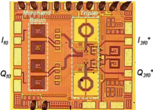
The tripler circuit is designed and fabricated in a 0.18 CMOS technology. The die micrograph is shown in Fig. 4, oc-cupying an area of , but the I/Q tripler circuit only takes . An off-chip 90 hybrid coupler is used to produce the two quadrature input signals, and . Two on-chip Marchand baluns at the input convert the signal into the differential format to drive the tripler, one for I path and the other for Q path. Open-drain buffers are used at the mixer output for the measurement purpose. Based on simulations, the balun and buffer introduce extra signal loss of 16.7 dB at 7 GHz.
Fig. 4. Micrograph of the fabricated frequency tripler.
Fig. 5. Snapshot of measured raw data showing the output spectra with the input signal at 7 GHz. (Note: cable loss is not calibrated yet.)
Fig. 6. (a) Power transfer at input/output frequency of 7/21 GHz, and (b) fre-quency response of conversion gain. (Note:P is the power level at the balun input.)
In a fully integrated environment, the signal loss could be elimi-nated with direct I/Q inputs. In this work, the input signal power only can be calibrated to the balun input during measure-ments. The conversion gain of the tripler is thus calculated by subtraction of the simulated loss.
Fig. 5 shows a snapshot of the measured output spectrum with an input signal of 10 dBm at 7 GHz. The power level at the chip output is 12.4 dBm after calibration of cable loss. The cal-culated conversion gain achieves 5.7 dB, excluding the balun and buffer. The power transfer curve is plotted in Fig. 6(a). The output power increases as the input signal level increases, but eventually saturates at of 14 dBm. The curve slope is close to 2, corresponding to the sub-harmonic mixer operation. The
824 IEEE MICROWAVE AND WIRELESS COMPONENTS LETTERS, VOL. 19, NO. 12, DECEMBER 2009
Fig. 7. Measured harmonic rejection ratios (HRR) withP = 10 dBm.
Fig. 8. Measured phase noise of input and output signals.
frequency response of the conversion gain with
is plotted in Fig. 6(b). The maximum conversion gain occurs at the output frequency of 21 GHz.
Ideally the output signal only appears at . Frequency mixing inevitably introduces undesired spurs. To identify signal purity, a parameter of the harmonic rejection ratio (HRR) is defined as
(1) where n refers to the nth-order harmonic. Fig. 7 show the mea-sured HRR of several harmonic outputs. The HRRs of the first-order, second-first-order, and fourth-order with the input signal of 7 GHz are 22.44 dBc, 16.1 dBc and 20.18 dBc, respectively. Since the circuit is fully differential, the second-order leakage is not critical in practical applications.
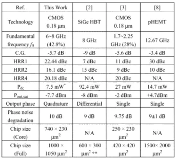
The measured phase noise of the input and output signal is shown in Fig. 8. The phase noise measured at 1 MHz offset of the 7 GHz input signal source and the third-order output are 140.5 dBc/Hz and 130.5 dBc/Hz, respectively. This differ-ence, around 10 dB, is consistent over the offset frequency range below 1 MHz. This difference agrees well with the theoretical value of 9.5 dB corresponding to the multiplication ratio of 3. The increased noise floor above 1 MHz is likely due to the noise of this tripler. With , the tripler in operation con-sumes a power of 7.5 mW with . Table I summa-rizes the performance comparison between the proposed tripler and published results in literature [8].
TABLE I
PERFORMANCESUMMARY ANDCOMPARISON
Power consumption includes I/Q paths (core) with the input power of 10 dBm at the balun input. Power consumption of buffers is 32.13 mW.
Including VCO and tripler.
IV. CONCLUSION
A novel CMOS quadrature frequency tripler using sub-har-monic mixers is proposed to efficiently generate the third-order harmonic of the input frequency. The proposed tripler produces quadrature output signals, while drawing the lowest power level of 7.5 mW with 1.5 V supply, as compared to other works. It can be applied to signal generation in the millimeter-wave applications.
REFERENCES
[1] B. A. Floyd, “A 16–18.8-GHz sub-integer-N frequency synthesizer for 60-GHz transceivers,” IEEE J. Solid-State Circuits, vol. 43, no. 5, pp. 1076–1086, May 2008.
[2] M. Danesh, F. Gruson, P. Abele, and H. Schumacher, “Differential VCO and frequency tripler using SiGe HBTs for the 24 GHz ISM band,” in IEEE RF Integrated Circuits Symp., Philadelphia, PA, Jun. 2003, pp. 277–280.
[3] Y. Zheng and C. E. Saavedra, “A broadband CMOS frequency tripler using a third-harmonic enhanced technique,” IEEE J. Solid-State
Cir-cuits, vol. 42, no. 10, pp. 2197–2303, Oct. 2007.
[4] M.-C. Chen and C.-Y. Wu, “Design and analysis of CMOS sub-harmonic injection-locked frequency triplers,” IEEE Trans. Microw.
Theory Tech., vol. 56, no. 8, pp. 1869–1878, Aug. 2008.
[5] B. R. Jackson, F. Mazzilli, and C. E. Saavedra, “A frequency tripler using a subharmonic mixer and fundamental cancellation,” IEEE
Trans. Microw. Theory Tech., vol. 57, no. 5, pp. 1083–1090, May
2009.
[6] Z. Zhang, Z. Chen, L. Tsui, and J. Lau, “A 930 MHz CMOS DC-offset free direct-conversion 4-FSK receiver,” in IEEE Int. Solid-State
Cir-cuits Conf., San Francisco, CA, Feb. 2001, pp. 290–291.
[7] J. E. Johnson, G. R. Branner, and J.-P. Mima, “Design and optimization of large conversion gain active microwave frequency triplers,” IEEE
Microw. Wireless Compon. Lett., vol. 15, no. 7, pp. 457–459, Jul. 2005.
[8] A. Boudiaf, D. Bachelet, and C. Rumelhard, “A high-efficiency and low-phase-noise 38-GHz pHEMT MMIC tripler,” IEEE Trans.