K and Au Bicatalyst Assisted Growth of Carbon Nanocoils from
Acetylene: E
ffect of Deposition Parameters on Field Emission
Properties
Tsung-Yu Tsou,
†Chi-Young Lee,
‡and Hsin-Tien Chiu*
,††Department of Applied Chemistry, National Chiao Tung University, Hsinchu, Taiwan, 30050, R. O. C.
‡Department of Materials Science and Engineering, National Tsing Hua University, Hsinchu, Taiwan, 30043, R. O. C.
*
S Supporting InformationABSTRACT: We demonstrated the growth of carbon nano-coils (CNCs) via chemical vapor deposition (CVD) using Au and K metals as the catalysts to assist the thermal decomposition of C2H2. Typical CNCs (wire diameter: 50−
80 nm, coil diameter: 110−140 nm, pitch: 100−200 nm, tens of micrometers), identified as amorphous coiled carbon fibers by scanning electron microscopy (SEM) and transmission electron microscopy (TEM), were grown at proper combina-tions of reaction parameters. Au nanoparticles (NPs), identified by energy dispersion X-ray spectroscopy (EDX)
and electron diffraction (ED), were located at the tips of the CNCs. The observations suggested that a tip-growth mechanism involving the Au NPs as the nucleation sites was in operation. In the reaction, the liquid-phase K metal assisted the decomposition of C2H2by lowering the reaction temperature. We propose that acetylide and hydride intermediates were formed in the reaction. Further decomposition of the acetylide intermediates generated solid-phase carbon to grow the CNCs. Effects of varying the reaction conditions on the CNC growth were investigated. On the basis of the results, a Au and K bicatalyst enhanced tip-growth vapor−liquid−solid (VLS) mechanism was proposed to rationalize the CNC formation process. Electron field emission (EFE) characteristics of the CNCs were studied. The best EFE result showed a turn-onfield (Eto) of 3.78 V/μm and a field enhancement factor (β) of 1852. In addition, the current density (J) was as high as 43 mA/cm2at 6.87 V/μm. The data
suggest that the CNCs could be employed forfield emission device applications. KEYWORDS: carbon nanocoils, Au catalyst, K catalyst,field emission
■
INTRODUCTIONVarious carbon nanomaterials, including carbon nanotubes (CNTs), carbon nanofibers (CNFs), carbon nanocoils (CNCs), and fullerenes, have been intensively investigated because of their intrinsic properties such as chemical stability, high mechanical strength, high external surface area, and good thermal and electrical conductivity.1−5They are used in a wide range of applications, including semiconductor devices, field emission devices, biomedical components, catalysis, electro-chemical electrodes, and analysis.6−19Among these nanostruc-tures, CNCs are expected to have special properties and possible unique applications because of their three-dimensional (3-D) helical morphologies. Several synthetic methods have been reported to fabricate CNCs. These include chemical vapor deposition (CVD), arc-discharge, flame synthesis, and hydro-thermal synthesis.13,20−22 Among them, CVD is the most widely used one. Many groups have employed CVD to grow CNCs via catalytic decomposition of hydrocarbons, employing many different metal catalysts.23−28Even though several growth mechanisms have been proposed to rationalize CNC growths, new pathways are still possible.29−32 Recently, we observed growth of CNCs by thermal decomposition of C2H2 on Si
substrates through a novel Ag and K bicatalyst assisted vapor− liquid−solid (VLS) tip-growth route.13 We suggest that K assisted the decomposition of C2H2by forming relatively stable
acetylide and hydride intermediates, while Ag nanoparticles (NPs) acted as the tips for the CNC growths. In addition, we propose that the affinities between the liquid-phase K and the as-deposited solid C caused the growing one-dimensional material to curl into coils. To explore other possible cases operated via this route and to seek better control of the CNCs’ uniformity, we report here the use of Au NPs and K as the bicatalysts to assist the thermal decomposition of C2H2 on
flexible graphite foils. The graphite substrates offer higher conductivity, lower cost than Si, and more potential to integrate CNCs into bendable electronic devices.
With proper control of the reaction parameters, uniformly shaped CNCs on the graphite substrates can be employed for electronfield emission (EFE) applications. EFE is a quantum tunneling process which extracts the electron from the material Received: August 2, 2012
Accepted: November 19, 2012 Published: November 20, 2012
surface into the vacuum level by applying a sufficient external electric field.33 The performance is sensitive to the composition, morphology, and aspect ratio of the emitting material. Among many potential materials, C-based emitters are widely explored due to their excellent physical and chemical properties.2−5,34−41 Because of their unique morphology, CNCs have shown excellent EFE characteristics.42,43 In this article, we wish to report our investigations on the factors affecting the growth of CNCs and the variables influencing their EFE properties.
■
EXPERIMENTAL SECTIONMaterials. Graphite foils (Alfa Aesar 99.8%, thickness: 0.5 mm) were used as the substrates. A Au target (99.99%) in a direct current (DC) sputtering system provided the source for the deposition of Au NPs on the substrates. KH powders (Sigma Aldrich, 30 wt % dispersion in mineral oil) were washed with anhydrous hexane and dried under an inert atmosphere prior to use. Locally supplied gases, C2H2(99.5%), H2(99.9999%), and Ar (99.9999%), were used in the reactions without further purification.
Growth of CNCs. The growth of a representative CNC sample, sample 22 listed in Table S1 in the Supporting Information, is described below. The graphite foil wasfirst cleaned with alcohol and acetone. A thin layer of Au was deposited on the substrate by DC sputtering (2.2 kV, 30−35 mA, background pressure 7 × 10⁻²mbar) for 20 s. Then, it was placed in a quartz boat (length: 10 cm) and loaded into a quartz tube inside a tube furnace (Lindberg Blue M, heated length: 61 cm). The boat was placed at 25 cm downstream from the center of the furnace. The system was evacuated andfilled with Ar several times to ensure an air-free reaction environment. Another quartz boat (length: 10 cm) loaded with KH powders (0.18 g) was placed at the center of the furnace under continuous Ar purge. Then, KH was thermally decomposed at 623 K (ramping rate 10 K min−1) in Ar for 1 h and cooled to 423 K gradually. After the reactor was evacuated below 10−3mbar, K was evaporated at 423 K to deposit a thin layer of K film on the substrate for 20 min. During the K deposition, the temperature at the substrate was 353−373 K. Then, under continuous Ar purge, the quartz boat loaded with the K- and Au-coated graphite substrate in the quartz tube was pulled to the center of the furnace. Then, at 723 K, C2H2(g) (2.7 sccm) and H2(g) (20 sccm) were passed over the substrate for 1 h. Growth of a black thinfilm on the substrate was observed. After the substrate was cooled to room temperature under Ar, K-containing byproducts were removed by deionized (DI) water. Finally, the product was dried in air before further characterizations. The growth parameters of other samples were listed in Table S1 in the Supporting Information also.
Instruments. Morphologies and compositions of the samples were characterized using field emission scanning electron microscopes (FESEM, Hitachi S-4000, Hitachi S-4700, and JEOL 7401F, at an accelerating voltage of 15 KeV) equipped with energy dispersive X-ray (EDX) systems. The crystallinity and microstructural details were studied using JEOL JSM-2010 (200 kV) and JEOL JEM-3000F (300 kV) high-resolution transmission electron microscopes (HRTEM).
Electrical Field Emission Measurements. EFE measurements were investigated using a homemade instrument. The high vacuum (2.5× 10⁻⁶mbar) testing system was equipped with an oil-free turbo-molecular pump (Alcatel ATP400C) and a rod-shaped tungsten anode (tip diameter: 2 mm) attached to an X−Y−Z manipulator. The EFE properties were determined using a simple diode configuration with the substratefixed on the sample stage as the cathode. The distance between the tip and the sample was adjusted by a micrometer on the manipulator. The emission currents were measured with a Keithley 2410 which also acted as the power supply (0−1100 V, with an increment of 20 V).
■
RESULTS AND DISCUSSIONSEM Characterizations. CNCs were grown on graphite substrates via CVD using Au and K metals as the catalysts. As
discussed below, the metals act cooperatively to assist the thermal decomposition of C2H2 and the coil growths. A
summary of the samples grown at various combinations of reaction conditions is shown in Table S1 in the Supporting Information. Analyses of a representative sample, 22, are described below as an example. In Figure 1, SEM images and an
EDX spectrum of 22 are shown. Figure 1A displays the presence of a high density of CNCs on the graphite substrate. In Figure 1B, a NP located at the tip of a CNC can be observed. An EDX analysis from the squared region in Figure 1B shows the signals of C, Au, K, and O. The K and O atoms can be removed by washing in DI water and are assigned to oxidized forms of K located mainly on the CNCs. The wire diameter, coil diameter, and pitch of the CNCs are determined to be 46− 88, 77−109, and 59−127 nm, respectively. Since the CNCs are entangled, their lengths are difficult to measure. From the thickness of the CNC layer on the substrate, we estimate that the coil lengths can be more than 10μm.
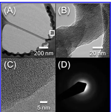
TEM Studies. To further characterize 22, TEM inves-tigations were carried out. The results are shown in Figures 2 and 3. Figure 2A shows the image of a CNC, with a coil diameter of 100 nm and a pitch of 100 nm. A high-magnification image in Figure 2B, from the squared region in Figure 2A, illustrates that the coil has a wire structure with a diameter of 40−50 nm. An HRTEM image in Figure 2C and a selected area electron diffraction (SAED) pattern in Figure 2D, also from the squared region, reveal that the coil body is amorphous. Figure 3 shows the data from another CNC. As shown in Figure 3A, the coil diameter is estimated to be 100 nm. In addition, a particle can be seen at the tip. An EDX spectrum of the particle, shown in Figure 3B, suggests that the particle contains Au mainly, and no signals from K are found. This agrees with the assumption that the oxidized forms of K were fully removed during the TEM sample preparation. The Cu signal is attributed to the Cu grid which held the sample. Figure 3C is the HRTEM image of the particle. From the image, a fringe spaced at 0.23 nm could be assigned to the lattice spacing of (111) planes of face-centered cubic (fcc) Au (JCPDS 89-3697). The SAED pattern in Figure 3D shows a single crystalline pattern from (11−1), (111), and (002) planes of fcc Au observed from the [−110] zone axis. Two sets of diffused ring patterns are also observed. They are assigned to the less ordered CNC structure.
Effect of Reaction Conditions on CNC Growths. A series of experiments with varied reaction conditions, as summarized in Table S1 in the Supporting Information, were
Figure 1.SEM images of as-grown CNCs in sample 22. (A) Low- and (B) high-magnification top-view images. Inset: EDX from squared region.
performed. The results suggest that the growth conditions affected the final products greatly. How these variables affected the morphology and property of the CNCs will be discussed below.
Figure S1 (Supporting Information) shows the effects of sizes of Au NPs (deposited by varying the sputtering time) and coating time of K metal on the C growths performed at 723 K. In Figure S1 (Supporting Information), A1−D1 display the SEM images of graphite substrates decorated with Au NPs
before the C depositions. Without the presence of K, no C nanostructures can be grown on these substrates (samples 5−8, images A2−D2 in Figure S1 (Supporting Information), correspondingly). On the other hand, in the reactions with just K on the substrates, only featureless C layers were obtained (images not shown). In contrast, in experiments with both Au and K deposited on the substrates, we observe the growths of C nanostructures in the forms of NPs, nanowires (NWs), and NCs (samples 1−4 and 9−12, images A3−D3 and A4−D4 in Figure S1 (Supporting Information), respectively). It has been known that both Na and K can function as dehydrogenation catalysts to assist the deposition of C from C2H2.
13,44
The images confirm the role of Au NPs as the nucleation seeds for the one-dimensional (1D) nanostructure formation again. Figure S2 in the Supporting Information shows size distribution histograms of the sputtered Au NPs on the substrates prior to the growths of 1−4. As the sputtering time is increased from 15 to 50 s, the average size of Au NPs increases from 30± 9 to 63 ± 21 nm. After the deposition of K on these substrates, NCs and curled NWs were obtained, as shown in Figure S3 in the Supporting Information for samples 1−4. Clearly, as the Au NP diameter increases, the NC and the NW diameters are increased as well. In general, CNCs were grown from smaller Au NPs (averaged size 30−39 nm), while curved NWs were the result of large Au NPs (average size 63 nm). Side-viewed C layer images (Figure S3C, F, I, and L, Supporting Information) also indicate that the density of the 1D products increases with the increasing density of Au NPs. Figure 4 summarizes the effect of the Au NP sizes on the CNC dimensions (wire diameter, coil diameter, and pitch). All of the results suggest that they are proportional to the Au NP sizes. The role of the Au NPs is supported further by the SEM images displayed in Figure 5. They reveal the nanostructures grown for only 2 min. For each individual nanostructure, a NP wrapped inside a curved 1D carbonfiber can be seen. On the basis of the data, the CNCs probably are grown via a NP assisted tip-growth mechanism.
To determine a proper carrier gas composition for CNC formation, the following conditions were attempted for experiments carried out at 723 K: H2 20 sccm, H230 sccm,
and Ar 20 sccm. SEM images of samples 2, 13, and 14 are displayed in Figure S4 (Supporting Information), respectively. Clearly, when H220 sccm was used, CNCs were formed in 2 (Figure S4A−C, Supporting Information). As shown in Figure S4D−F (Supporting Information), in the experiment using a high H2 flow rate of 30 sccm, not only the nanostructure
density decreases but also the morphology changes to worm-like NWs in 13. The above observations suggest that in an H2 -rich atmosphere more K surface sites are occupied by H atoms. This not only decreases the catalytic activity of K metal but also decreases the adhesion between the deposited C and the liquid surface of K. When Ar was used, only micrometer-sized C particles were obtained for 14 (Figure S4G−I, Supporting Information). We propose that in this H2-poor environment H
atoms on the K surface associate into H2 and desorb easily. This generates a H-poor K surface which can be covered by C atoms fully to form featureless C particles displayed in Figure S4G−I (Supporting Information).
To find proper CNC deposition rates, the reaction temperatures 673−773 K were attempted. Figure S5 (Support-ing Information) displays the morphologies of the C materials deposited in the experiments. Clearly, CNCs could not grow at 673 K in sample 15 (Figure S5A, Supporting Information),
Figure 2.TEM studies of a CNC in sample 22. (A) Low-magnification image. (B) High-magnification, (C) high-resolution, and (D) SAED pattern from the squared region in (A).
Figure 3.TEM studies of a CNC in sample 22. (A) Low-magnification image showing a NP at the tip. (B) EDX from the tip. (C) High-resolution image and (D) SAED pattern of the NP. The Cu signals in (B) are assigned to the TEM grid.
while at 773 K, sample 16, a Cfilm, was obtained (Figure S5B, Supporting Information). Obviously, at low temperatures, the overall growth rate was too low to offer CNCs. On the other hand, at high temperatures, the decomposition of C2H2was too fast to grow 1D products. Instead, a C film was deposited rapidly. The observations suggest that the reaction temperature influences the growth rate and the final morphology significantly. Only at 723 K, as shown in Figure S5C and D (Supporting Information), CNCs are found in sample 2. Thus, the temperature was selected as the optimized growth temperature for CNCs throughout this study.
After the proper carrier gas flow rate and the reaction temperature were selected, the effect of C2H2 flow rate on
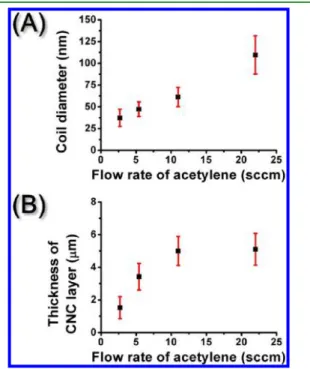
CNC morphology was examined. Figure S6 (Supporting Information) shows the CNCs (samples 2 and 17−19) grown at C2H2 flow rates of 2.7−22 sccm and 723 K for 20 min. The results are summarized in Table S2 in the Supporting Information. Using the data, the effect of the flow rate on the CNC diameter and layer thickness are plotted in Figure 6. As
theflow rate of C2H2is increased from 2.7 to 22 sccm, the coil
diameter increases from 37 nm for 2 to 110 nm for 19. The coil pitch does not change much. In addition, as theflow rate is increased from 2.7 to 11 sccm, the CNC layer thickens from 1.5 μm for 2 to 5.0 μm for 18. Although the layer thickness of 19 does not increase much at 22 sccm, its coil diameter widens significantly at this condition. In general, the amount of deposited C increases proportionally to the increased C2H2 flow rate. The results indicate that a high flow rate of C2H2
leads to a high concentration of the reactant near the reaction sites. Consequently, on the catalyst surface, the growth rate is enhanced, resulting in the increased coil diameter and the CNC layer thickness.
Figure S7 in the Supporting Information shows the SEM images of the CNCs 18, 20, and 21 grown at a C2H2flow rate
of 11 sccm and 723 K for 20−180 min. Using the morphological data displayed in the images, the averaged CNC diameters and layer thicknesses are summarized in Table S3 (Supporting Information) and plotted in Figure 7. It is reasonable to find that the CNC layer thickness increases proportionally with the increasing growth time because the tip-growth mechanism was in operation. Interestingly, the CNC diameters also increase with the increasing time. Probably, due to the good adhesion between C and liquid-phase K, the residual metal on the C surface assisted further dehydrogen-ation of C2H2to deposit more C and widen thefiber diameters. Proposed Growth Mechanism. Although several Au-based catalytic systems have been shown to assist CNT growths and several CNC growth mechanisms have been proposed,
Figure 4.Variation of CNC structural parameters in samples 1−4. (A) Wire diameters, (B) coil diameters, and (C) coil pitches against average Au NP sizes.
Figure 5.SEM images of C segments grown on the substrate for 2 min. (A) Top and (B) side views. Arrows indicate examples of Au NPs wrapped inside the tips of elongating C segments.
Figure 6. Variation of CNC (A) coil diameters and (B) layer thicknesses in samples 2 and 17−19 against C2H2flow rates.
they could not be applied to our study because the reaction conditions were very different.26,31,45−48 Thus, based on the data presented above and the mechanism proposed in our previous report, a reaction pathway is presented in Scheme 1 to
rationalize the CNC growth process.13 The presence of both Au and K metals in the reaction is the most important factor for the CNC formation. As supported by the experimental data, the presence offine crystalline Au NPs at the tips of CNCs reveals that Au and K do not form alloys under the reaction conditions. Our investigations indicate that without the Au NPs the CNCs would not grow. This is a strong indication that a VLS process is in operation. K metal also plays a critical role in the reaction. Without it, C2H2 does not decompose at the temperatures employed in this investigation. The liquid-phase metal acts as not only a C2H2dehydrogenation catalyst to assist the carbon deposition but also a soft template to shape the coil formation.13 As suggested in Scheme 1, K metal assists the C−H bond dissociation and converts C2H2into relatively stable
acetylide and hydride. Further decomposition of the intermediates leaves C atoms to nucleate at the Au NP and elongate into a 1-Dfiber. It is expected that a relatively good adhesion exists between the liquid-phase K and the solid C.
Consequently, the C deposition rate at the C−K interface, which is located at the inner curvature of the coil, could be slower than that at the exposed surface, the outer curvature. This may influence the NW curling also. As shown in the scheme, after the hydride decomposes, H2 desorbs from the surface, and the K catalyst is regenerated.
Effect of Reaction Conditions on Electron Field Emission Properties of CNCs. To examine the effectiveness of the CNCs as electronfield emitters, measurements of their performances were carried out. The experimental data were further analyzed by using the Fowler−Nordheim (FN) theory which predicts that total emission current J as
β ϕ ϕ β
= −
J A( 2 2E / )exp( B 3/2/ E)
Here, ϕ is the work function, assumed to be 5 eV, and β is the field enhancement factor, determined by geometry and areal density of the emission sites.49Constant A is 1.57× 10⁻⁶ A eV/V2, and constant B is 6.83 V/(eV3/2nm). We define the threshold electricfield as the turn-on field (Eto) at J 10μA/cm2.
These results are discussed below.
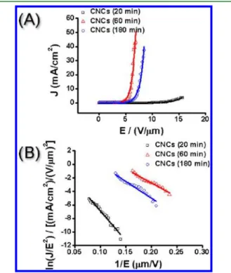
We select two sets of representative samples, with C2H2flow
rates of 11 and 2.7 sccm, to demonstrate the effects of the CNC growth time. For samples 18, 20, and 21 grown at 11 sccm, their EFE results are shown in Figure 8 and summarized in
Table 1. Among them, sample 20 shows the best performance. Its Eto,β, and J at 5 V/μm are 3.78 V/μm, 1852, and 1.64 mA/ cm2, respectively. In addition, it can emit a high density of electrons of 43 mA cm−2 at a relatively low 6.87 V μm−1. Sample 18 does not perform well because the CNC layer is relatively thin, as shown in Figure S7C in the Supporting Information. The CNCs in sample 21 are too crowded and wide in diameter, as shown in Figure S7G−I (Supporting Information). These probably cause a strong screening effect to
Figure 7. Variation of CNC (A) coil diameters and (B) layer thicknesses in samples 18, 20, and 21 against reaction time lengths.
Scheme 1. Proposed Growth Pathway of CNC on Graphite Foil
Figure 8.EFE properties of CNCs grown for different time lengths at 723 K anda C2H2flow rate of 11 sccm. (A) J−E curves and (B) FN plots. Samples 18, 20, and 21 were grown for 20, 60, and 180 min, respectively.
decrease the emission efficiency. In the cases of the flow rate 2.7 sccm, including samples 2, 22, and 23, the results are shown in Figure S9 and Table S4 in the Supporting Information. For these samples, their EFE performances increase with increased growth time. The observation is attributed to increased aspect ratios and emission sites as the growth time was increased. All of the results discussed above suggest that the EFE properties could be optimized under a certain combination of CNC sizes and CNC layer thicknesses. In this investigation, when a C2H2
flow rate of 11 sccm was used to grow the CNCs, the products grew fast and long to result in better performances.
As discussed above, varying the carrier gas flowed into the reactor during the CVD affected the product morphology greatly. Also, it was found that H2was an essential component
to assist the CNC formation. However, a concentration of H2
restricted the CNC growths probably owing to the passivation of the K surface by hydrides. As shown in Figure S4 (Supporting Information), CNCs (sample 2), curved NWs (sample 13), and C particles (sample 14) were grown by using H2(20 sccm), H2(30 sccm), and Ar (20 sccm), respectively. Their EFE results are shown in Figure S10 (Supporting Information) and summarized in Table S5 (Supporting Information). Among them, as expected, 14 does not emit electrons at thefields applied. Sample 2 performs much better than 13 does. Probably, 2, with more curly bodies, provides more emission sites.42We also demonstrated that CNCs could be grown under a broad range of C2H2 concentrations. As
shown in Figure 6, small diameter CNCs were synthesized at lowflow rates of C2H2, while large diameter CNCs were grown
at high concentrations of C2H2. Similar effects can be observed for the layer thicknesses of CNC layers. The EFE results of samples 2, 17, 18, and 19 are shown in Figure S11 (Supporting Information) and summarized in Table S6 (Supporting Information). Among them, 19 presents the best performance. Probably, relatively large amounts of long CNCs in 19 provide a high density of electron emission sites and enhance thefield
emission properties. The EFE measurements from three different sites on 19 show consistent results in Figure S12A in the Supporting Information. On the other hand, measuring two different samples of 20 (Figure S12B, Supporting Information) offers slightly different EFE performance. We expect the variations can be minimized by further process improvements.
■
CONCLUSIONSIn conclusion, we successfully synthesized CNCs with uniform morphology on bendable graphite substrates employing a Au and K bicatalyst assisted CVD process. The Au and K catalysts assisted the thermal decomposition of C2H2 to form CNCs
cooperatively. The optimized CNC growth parameters were achieved by using Au NPs 30−37 nm, coating a K layer for 20 min (evaporated at 423 K), providing streams of C2H2at 2.7−
22 sccm and H2at 20 sccm, and setting the growth temperature
at 723 K. By varying the growth time, the CNC lengths and the layer thicknesses could be controlled. The observations suggest that a tip-growth mechanism involving the Au NPs as the nucleation sites was in operation. In the reaction, the liquid-phase K metal assisted the decomposition of C2H2by lowering
the reaction temperature. We propose that acetylide and hydride intermediates were formed in the reaction. Further decomposition of the acetylide intermediates generated solid-phase C nucleated on the Au NPs and grown axially into NWs. The adhesion between the NW and the liquid-phase K particle would cause slower C atom deposition at the C−K interface, which is located at the inner curvature of the NW, than at the exposed C surface, the outer curvature. The phenomenon probably assists the NWs in curling into coils. Effects of varying the reaction conditions on the CNC growths are derived from the experimental data. They support the proposed bicatalyst enhanced tip-growth VLS mechanism. This is the second example of the bicatalyst system discovered so far.13 For possible EFE applications, the best performed sample provided an Etovalue of 3.78 V/μm and a field enhancement factor β of
1852. These are comparable to previously reported data summarized in Table 2. In addition, our sample revealed a current density, J, of 43 mA cm−2at 6.87 Vμm−1. This is twice as much as the other reported values. Presumably, our high density and uniformly shaped CNCs allow the emission of high electron currents. Consequently, these low-temperature grown CNCs on bendable graphite substrates enable many possible flexible EFE device applications.
Table 1. Summary of Effects of Growth Time and Lengths on EFE Properties of CNCs at 723 K and a C2H2Flow Rate
of 11 sccm
sample 18 20 21
reaction time (min) 20 60 180
Eto(V/μm) 8.31 3.78 4.46
J (mA/cm2) at 5 V/μm 1.73× 10⁻⁴ 1.64 0.16
β 873 1852 1546
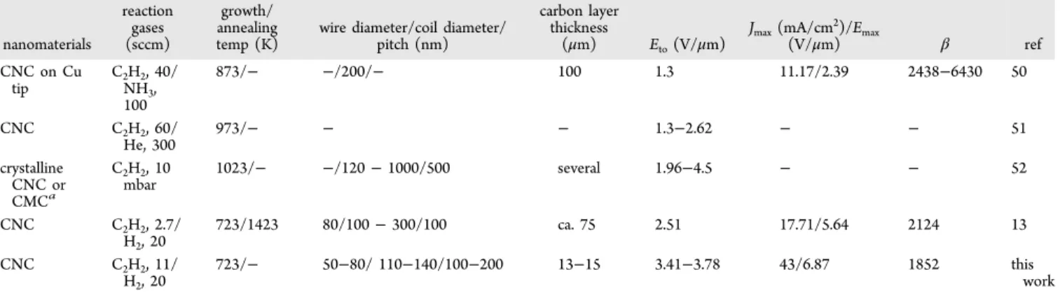
Table 2. Summary of Growth Parameters and EFE Characteristics of CNCs Reported in the Literature
nanomaterials reaction gases (sccm) growth/ annealing temp (K)
wire diameter/coil diameter/ pitch (nm)
carbon layer thickness
(μm) Eto(V/μm)
Jmax(mA/cm2)/Emax
(V/μm) β ref CNC on Cu tip C2H2, 40/ NH3, 100 873/− −/200/− 100 1.3 11.17/2.39 2438−6430 50 CNC C2H2, 60/ He, 300 973/− − − 1.3−2.62 − − 51 crystalline CNC or CMCa C2H2, 10 mbar 1023/− −/120 − 1000/500 several 1.96−4.5 − − 52 CNC C2H2, 2.7/ H2, 20 723/1423 80/100− 300/100 ca. 75 2.51 17.71/5.64 2124 13 CNC C2H2, 11/ H2, 20 723/− 50−80/ 110−140/100−200 13−15 3.41−3.78 43/6.87 1852 this work aCarbon microcoil: CMC.
■
ASSOCIATED CONTENT*
S Supporting InformationSEM images, tables, and figures of experimental data summaries. This material is available free of charge via the Internet at http://pubs.acs.org.
■
AUTHOR INFORMATIONCorresponding Author
*E-mail: [email protected].
Notes
The authors declare no competingfinancial interest.
■
ACKNOWLEDGMENTSWe are grateful to the support from the National Science Council, “Aim for the Top University Plan” of the National Chiao Tung University, and the Ministry of Education of Taiwan, the Republic of China.
■
REFERENCES(1) Coville, N. J.; Mhlanga, S. D.; Nxumalo, E. N.; Shaikjee, A. S. Afr. J. Sci. 2011, 107, 44−58.
(2) Chen, X.-Q.; Zhang, S.-L.; Dikin, D. A.; Ding, W.-Q.; Ruoff, R. S.; Pan, L.-J.; Nakayama, Y. Nano Lett. 2003, 3, 1299−1304.
(3) Antolini, E. Appl. Catal., B 2009, 88, 1−24.
(4) Che, J.-W.; Cagin, T.; Goddard, W. A. Nanotechnology 2000, 11, 65−69.
(5) Lin, C.-T.; Lee, C.-Y.; Chin, T.-S.; Xiang, R.; Ishikawa, K.; Shiomi, J.; Maruyama, S. Carbon 2011, 49, 1446−1452.
(6) Bower, C.; Zhu, W.; Shalom, D.; Lopez, D.; Chen, L.-H.; Gammel, P. L.; Jin, S. Appl. Phys. Lett. 2002, 80, 3820−3822.
(7) Koehne, J.; Chen, H.; Li, J.; Cassell, A. M.; Ye, Q.; Ng, H. T.; Han, J.; Meyyappan, M. Nanotechnology 2003, 14, 1239−1245.
(8) Choi, W. B.; Chu, J.-U.; Jeong, K.-S.; Bae, E.-J.; Lee, J.-W.; Kim, J.-J.; Lee, J.-O. Appl. Phys. Lett. 2001, 79, 3696−3698.
(9) Volodin, A.; Buntinx, D.; Ahlskog, M.; Fonseca, A.; Nagy, J. B.; Van Haesendonck, C. Nano Lett. 2004, 4, 1775−1779.
(10) Yang, S.; Chen, X.; Motojima, S. Carbon 2006, 44, 3352−3355. (11) Wang, L.-S.; Buchholz, D. B.; Li, Y.; Li, J.; Lee, C.-Y.; Chiu, H.-T.; Chang, R. P. H. Appl. Phys. A, Mater. Sci. Process. 2007, 87, 1−6.
(12) Jeong, H.-J.; Jeong, H.-D.; Kim, H.-Y.; Kim, J.-S.; Jeong, S.-Y.; Han, J.-T.; Bang, D.-S.; Lee, G.-W. Adv. Funct. Mater. 2011, 21, 1526− 1532.
(13) Liu, W.-C.; Lin, H.-K.; Chen, Y.-L.; Lee, C.-Y.; Chiu, H.-T. ACS Nano 2010, 4, 4149−4157.
(14) Venkatesan, N.; Yoshimitsu, J.; Ito, Y.; Shibata, N.; Takada, K. Biomaterials 2005, 26, 7154−7163.
(15) Klumpp, C.; Kostarelos, K.; Prato, M.; Bianco, A. Biochim. Biophys. Acta-Biomembr. 2006, 1758, 404−412.
(16) Jiang, F.; Wang, S.; Lin, J.-J.; Jin, H.-L.; Zhang, L.-J.; Huang, S.-M.; Wang, J.-C. Electrochem. Commun. 2011, 13, 363−365.
(17) Chang, J.-C.; Tzeng, Y.-F.; Chen, J.-M.; Chiu, H.-T.; Lee, C.-Y. Electrochim. Acta 2009, 54, 7066−7070.
(18) Hyeon, T.; Han, S.; Sung, Y.-E.; Park, K.-W.; Kim, Y.-W. Angew. Chem., Int. Ed. 2003, 42, 4352−4356.
(19) Chen, W.-Y.; Wang, L.-S.; Chiu, H.-T.; Chen, Y.-C.; Lee, C.-Y. J. Am. Soc. Mass Spectrom. 2004, 15, 1629−1635.
(20) Zhang, L.; Zhu, Y.-B.; Ge, C.-L.; Wei, C.; Wang, Q.-L. Solid State Commun. 2007, 142, 541−544.
(21) Lanjuan, W.; Chunzhong, L.; Feng, G.; Chuanxiang, Z. J. Alloys Compd. 2009, 473, 351−355.
(22) Sevilla, M.; Sanchís, C.; Valdés-Solís, T.; Morallón, E.; Fuertes, A. B. Electrochim. Acta 2009, 54, 2234−2238.
(23) Qi, X.-S.; Zhong, W.; Deng, Y.; Au, C.-T.; Du, Y.-W. Carbon 2010, 48, 365−376.
(24) Tang, N.; Zhong, W.; Au, C.; Yang, Y.; Han, M.; Lin, K.; Du, Y. J. Phys. Chem. C 2008, 112, 19316−19323.
(25) Jian, X. A.; Jiang, M.; Zhou, Z. W.; Yang, M.-L.; Lu, J.; Hu, S.-C.; Wang, Y.; Hui, D. Carbon 2010, 48, 4535−4541.
(26) Nitze, F.; Abou-Hamad, E.; Wagberg, T. Carbon 2011, 49, 1101−1107.
(27) Neng-Kai, C.; Shuo-Hung, C. Carbon 2008, 46, 1106−1109. (28) Yang, S.; Chen, X.; Kikuchi, N.; Motojima, S. Mater. Lett. 2008, 62, 1462−1465.
(29) Kawaguchi, M.; Nozaki, K.; Motojima, S.; Iwanaga, H. J. Cryst. Growth 1992, 118, 309−313.
(30) In-Hwang, W.; Chen, X. Q.; Kuzuya, T.; Kawabe, K.; Motojima, S. Carbon 2000, 38, 565−571.
(31) Amelinckx, S.; Zhang, X.-B.; Bernaerts, D.; Zhang, X.-F.; Ivanov, V.; Nagy, J. B. Science 1994, 265, 635−639.
(32) Bandaru, P. R.; Daraio, C.; Yang, K.; Rao, A.-M. J. Appl. Phys. 2007, 101, 094307−4.
(33) Fang, X.-S.; Bando, Y.; Gautam, U. K.; Ye, C.; Golberg, D. J. Mater. Chem. 2008, 18, 509−522.
(34) Wu, H.-C.; Tsai, H.-Y.; Chiu, H.-T.; Lee, C.-Y. ACS Appl. Mater. Interfaces 2010, 2, 3285−3288.
(35) Wu, H.-C.; Tsai, T.-Y.; Chu, F.-H.; Tai, N.-H.; Lin, H.-N.; Chiu, H.-T.; Lee, C.-Y. J. Phys. Chem. C 2010, 114, 130−133.
(36) Wu, H.-C.; Hou, T.-C.; Chueh, Y.-L.; Chen, L.-J.; Chiu, H.-T.; Lee, C.-Y. Nanotechnology 2010, 21, 455601−4.
(37) Chang, I.-C.; Huang, T.-K.; Lin, H.-K.; Tzeng, Y.-F.; Peng, C.-W.; Pan, F.-M.; Lee, C.-Y.; Chiu, H.-T. ACS Appl. Mater. Interfaces 2009, 1, 1375−1378.
(38) Zhao, Q.; Gao, J.-Y.; Zhu, R.; Cai, T.-C.; Wang, S.; Song, X.-F.; Liao, Z.-M.; Chen, X.-H.; Yu, D.-P. Nanotechnology 2010, 21, 095701− 6.
(39) Tseng, Y.-K.; Huang, C.-J.; Cheng, H.-M.; Lin, I.-N.; Liu, K.-S.; Chen, I.-C. Adv. Funct. Mater. 2003, 13, 811−814.
(40) Hsieh, C.-T.; Chen, J.-M.; Lin, H.-H.; Shih, H.-C. Appl. Phys. Lett. 2003, 83, 3383−3385.
(41) Lin, H.-K.; Tzeng, Y.-F.; Wang, C.-H.; Tai, N.-H.; Lin, I.-N.; Lee, C.-Y.; Chiu, H.-T. Chem. Mater. 2008, 20, 2429−2431.
(42) Pan, L.; Konishi, O.; Tanaka, H.; Suekane, O.; Nosaka, T.; Nakayama, Y. Jpn. J. Appl. Phys. Part 1 - Regul. Pap. Brief Commun. Rev. Pap. 2005, 44, 1652−1654.
(43) Agarwal, S.; Sarada, B. Y.; Kar, K. K. Nanotechnology 2010, 21, 65601−5.
(44) Wang, L.-S. Ph.D. Thesis, National Chiao Tung University, 2006.
(45) Takagi, D.; Homma, Y.; Hibino, H.; Suzuki, S.; Kobayashi, Y. Nano Lett. 2006, 6, 2462−2465.
(46) Yuan, D. N.; Ding, L.; Chu, H. B.; Feng, Y. Y.; McNicholas, T. P.; Liu, J. Nano Lett. 2008, 8, 2576−2579.
(47) Kuzuya, C.; In-Hwang, W.; Hirako, S.; Hishikawa, Y.; Motojima, S. Chem. Vapor Deposition 2002, 8, 57−62.
(48) Okamoto, H.; Massalski, T. J. Phase Equilib. 1984, 5, 378−379. (49) Bonard, J. M.; Weiss, N.; Kind, H.; Stöckli, T.; Forró, L.; Kern, K.; Châtelain, A. Adv. Mater. 2001, 13, 184−188.
(50) Sung, W.-Y.; Ok, J. G.; Kim, W.-J.; Lee, S.-M.; Yeon, S.-C.; Lee, H.-Y.; Kim, Y.-H. Nanotechnology 2007, 18, 245603−5.
(51) Pan, L.-J.; Hayashida, T.; Zhang, M.; Nakayama, Y. Jpn. J. Appl. Phys. Part 2 - Lett. 2001, 40, L235−L237.
(52) Banerjee, D.; Jha, A.; Chattopadhyay, K. K. Appl. Surf. Sci. 2010, 256, 7516−7521.