9:30am-9:45am
THAI .4
GROWTH AND CHARACTERIZATION
OF InAsN ALLOYS
Jyh-Shyang Wang, Hao-Hsiung Lin, Li-Wei Sung and Guan-Ru Chen
Room 41 9, Department of Electrical Engineering,
National Taiwan Universiv, Taipei, Taiwan, R.
0,C.
Abstract
The growth of InAsN alloys on InP and InAs substrates by using gas source molecular beam epitaxy (GSMBE) and RF plasma nitrogen source is reported. The samples grown on InP substrates were 3-nm-thick InAsN quantum wells (QW's). The nitrogen composition determined using double crystal X-ray difiactometer (DXRD) is linearly dependent on the nitrogen flow rate. The incorporation of nitrogen decreases the PL emission energy of the QW's. Increase the nitrogen composition by one- percent causes a red-shift energy of 3 1 meV. The highest nitrogen composition obtained in this study is 5.9 %, and its 10K PL peak wavelength is as long as 2.6 pm (480 meV). The DXRD results also indicate that the satellite peak linewidths of InAsN QW's are narrower than those of InAs QW, which means that the incorporation of nitrogen can sharpen the interfaces of QW's because it results in smaller lattice mismatch. However, increase nitrogen composition also degrades both the DXRD linewidths and the PL intensity. It suggests the existence of the residual strain or immiscibility introduced by the small diameter nitrogen atoms seated on arsenic sites. For InAsN grown on InAs substrates, the incorporation efficiency of nitrogen is much lower than that of InAsN grown on InP substrates. Compressive strain in InAsN on InP substrate could enhance the incorporation of nitrogen.
I. Introduction
Low nitrogen content zincblende 111-V alloys have received much attention in the past few years because of the huge bowing parameters induced by the large differences in atomic sizes and electronegativities of N and As (1-3). Besides the device applications on long- wavelength laser diodes (2, 3), theoretical approach has also been motivated to understand the huge bowing parameter and also to ascertain the semiconductor or semimetal nature of these alloys (4-6). Among these mixed group V alloys, InAsN alloy could be a very promising material for mid-infrared 2-5 pm optoelectronic devices. Recently, we had demonstrated a 2.2 pm InAs/InGaAs/InP highly strained multi-quantum well laser grown by gas- source molecular beam epitaxy (7). Using InAsN to replace InAs can ease the critical thickness limitation on the quantum well because of its small lattice constant, and can also further reduce the band gap energy of the quantum well because of its huge bowing effect. These two features reveal the possibilities of pushing the wavelength of lasers on InP substrates to longer infrared range. However, there are only limited studies on this alloy so far (8-12). In this paper, we report the GSMBE growth and characterization of InAsN/ InGaAsP MQW's on InP substrates and InAsN bulk layers on InAs substrates.
11. Experiment
The samples were grown on (100) InP and (100) InAs substrates using a VG V-80H GSMBE system. Besides the element In and Ga sources and thermally cracked ASH, and
0-7803-6320-5/00/$10.0002000
IEEE
549PH, sources, an EPI UNI-bulb RF plasma source was used to generate active N species. The RF power for these growths was kept at 120 W for the InAsN QW structures grown on InP substrates. After thermally cleaning the InP substrate at 500 "C under P, flux, a 0.5-pm-thick In,, 75Ga, 25Aso 53Po 47 layer lattice-matched to InP substrate was firstly grown as a buffer layer at a growth rate of 2 p&. High-brightness mode N, plasma was then ignited for the subsequent MQW growth. The MQW structure is comprised of 20 or 30-nm-thick In, 75Ga, 2sAs, 53P047 barriers and 3-nm-thick InAsN wells. The growth rate of
InAsN well was 1.5 p&. For studying the growth conditions, the range of growth temperature and A s h flux ratio were changed from 340 to 430°C and 1 to 3, respectively. And the range of nitrogen flow rate was changed from 0.2 to 1.4 sccm, whose corresponding beam equivalent pressure (BEP) was from 1 to 6 x l o 5 mbar. To control the illumination of nitrogen species, a mechanical shutter in front of the plasma source was used. However, there were no growth interruptions at the hetero- interfaces of the QW structures. The RF power was tumed off immediately after finishing the QW growth. Finally, a 0.1-pm-thick InP cap layer was overgrown on the MQW. The detailed growth conditions are summarized in Table 1.
Typical flow rate fluctuation was within 0.1 sccm.
For InAsN samples grown on (100) InAs substrates, The plasma power was from 200W to 500W. The growth temperature was 470 "C, and the As/In flux ratio was -3. The growth rate of InAsN layers was 1.5 pm/hr. The structure includes a 0.3-pm-thick InAs buffer layer, a 0.2- pm-thick InAsN layer, and a 0.1-pm-thick InAs cap layer.
A mechanical shutter was used to control the irradiation of nitrogen beam during the growth. Detailed growth conditions are summarized in Table2.
The nitrogen compositions of InAsN quantum wells were determined by fitting the DXRD spectra using a commercial dynamic simulation software RADS. The optical quality was evaluated using PL measurements. The 488 nm line of an argon laser was used as the excitation source and a closed cycle helium cryostat was used for low temperature measurements. The signal was detected using a liquid nitrogen cooled InSb photodiode with a Hamamatsu P3357-02 preamplifier.
Table 1: Growth conditions and nitrogen composition of InAsN QW's on InP substrates.
substrate peak, which indicates the reduction of lattice mismatch due to the incorporation of nitrogen. Note that the satellite peaks of InAsN /InGaAsP MQWs samples (C822, C823, and C824) are sharper than those of InAsAnGaAsP MQW sample (C82 1) showing that flatter hetero-interfaces are achieved in InAsNhnGaAsP samples due to their smaller lattice mismatch. On the other hand, it was also found that the satellite peaks broaden in spite of
the decreasing lattice-mismatch as the nitrogen flow rate increases in these InAsN MQW's. The degradation on the crystal quality might depend on the miscibility gap of InAsN materials. The nitrogen composition determined from the DXRD spectra as a function of nitrogen flow rates is plotted in Fig. 2. As can be seen, the nitrogen was roughly linearly incorporated into the solid by increasing the nitrogen flow rate.
Sample Number N,Flow Growth A s h Nitrogen
Number of periods rate Temperature ratio composition N, flow
(sccm)
("C)
(S-) 6 2 00 C82 1 10 0 400 2 0 C823 10 0.70 400 2 0.035 r C824 10 1.40 400 2 0.059 C827 4 0.43 430 2 0.022 C828 4 0.43 400 2 0.025 C829 4 0.43 370 2 0.027 C830 4 0.43 340 2 0.033 C832 4 0.43 400 3 0.013 C822 10 0.35 400 2 0.011 9 2.5
0 35 c-
0 70 140 Boo0 -4oo0 2000 0 2 mC83 1 4 0.43 400 1 0.028 Diffraction Anglee (arc-second)
Fig. 1 Double crystal X-ray difiaction (DXRD) spectra of 10-periods InAsNhnGaAsP MQWs grown at different nitrogen flow rates.
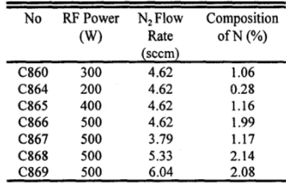
Table 2: Growth parameters and nitrogen compositions of InAsN alloys on InAs substrates
No RF Power N, Flow Composition
(W) Rate of N (%) (sccm) C860 300 4.62 1.06 C864 200 4.62 0.28 (2865 400 4.62 1.16 C866 500 4.62 1.99 C867 500 3.79 1.17 C868 500 5.33 2.14 C869 500 6.04 2.08
111. Results and Discussions 0 0 0 2 0 4 06 0 8 1 0 1 2 1 4 1 6
Flow rate of Nitrogen (sccm)
A. InAsN quantum wells grown on InP substrates Fig. 1 shows the DXRD spectra of 10-periods InAsN/ InGaAsP QW structures grown at different nitrogen flow rates. The well and barrier widths were 3 nm and 20 nm, respectively. As can be seen, increasing the nitrogen flow rate shifts the envelope of the satellite peaks toward the
Fig. 2 Nitrogen composition determined from DXRD
spectra as a function of nitrogen flow rates.
The 10 K PL spectra of the annealed InAsNAnGaAsP QW's are shown in Fig. 3. Detailed annealing procedures and effects were described in Ref 12. As can be seen, the
550
PL peak energy decreases with increasing nitrogen composition. This result indeed confirms the bowing effect due to the incorporation of nitrogen. However, the integrated PL intensity linearly degrades with increasing nitrogen composition, and the full width at half maximum (FWHM) also shows the similar behavior. In general, the more the N atoms incorporated into I d s , the worse the sample crystallinity, and the weaker the PL intensity. The degradation is due to the residual strain or immiscibility introduced by the small diameter nitrogen atoms seated on
arsenic sites. All of the behaviors are similar to those reported previously for InGaAsN system (1 -3,13- 16). In Fig. 3, sample C824, whose luminescence before annealing is not detectable, shows a 10K PL peak wavelength of -2.6 pm (480 meV). To the best of our knowledge, it is the longest inter-band transition wavelength of MQW's grown
on InP to date. From Fig. 3, it is found that the relationship between the PL emission energy and the nitrogen composition is close to linear. One percent increase in the nitrogen composition causes a red-shift of 31 meV on the 10K PL peak energy. This result is close to the composition versus bandgap relation reported by Naoi et. al. (9), though their InAsN were grown on GaAs by using MOCVD.
0.40 0.45 0.50 0.55 0.60 0.65 0.70
Energy (eV)
Fig. 3 10 K PL spectra of the annealed InAsNhGaAsP QWS
B. InAsN grown on InAs substrates
Fig. 4 shows the (400) DXRD spectra of the InAsN epilayers grown on InAs substrates. The thick curves are experimental results, while the thin curves are results of curve fitting using dynamic simulation software (RADS).
The fitted nitrogen contents are summarized in Table 2. Beside the (400) plane, the DXRD spectra of ( 5 11) plane were also measured. The lattice mismatches of lattice constant parallel to the growth plane calculated from these results are around the range of I O 4
-
lo". It confirms that these InAsN films are coherently grown on InAs substrates. The clear fringes on the experimental curves, as can beseen in Fig. 4, indicate that the InAsN layers are with good structural quality. The highest nitrogen content obtained in this study is 2.14%.
C . . . . I . . * . I . . . . l . . . . I . . . . I . . . . ~
Diffraction Angle 0 (arc-second)
I .
-1WO -500 0 500 1000 1500 2WO
Fig.4 Double crystal X-ray spectra of InAsN alloys on
InAs substrates.
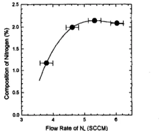
Fig. 5 shows the nitrogen composition as a hnction of plasma power with the nitrogen flow rate kept at 4.62 sccm. The composition linearly increases as the plasma power increases. Fig. 6 shows the relationship between the nitrogen composition and the nitrogen flow rate with the plasma power kept at 500W. As can be seen in the figure, the composition saturates approximately at 2.1% when the nitrogen flow rate reaches 5.3 sccm. Further increase the nitrogen flow rate results in slight decrease on the composition. This behavior is due to the degradation of plasma dissociation rate at high nitrogen flow rate (17). After comparing these flow rate and plasma power data with those for growing InAsN QW on InP substrates, it is found that the incorporation of nitrogen into InAsN grown on InAs substrate is much more difficult than into InAsN grown on InP substrates. Note that the plasma power for growing InAsN QW on InP is only 120W, and the flow rate is from 0 to 1.4 sccm only. In order to rule out the structure effect on this huge difference on growth conditions, 3-nm-thick InAsN QW's were also grown on InAs substrates. The composition coincides to that for bulk InAsN on InAs substrates. This huge difference could
be due to the high compressive strain in InAsN QW grown on InP substrate, because the incorporation of nitrogen in this case can reduce the strain and thus the surface free energy.
0 100 200 300 400 500 600
Plasma Power (W)
Fig. 5 Nitrogen composition as a function of plasma power. The nitrogen flow rate was fixed at 4.62 sccm.
2.0
1
c
Flow Rate of \ (SCCM)
Fig. 6 Nitrogen composition as a function of nitrogen flow rate. The plasma power was fixed at SOOW.
IV. Conclusion
In summary, we have grown InAsNAnGaAsP QW's
on
InP substrate and InAsN on InAs substrate by RF plasma nitrogen source used GSMBE. For InAsNhGaAsP QWs, the nitrogen composition determined using double crystal X-ray difliacto-meter (DXRD) is linearly dependent on the nitrogen flow rate. The red-shift of PL emission due tonitrogen incorporation was observed. Increase the nitrogen composition by one- percent causes a red-shift energy of 3 1 meV. The highest nitrogen composition obtained in this study is 5.9 %, and its 10K PL peak wavelength is as long
as 2.6 pm (480 meV). The DXRD results also show that the satellite peak linewidths of InAsN QW's are narrower than those of InAs QW, which means that the incorporation of nitrogen can sharpen the interfaces of QW's because it results in smaller lattice mismatch. However, increase
nitrogen composition also degrades both the DXRD
linewidths and the PL intensity. It suggests the existence of the residual strain or immiscibility introduced by the small diameter nitrogen atoms seated on arsenic sites. For InAsN
grown on
InAs
substrates, the highest nitrogen composition obtained in this study is only 2.1 %.The incorporation efftciency of nitrogen is much lower than that of InAsN grown on InP substrates.Acknowledgements
This work was supported by the National Science Council of the Republic of China under Contract No. NSC 89- 2215-E-002-034.
Reference
1. M. Kondow, K. Uomi, T. Kitatani, S. Watahiki, and Y. Yazawa, J. Crystal Growth 164,175 (1996).
2. M. Kondow,
T.
Kitatani, S . Nakatsuka,M.
C. Larson, K.Nakahara, Y. Yazawa, M. Okai, and K. Uomi, IEEE J.
Select. Topics Quantum Electron. 3 , 7 19 (1997). 3. W. G. Bi and C. W. Tu, Appl. Phys. Lett. 72, 1161 (1998).
4. S. Sakai, Y. Ueta, and Y. Teauchi, Jpn. J. Appl. Phys., Part 1 32,4413 (1993).
5 . S. H. Wei and A. Zunger, Phys. Rev. Lett. 76, 664 (1996).
6. L. Bellaiche, S. H. Wei. and A. Zunger, Phys. Rev. B 54, 17568 (1996).
7. J. S. Wang, H. H. Lin, and L. W. Sung, IEEE J. Quantum Electron. 34, 1959 (1998).
8. Y. C. Kao, T. P. E. Broekaert, H. Y. Liu, S. Tang, I. H. Ho, and G. B. Stringfellow, Mater. Res. Soc. Symp. Proc. 423,335 (1 996).
9. H. Naoi, Y. Naoi and S. Sakai, Solid-state Electronics 41, 319 (1997).
10. T. Yang, S. Nakajima, and S. Sakai, Jpn. J. Appl. Phys., 36, L320 (1997).
11. R. Beresford, K. S. Stevens, and A. F. Schwartzman, J. Vac. Sci. Technol. B 16(3), 1293 (1998).
12. J. S. Wang and H. H. Lin, 3. Vac. Sci. Technol. B 17, 1997 (1 999).
13. S. Sato, Y. Osawa and T. Saitoh, Jpn. J. Appl. Phys., 36, 267 1 (1 997).
14. H. Saito, T. Makimoto, and N. Kobayashi, J. Crystal Growth 195,416 (1998).
15. C. Jin, Y. Qiu, S . A. Nikishin, and H. Temkin, Appl. Phys. Lett., 74,3516 (1999).
16. H. P. Xin and C. W. Tu, Appl. Phys. Lett., 72, 2442 (1998).
17. D. Voulot, R. W. McCullough, W. R. Thompson, D.
Burns, J. Geddes, G. J. Cosimini, E. Nelson, P. P. Chow, and J. Klaassen, J. Crystal Growth, 2011202,399 (1999).