國立交通大學
電子工程學系電子研究所
碩士論文
閘極高介電值絕緣層穿隧電流的模擬
Modeling of Tunneling Currents in High-K Gate Stacks
研究生:張華罡 Hua-Gang Chang
指導教授:陳明哲 Prof. Ming-Jer Chen
閘極高介電值絕緣層穿隧電流的模擬
Modeling of Tunneling Currents in High-K Gate Stacks
研究生:張華罡 Hua-Gang Chang
指導教授:陳明哲 Prof. Ming-Jer Chen
國立交通大學
電子工程學系電子研究所
碩士論文
A Thesis
Submitted to Department of Electronics Engineering &
Institute of Electronics
College of Electrical and Computer Engineering
National Chiao Tung University
in Partial Fulfillment of the Requirements
for the Degree of
Master of Science
in
Electronics Engineering
September 2010
Hsinchu, Taiwan, Republic of China
I
閘極高介電值絕緣層穿隧電流的模擬
研究生:張華罡 指導教授:陳明哲博士 國立交通大學 電子工程學系電子研究所摘要
因為高介電值絕緣層可以達到抑制閘極漏電流的目的,所以傳統的閘極氧化介 電層正逐漸被高介電值絕緣層所取代。雖然高介電值絕緣層的電性特性已經被發 表過了,但是高介電值絕緣層的物理基礎模型還沒有被完全的研究透徹。 在此論文中,建立一個針對 n 型金氧半電晶體的高介電值絕緣層電子穿隧模 型。針對高介電值絕緣層穿隧電流的機制將會逐步地一一介紹。首先我們用複矽 晶閘極單氧化層的簡易結構來解釋其操作原理。這個原理包含四個關鍵的參數: 反轉層的電荷密度,電子對於氧化層/矽介面的撞擊頻率,WKB 的傳輸機率,以 及反射波的修正因子。 接著,將只有一層的閘極絕緣層模型擴展到適用於高介電值絕緣層的二層結 構。對於電子穿隧模型變數的影響將會詳細地分析。並且在對於高介電值絕緣層 穿隧電流的模擬及量測上得到卓越的符合。重要的是,穿隧變數以及能帶圖能夠 相應的得到,這可以更加地了解電子在高介電值絕緣層中的閘極穿隧機制。II
Modeling of Tunneling Currents in High-K Gate Stacks
Student: Hua-Gang Chang Advisor: Prof. Ming-Jer Chen Department of Electronics Engineering and Institute of Electronics
National Chiao Tung University
Abstract
Because the high-K stacks could achieve the target in suppressing the gate leakage current, conventional SiO2 gate dielectrics is being gradually replaced by high-K
materials. Although electrical characteristics have been demonstrated for high-K stacks, a physically based model of tunneling currents through high-K stacks has not been thoroughly investigated.
In this thesis, an electron tunneling model of high-K stacks will be constructed for nMOSFETs. The mechanisms responsible for the tunneling current will be introduced step by step. First, we explain the operational principle in a simplified framework of one oxide layer with poly gate. This principle comprises four key physical parameters: the inversion layer charge density, the electron impact frequency on SiO2/Si interface,
the WKB transmission probability, and the reflection correction factor.
Then, the structure to treat the case of only one gate dielectric layer model is augmented to that of a two-layer high-K stacks. The impact of the model parameters on the electron tunneling is analyzed in detail. Excellent agreements between simulated and measured tunneling currents are achieved. Importantly, the tunneling parameters and energy band diagrams are obtained accordingly, leading to a better understanding of the tunneling mechanism of electrons in high-K gate stacks.
III
誌
謝
首先,要感謝指導教授陳明哲博士的細心教導。當初的我對於半導體物理毫 無基礎,即便如此老師依然持續給予我鼓勵、支持。此外在研究方面老師的指導 更是令我獲益良多。 接著要感謝的是實驗室的各位,在這二年的相處裡我過得相當有趣、充實。 其中,特別是許智育學長,由於他的指導及幫助,我的研究才漸漸步入正軌。最 終論文能夠完成,也是學長不厭其煩地指點之故。研究所的二年裡因為有大家的 陪伴,讓我的回憶裡充滿著歡笑、溫暖。 最後感謝我的家人。我的任性給家人們帶來了許多的困擾、麻煩,但是他們 以包容以及諒解來支持著我。因為有他們的鼓勵和陪伴,我才能一步步往前邁 進,真心地感謝他們。
IV
Contents
Abstract (Chinese) ……….………..I
Abstract (English)………...………... II
Acknowledgement……… III
Contents……… IV
Figure Captions ………..V
Chapter 1 Introduction
1.1 Origin………...….1
1.2 Arrangement of this Thesis………...1
Chapter 2 Experimental
………3
Chapter 3 Physical Model of Direct Tunneling across Oxide
Dielectric
3.1 Critical Factors……….4
3.2 Inversion Layer Charge………4
3.3 Impact Frequency……….………5
3.4 Transmission Probability………..6
Chapter 4 Simplified Method to Calculate Subband Energy
…..10
Chapter 5 Tunneling Model for High-K Gate Stacks
5.1 MOS Electrostatics……….13
V
5.2 WKB Probability for High-K Stacks………....…..14
5.3 Correction factor for High-K Stacks………..16
Chapter 6 Application and Discussion
……….…...17
Chapter 7 Conclusion
………..………20
References
………..22
VI
Figure Captions
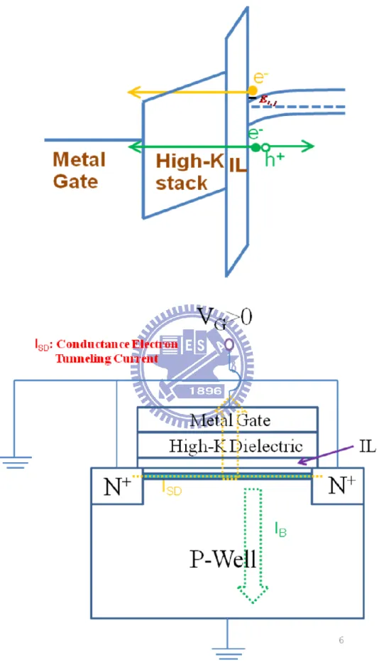
Fig. 1. The gate leakage current is composed of conductance electron
tunneling current (I
SD) and valence hole current (I
B)…..…24
Fig. 2. Gate current separation shows the conductance electron
tunneling current is dominant the gate leakage current in
inversion region………25
Fig. 3. Measured gate current versus gate voltage for T = 373K and
T=300K of (a) TaC/HfSiON/IL gate stacks and (b)
TiN/HfO
2/IL gate stacks of nMOSFETs………..…26
Fig. 4. Comparison of simulated (line) gate current change of T = 373K
with respect to T = 300K versus gate voltage with our
measured current (scatters)………...…27
Fig. 5. The energy band diagram schematically shown for the n
+poly/
SiO
2/p-substrate system………...………..28
Fig. 6. The measured gate current versus gate voltage and its fitting for
n
+poly gate MOSFETs………...29
VII
MOSFETs………..30
Fig. 8. The energy band for the metal gate/high-K/interface layer/Si
substrate system diagram for two level high-K stacks……..31
Fig. 9. Three different cases for electron tunneling in varying gate
voltage………32
Fig. 10. The demonstration of three different tunneling regions……….33
Fig. 11. The influence of (a)
ILand (b)
high Kon the calculated gate
tunneling current………34
Fig. 12. The influence of (a)
mILand (b)
mhigh Kon the calculated gate
tunneling current………....35
Fig. 13. The influence of (a)
tILand (b)
thigh Kon the calculated gate
tunneling current………36
Fig. 14. The influence of (a)
ILand (b)
high Kon the calculated gate
tunneling current………37
Fig. 15. The influence of (a)
Nsuband (b)
metalon the calculated gate
VIII
Fig. 16. The fitting results by our model in comparison with the measured
tunneling current in the literature [7]. The tunneling
parameters are the same as those in [7]……….…39
Fig. 17. The measured capacitance versus gate voltage for two different
gate stacks. And it is also shown the fitting lines…………..40
Fig. 18. The measured drain currents versus gate voltage for (a)
TaC/HfSiON/IL and (b) TiN/HfO
2/IL gate stacks………….41
Fig. 19. Comparison of the measured and calculated gate currents versus
gate voltage for (a) TaC/HfSiON/IL and (b) TiN/HfO
2/IL gate
1
Chapter 1 Introduction
1.1 Origin
Ultrascaled metal oxide semiconductor (MOS) technology requires the replacement of conventional SiO2 gate dielectrics by high-K materials. The high-K gate stacks are
able to reduce the gate leakage current. Besides, in order to shrink MOSFET devices into the deep-submicrometer regime, there are two factors taken into account: One is the level of increasing channel dopants and the other is gate dielectric thickness reduction. Both lead to a significant increase of the surface electric field, this imposing high demands on the advanced technology and on the understanding of the device physics involved. The combination of extremely thin gate dielectric material and high channel doping level produces a sufficiently large silicon electric field to confine the mobile carriers.
The MOSFET gate oxide thickness is rapidly approaching the direct tunneling limit that ultimately leads to intolerably large standby power and impractical applications. Thus, high-K stacks exhibit lower gate tunneling current. Although electrical characteristics have been demonstrated for high-K stacks, a physically based modeling of tunnel current through high-K stacks has not been thoroughly investigated. Accurate characterization and modeling of high-K stacks in the tunneling regime is essential and crucial. The latter can provide more transparent understandings since it is made up of four key physical parameters: the inversion layer charge density, the electron impact frequency on interface, the WKB transmission probability, and specially, the reflection correction factor.
1.2 Arrangement of this Thesis
First of all, this thesis is organized based on the following arrangement. Chapter 2 is the discussion of current separation and temperature effect. In Chapter 3, a
2
physical model for electron direct tunneling current in poly-gate nMOSFETs with ultrathin gate oxides is derived. This model comprises four key physical parameters: the inversion layer charge density, the electron impact frequency on SiO2/Si
interface, the WKB transmission probability, and the reflection correction factor. In Chapter 4, in order to build a model of the high-K stacks electron tunneling current accounting for electron’s subbands in the quantized inversion layer explicitly, a simplified method to calculate the subband energies will be introduced. In particular, the proposed model points out that the calculated secondary subbands and beyond, despite occupying few electrons, indeed contribute substantially to the direct tunneling conduction due to lower effective barrier heights.
In addition, high-K dielectrics with equivalent oxide thickness but larger physical thickness have been investigated as a replacement for SiO2 one. An ultrathin
interfacial oxide layer is required and can be formed during the fabrication below the high-K materials to improve interface quality with Si. Thus, accurate characterization and modeling of high-K gate stacks for the electron tunneling current is essential. The model built in Chapter 2 will be augmented to incorporate the high-K stacks. The process of parameter adjustment will be detailed in Chapter 5.
In Chapter 6, a physical model of tunneling currents through high-K gate stacks will be described. The effect of the model parameters on the electron tunneling will be analyzed in detail. Excellent agreements between simulated and measured tunneling currents will be demonstrated for MOSFETs with high-K gate stacks. We will also quote the literature value for comparison. The model is shown to enable in-depth understanding of the tunneling mechanisms.
Finally, Chapter 7 is the dedicated to conclusion of the proposed electron tunneling model as well as the potential application of the model.
3
Chapter 2 Experimental
Fig.1 shows the bias condition and gate leakage current separation, the gate leakage current is composed of conductance electron tunneling current (ISD) and valence hole
current (IB). Fig.2 displays that the conductance electron tunneling current is
dominant the gate leakage current in high gate voltage. Therefore the gate leakage current can be described by conductance electron direct tunneling model in inversion region.
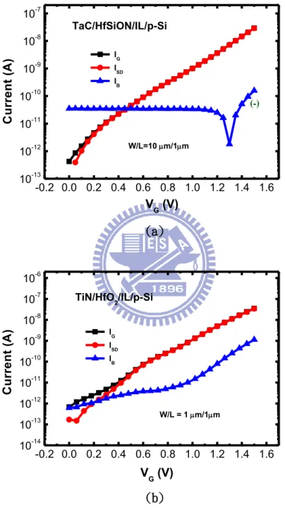
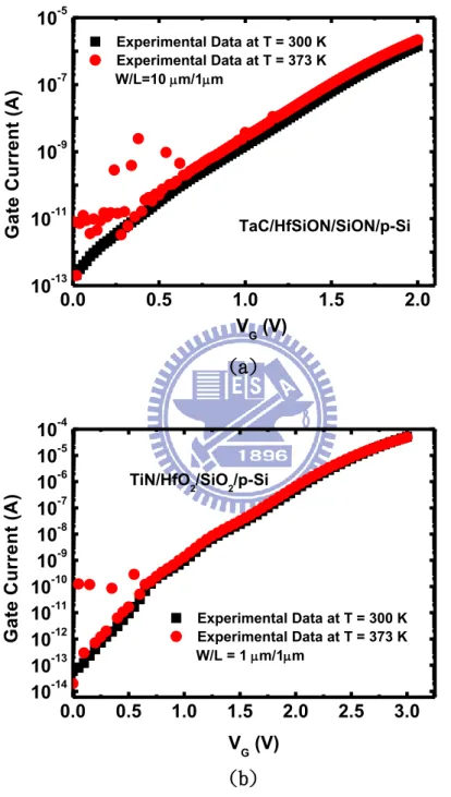
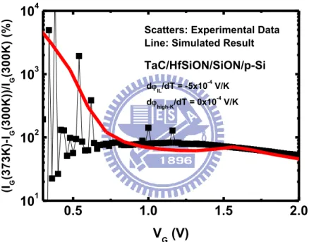
To determine the mechanisms responsible for gate current, the gate current are also measured at 1000C, as shown in Fig. 3.Gate current measurement in high temperature (100oC) was also done for determing the dominant physical mechanisms of the gate current, as shown in Fig. 3. The measured gate current is insensitive with temperature in inversion region. This indicates that the direct and F-N tunneling mechanisms dominate the transmission process of gate current in inversion region. Moreover, the measured gate current change of T = 373K with respect to T = 300K versus gate voltage of Fig. 3(a) is shown in Fig. 4.
The simulated gate current change of T = 373K with respect to T = 300K versus gate voltage is also presented in Fig. 4 and then a good reproduction of experimental data is done. This specific characteristic of temperauture effects on gate current over the gate voltage can serve as the evidence that the physical mechanisms of the mesured gate current are dominated by direct and F-N tunneling. The trap-assist-tunneling is neglected in this study by the support of the temperature characteristic of our mesured gate current. Hence, in this work, considering the direct and F-N tunneling only in fitting gtae curent of the metal gate high-k deice is reasonable.
4
Chapter 3 Physical Model of Direct Tunneling across Oxide
Dielectric
3.1 Critical Factors
First of all, we explain the fundamental principle of electron direct tunneling in a n+poly-SiO2-p-substrate structure, and expand it to include the case of high-K stacks.
We employ quantum mechanical calculations for the inversion layer in p-type substrate along with a modified WKB approximation for the transmission probability across the gate oxide [1], [2].
The direct tunneling electron current from each subbands can be formulated in a similar way. Electron current density contributed by j -th subband for two or four fold valleys with energy E to EdE can be written as
, ( ) ( ) ( )
i j j t
dJ E qf g E P E dE
(3-1) where
q is the elemental charge; ( )
g E is the inversion layer charge density per unit area magnitude of energy E
associated with j -th subband;
j
f is the impact frequency of electron’s wave packet on SiO2/Si interface; and ( )
t
P E is the transmission probability through SiO2 layer.
Then we will make a physical description of the key parameters above.
3.2 Inversion Layer Charge
5
inversion charge increment,
2 2
E dE
inv E D e D e
dN
g F E dE g F E dE (3-2) where F E indicates Fermi-Dirac distribution function of electrons and e
F Ee
associated with conduction electrons is 1 1/
exp
Ef E
/k TB
. In addition, g2 Drepresents density of states per unit area over electron energy for 2DEG (2-dimensional electron gas). The m is the density of states effective mass d
2 2 d D m g (3-3) From the variation of inversion-layer charge, g E could be obtained accordingly,
2
inv D e dN g E g F E dE (3-4)3.3 Impact Frequency
The impact frequency f can be expressed as, j
1 1 2 0 2 2 2 , , ( ) j z ox j z i i j si Si q F dz f m E v z
(3-5)where zj is the classical turning point at the j-th subband edge and m means the z i,
effective mass along 100 direction for two or four fold valleys. The field strength of oxide is designated as F . Furthermore, ox vsi( ) is the interface-normal velocity z
of electron wave packet, which can be written as
2( , ( )) ( ) i j si z E qV z v z m (3-6)
Here E is the quantized energy level of the j -th subband for two or four fold i j,
6
Thus, we are able to get quantized energy along z-direction or 100 direction in reciprocal space by using Sommerfeld-Wilson’s quantization rule :
2 3 1 2 3 1 3 4 2 2 , ox ox i j z Si q F j E m (3-7)
3.4 Transmission Probability
Before we discuss the transmission probability through SiO2 layer, the underlying
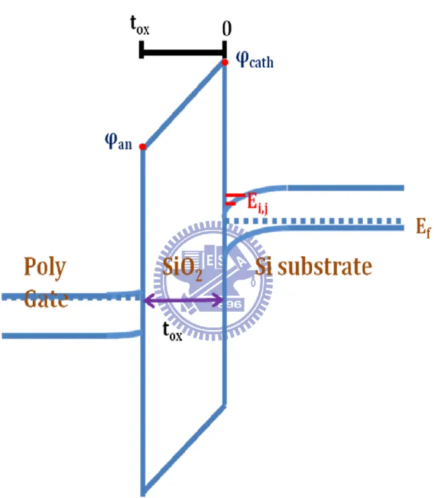
electrostatics must be made clear. The energy band diagram as shown in Fig. 5 is constructed for the n+poly/SiO2/p-substrate system. Under the inversion condition, it
is easy to write
G FB ox ox s poly
V V t F (3-8)
where VG means gate voltage, VFB represents flat-band voltage, and s and poly are the surface potential near the SiO2/p-substrate and SiO2/poly gate, respectively. In
addition, once the surface potential are quantified, then we can get the quasi Fermi level E from the following formula f
f s Bp E (3-9) where V g B A Bp N E k T N q ln (3-10)
where Bp is the potential difference between the quasi Fermi level
Ef /q
and conduction band
EC/q
in the charge neutrality range of p-substrate, and, k is B7
the Boltzmann’s constant.
Finally, based on the citation [3], P Et( ) can be modeled by
( ) ( ) ( )
t WKB R
P E T E T E (3-11)
where TWKB is the usual WKB tunneling probability valid for smooth varying
potential, and T is a factor corrected for the reflections due to the potential R
discontinuities:
0 0 3 3 2 2 2 2 2 4 2 3 ox ox t WKB t ox ox an cath ox T E z dz m E qV z dz m q F
( ) exp exp exp (3-12)where an is the barrier height for tunneling electrons with total energy E at anode
side (poly gate/SiO2 interface), and cath is that at cathode side (SiO2/p-substrate
interface). In this model, ox represents the SiO2/Si barrier height. The barrier height
for tunneling electrons can be described by
an ox q F tox ox E
(3-13)
cath ox E
(3-14) The total energy E consists of the transversal and longitudinal energies:
2 2 2 2 , x y i j t k k E E m (3-15) where m is the in-plane effective mass, t Ei j, is quantized energy in the out-of-plane direction .8
On the other hand, T is a justified factor concerning wavefunction’s reflection R
phenomenon occurring at SiO2/Si interfaces [4]. This correction factor has the
band-structure independent form. This relation is important in our model. T is R
obtained by considering reflections between the interfaces,
ox ox 2 2 2 2 ox ox 4 E+q F 4 E (E)= +q F ( ) ( ) ( ) ( ) ( ) ( ) ( ) ( ) si ox an si ox cath R si ox cath si ox an v t v v v T v E v v E t v (3-16) where vsi( )E and vsi(E+q Fox tox) are the group velocities of the electron incident
and leaving the oxide. The group velocity of electrons with energy E along 100 direction within the j-th subband at SiO2/Si interface is independent of E, as shown
below 2 E 0 , ( ) ( ) i j si si z E v v z m (3-17) The aforementioned vox(cath) and vox(an) are the magnitudes of the purely imaginary group velocities of electrons at the cathode and anode side within the oxide. Consequently, the imaginary group velocity which is dependent on E within oxide can be described by 2 1 an an ox ox ox d v dk m (3-18) This factor is significant, because if the electrostatic potential V x changes acutely ( )
with respect to position or the intensity of incident wave, it cannot be treated to be equal to that of reflection wave. In our model, we adopt a parabolic dispersion relation, 2 2 2 ( ) ox an ox ox ox k E qV x m (3-19)
9
Recalling (3-1), (3-4), (3-5), and (3-11), the tunneling current density contributed by the j-th subband with energy E ranging from E to infinity can be expressed i j,
2 = = , , ( ) ( ) ( ) ( ) ( ) j j j i j E i j j t E j D E e t J dJ E qf g E P E dE qf g F E P E dE
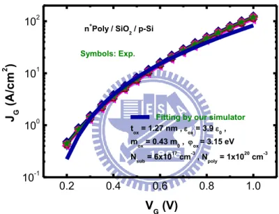
(3-20) The above electron direct tunneling model is verified by comparing experimental data from n+poly gate MOSFETs. The results are given in Fig. 6. It can be seen that excellent agreements between the experimental and simulated results are achieved. The drain currents versus gate voltage for n+poly gate/SiO2/p-substrate is shown inFig. 7, the threshold voltage Vth is obtained by the maximum trans-conductance method. In the calculation, the doping concentrations of poly gate and p-type substrate used (Npoly and Nsub) are 20
1 10 and 6 10 cm 17 3, respectively. The thickness of oxide t is extracted by C-V fitting. These parameters are all known when apply the ox
10
Chapter 4 Simplified Method to Calculate Subband Energy
In this chapter, we will introduce a simplified method to calculate the subband energies. The simplified method is to estimate the inversion and depletion charge densities. The band bending in depletion and inversion condition is also treated. In this work, we use the assumption to facilitate the model: The quantum confinement phenomenon of the MOS system can be treated in a triangular well approximation. The characteristic parameters of P-substrate under the inversion situation comprise of the followings:
Interfacial inversion charge Ninv;
Depleted space charge Ndepl;
Semiconductor surface potential or surface band bending s;
Band bending due to the depletion charge depl;
These parameters are interrelated by the following equation due to the law of electrostatics:
inv depl s
N N Q( ) (4-1)
Equation (4-1) states that the total charge per unit area Q below the MOS gate is the sum of the inversion electron charge Ninv and the depletion charge Ndepl:
0 s QM depl s Si qN z kT q (4-2)
From (4-2), the surface potential s is made up of the following components: the second term of the right side of (4-2) stems from the influence of inversion charge
inv
11
into the substrate, and the term depl due to the space charge Ndepl.
0 2 Si depl D depl N N q (4-3) The equivalent thickness of the quantum confined electron gas can be expressed as
QM i j i j i j F inv i j z
Z N, , E, E N , , (4-4)(4-4) reveals that the average of the subband widths z is weighted with the i j,
corresponding subband occupation factors N , then constituting the mean quantum i j,
mechanical channel width zQM. In this case, the wave functions are given by Airy
functions, and therefore the mean subband width z is i j,
2 2 3 , , , ( ) i j Si i j ox ox E z i j z zdz q E
(4-5) The energy eigenvalues E can be written by i j,
1 2 3 2 3 3 0 25 2 2 , . ox ox i j i Si q F j E m (4-6)where F is the oxide electric field and the index i determines the value of the ox
normal mass mi for two or four fold valleys. In addition, N can be derived from i j,
Fermi-Dirac statistics 2 1 , , , ( ) ( ) ln exp i j F i j di i j E i E E m N D E f E dE kT
(4-7) where D E is the density of states of the subband for two-dimensional gas and i( )( )
f E is the Fermi-Dirac occupation factor.
12
Although higher energy states share far less carriers, the other factor such as the transmission probability can be much larger than the ground state due to effective lower barrier heights for tunneling. Thus, the resulting tunneling current contains a substantial component from the secondary subbands and beyond. Besides the electron direct tunneling from the secondary subbands and beyond can be comparable to that from first subbands. Consequently, we can not ignore the contribution of the secondary and beyond to the electron tunneling current.
13
Chapter 5 Tunneling Model for High-K Gate Stacks
5.1 MOS Electrostatics
MOS electrostatics law is utilized to deal with the potential drops across the high-K gate stacks. The flat-band voltage for the poly gate and metal gate case can be written as
... log
metal sub G sub
FB
v
E KT N
V for metal gate
q q q q N (5-1) ... poly log G sub FB v E KT N V for gate q q N (5-2)
where metal is the workfunction of metal, and sub means electron affinity of p-substrate. Doping concentration of p-substrate is named Nsub. E (=1.12 eV) is G
band gap energy of silicon. Because there is high doping concentration in poly-silicon, the quasi-Fermi level approaches the conduction band edge for poly-silicon in energy band diagram.
By Gauss’ law we can get Vhigh K (potential drop across high-K dielectric) easily,
,
IL IL
IL high K IL
IL high K
high K high K high K
V F F F t V F t (5-3) The thickness of interfacial layer (IL) or high-K layer can be estimated by C-V method. Moreover, F and IL Fhigh K mean the electric field of IL and high-K
dielectric, respectively. The potential drop on IL (V ) is obtained by a self-consistent IL
calculation.
14
s VG VFB tIL FIL thigh K Fhigh K poly
(5-4) where thigh K Fhigh K and tIL FIL are the potential drop across the high-K dielectric
and interfacial layer, respectively. The n+-poly gate potential drop (poly) can be expressed as 2 2 2 IL IL poly Si poly F q N
In the metal gate case, it is also simple for modulating s. The formula is also suitable for metal gate case when deleting poly.
5.2 WKB Probability for High-K Stacks
The energy band diagram as shown in Fig. 8 is constructed for a two-layer high-K stack system. To calculate the tunneling probability, we have selected a modified WKB method with Pt TWKBTR , where TWKB is the usual WKB tunneling probability obtained for smooth varying potentials and T is the correction factor R
considering reflections from potential discontinuities. They can be treated as the most important part of electron tunneling model. The transmission probability P Et( ) not only goes across the interfacial layer (IL), but also the high-K dielectric [5], [6]. Therefore, TWKB has two portions needed to be treated, one is with regard to interfacial layer, and the other is on high-K dielectric:
3 3 2 2 2 2 2 (5-6) 4 2 4 2 3 , , , ( ) exp exp exp exp L R L R x WKB x x x IL high K x xIL IL an IL cath high K high K a
IL T E x dx x dx x dx m m q F
3 3 2 2 3 , , n high K cath high K q F 15
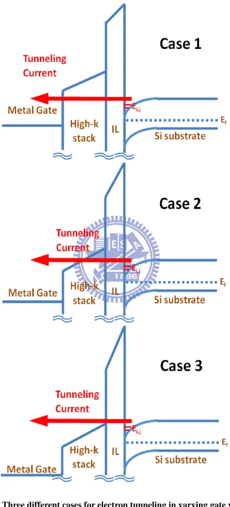
The index IL corresponds to the interfacial layer. The index high-K applies to the high-K dielectric. Now, this new equation can apply to high-K stacks, but it is still problematic in some conditions. The band diagram essentially varies with the change of the gate bias voltage. Consequently, Fig. 9 shows three different cases. Case 1 is normal situation that have been discussed above. Comparing Fig. 9, if a subband energy is lying between the two edges of high-K layer, namely case 2. When gate voltage gets larger, the subband energy of electrons is even higher than high-K edge which is located at interface of high-K dielectric and IL. In other words, the classification can be represented in the form of the following equations:
& ... 1 & ... 2 & ... 3 , , , , , ,
high K an high K cath
high K an high K cath
high K an high K cath
E E case E E case E E case (5-7) where, E means the total energy including the transversal and longitudinal energies. In case 2 and 3, they correspond to the following WKB approximation methods:
3 3 3 2 2 2 4 2 4 2 0 ... 2 3 3 , , , ( ) exp exp
IL IL an IL cath high K high K cath
WKB IL high K m m T E case q F q F 3 3 2 2 4 2 ... 3 3 , , ( ) exp IL IL an IL cath WKB IL m T E case q F (5-8)
Further, the potential energy for each edge of two layers could be calculated with the following equation,
, , , , , , IL cath IL IL an IL ILhigh K cath IL an IL high K
high K an IL an IL high K high K
E E V V (5-9)
16
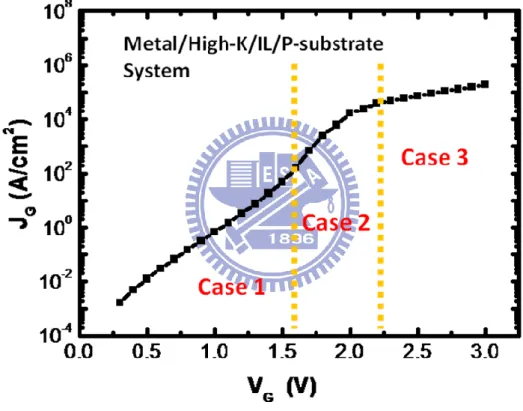
In case 2, electrons pass through IL by direct tunneling, but with F-N tunneling for high-K part. The behavior of electron F-N tunneling in high-K can appear in I-V characteristic. For example, Fig. 10 shows such a turning point when gate voltage increases to 1.6 V. As the gate current increases and exceeds the turning point different situation appears. Similarly, case 3 has only one kind of tunneling mechanism. Because the electrons have higher energy in case 3, they can go through IL by direct tunneling and surpass high-K layer immediately. The expression used for case 3 is like the only dielectric layer as discussed in Chapter 3. In case 3, the gate current increases with gate voltage.
5.3 Correction factor for High-K Stacks
In principle, there is a special TR which is in connection with high-K dielectric. But here, we only consider the reflection at the Si/IL interface in our model. The correction factor of interface reflection typically approaches unity for metal/high-K dielectric interface and for the interface of high-K gate stacks. The correction factors at the interface mentioned above can be neglected in our calculations. Therefore, T R
still maintains the original shape. The correcting T for high-K stacks is as follows: R
IL 2 2 IL 4 E (E)= , , ( ) ( ) ( ) ( ) si IL cath R si IL cath v v T v E v (5-10)
17
Chapter 6 Application and Discussion
We calculate the first and second subbands. The electron tunneling current from such two lowest subbands is almost the same as the actual tunneling current. Thus, for the computation time saving, the first and second subbands are considered only in this work. Although we have done many simplifications in the tunneling situation, the results are reasonable relation to the experimental measurement.
The tunneling model is constructed using an accurate description of electron quantization and a modified WKB method for tunneling through the barriers of high-K stacks. But the high-K stacks electron tunneling current simulator has a drawback: it could not simulate gate tunneling current correctly for the gate bias below threshold voltage. Our simulated model is based on direct tunneling mechanism; unfortunately, the direct tunneling is not dominant in subthreshold region. Although simulator can not work in subthreshold region, WKB approximation would show good agreements with the experiments once the gate bias is large enough. For this reason, the following discussion will be focused on the range of gate bias larger than the threshold voltage.
Finally, the new model for high-K stacks can be used to fit the results in literature about high-K tunneling. In addition, we also measure the I-V and C-V characteristics of devices with HfSiON and HfO2, and experimental reproduction has been
consistently achieved.
The influence of each model parameters on the gate tunneling current has been calculated as shown in Fig. 11-15. Here mIL and mhigh K are the effective mass for interfacial layer and high-K, respectively. The band offsets of IL and high-K relative to the conduction band of p-substrate are expressed as IL and high K , respectively.
18
Similarly, IL and high K mean the permittivity of IL and high-K, respectively.
From Fig. 11-15, high K determines the onset of case 2. The range that mhigh K
can have a significant effect concentrates on case 1 and 2, where the tunneling current is almost the same at high gate voltage. The influence of thigh K can also be seen,
especially its ability to determine the rage of case 2. As for high K , its influence is not
only on case 1 and 2 but also case 3, because high K will influence the electric field of IL indirectly. The parameters about IL impact the tunneling significantly in all cases. Finally, metal and Nsub can control the threshold voltage, which can help the calibration step in using our model. Briefly, In Fig. 11-15, different tunneling parameters have been varied with our simulator. The change of the tunneling current is seen clearly. Each parameter has different influences, and the results can help us fit data efficiently.
Moreover, we test the model by fitting experimental results in some open literature articles [4], [7]-[12]. This can verify the validity of the model for tunneling current simulation; for example, an excellent agreement between our simulated and the measured tunneling currents in the literature [7] has been obtained as shown in Fig. 16. The tunneling parameters used are those published [7], except several parameters not available such as doping concentrations.
We have also measured the gate tunneling current for two kinds of high-K stacks: TaC/HfSiON/IL and TiN/HfO2/IL. There is one thing needed to explain specially. IL
means interfacial layer, but it is not always formed by SiO2. In fact, the IL of our
device under test is SiON and SiO2 for HfSiON and HfO2, respectively. The measured
capacitance versus gate voltage for two different gate stacks is exhibited in Fig. 17. From C-V fitting method, the metal work function metal and p type substrate doping
19
concentration Nsub can both be obtained. Meanwhile, the effective oxide thickness (EOT) can also be determined. These parameters which are obtained from C-V fitting are the inputs to the gate tunneling current model. Moreover, from the drain currents versus gate voltage shown in Fig. 18, we can obtain threshold voltage Vth by the maximum trans-conductance method. The gate current fitting results for TaC/HfSiON/IL and TiN/HfO2/IL are shown in Fig. 19. It can be seen that for two
level high-K stacks, the experimental gate current can be fitted well. The high-K stacks tunneling simulator can apply to either metal gate or poly gate. The tunneling parameters and energy band diagram can be established via the data fitting. Furthermore, a better understanding of the gate tunneling mechanisms of electrons in high-K stacks can therefore be captured clearly.
20
Chapter 7 Conclusion
A physically based tunneling model is constructed using an accurate description of the electron quantization in the confined inversion-layer. This model contains a modified Wentzel–Kramers–Brillouin (WKB) method for tunneling through the barrier, including the effects of an ultrathin interfacial layer. The physical model of the electron tunneling through high-K stacks has been built up and experimental reproduction has been consistently achieved.
Our electron tunneling model is applied to high-K stacks. This model is easy to realize and computationally efficient. The data from the other tunneling models published in the open literature is also presented to confirm the accuracy of our model. From the model, the effect of high-K film will appear when the F-N tunneling begins to dominate in high gate voltage. As the gate voltage goes higher, because of the reduced barrier height of the high-K film, electrons will tunnel within the Fowler Nordheim regime instead of the direct tunneling regime. So it is important to find a high-K dielectric with a sufficient barrier height to reduce tunneling current in a wide range of gate voltages.
This model has evidenced its potential applications in enabling in-depth understanding of the different subbands in the confined inversion layer in affecting electron tunneling conduction. The high-K stacks tunneling simulator can apply to either metal gate or poly gate. The tunneling parameters and energy band diagram can be established by the data fitting. We can therefore capture the underlying gate tunneling mechanisms of electrons in high-K gate stacks.
But there are efforts needed to investigate for further, such the hole tunneling across the high-K gate stacks. Even the temperature effect may be significant and must be
21
taken into account. In addition, the electron tunneling model which was built in this thesis is focused on the inversion condition. Its extension to the accumulation may be needed.
22
References
1. L. F. Register, E. Rosenbaum, and K. Yang, “Analytic model for direct tunneling current in polycrystalline silicon-gate metal-oxide-semiconductor devices,” Appl.
Phys. Lett., vol. 74, no. 3, pp. 457-459, Jan. 1999.
2. K. N. Yang, H. T. Huang, M. C. Chang, C. M. Chu, Y. S. Chen, M. J. Chen, Y. M. Lin, M. C. Yu, S. M. Jang, D. C. H. Yu, and M. S. Liang, “A physical model for hole direct tunneling current in p+ poly-gate PMOSFETs with ultrathin gate oxides,” IEEE Trans. Electron Devices, vol. 47, no. 11, pp. 2161-2166, Nov. 2000. 3. N. Yang, W. K. Henson, J. R. Hauser, and J. Wortman, “Estimation of the effects of remote charge scattering on electron mobility of n-MOSFET’s with ultrathin gate oxides,” IEEE Trans. Electron Devices, vol. 47, no. 2, pp. 440-447, Feb. 2000.
4. F. Li, S. P. Mudanai, Y. Y. Fan, L. F. Register, and S. K. Banerjee, “Physically based quantum-mechanical compact model of MOS devices substrate-injected tunneling current through ultrathin (EOT ~ 1 nm) SiO2 and high-K gate stacks,”
IEEE Trans. Electron Devices, vol. 53, no. 5, pp. 1096-1106, May. 2006.
5. F. Li, Y. Y. Fan, L. F. Register, and S. K. Banerjee, “Compact model of MOSFET electron tunneling current through ultra-thin SiO2 and high-k gate stacks,” in
Device Res. Conf., Jun. 2003, pp. 47-48.
6. Y. Zhao and M. H. White, “Modeling of direct tunneling current through interfacial SiO2 and high-k gate stacks,” in Semicond. Device Res. Symp., Dec.
2003, pp. 468-469.
7. Y. T. Hou, M. F. Li, H. Y. Yu, and D. L. Kwong, “Modeling of tunneling current through HfO2 and (HfO2)x(Al2O3)1-x gate stacks,” IEEE Electron Device Lett., vol.
23
24, no. 2, pp. 96-98, Feb. 2003.
8. M. A. Quevedo-Lopez, S. A. Krishnan, P. D. Kirsch, H. J. Li, J. H. Sim, C. Huffman, J. J. Peterson, B. H. Lee, G. Pant, B. E. Gnade, M. J. Kim, R. M. Wallace, D. Guo, H. Bu, and T. P. Ma, “High performance gate first HfSiON dielectric satisfying 45nm node requirements,” in IEDM Tech. Dig., Dec. 2005, pp. 425-428.
9. R. G. Southwick, J. Reed, C. Buu, H. Bui, R. Butler, G. Bersuker, and W. B. Knowlton, “Temperature (5.6-300K) dependence comparison of carrier transport mechanisms in HfO2/SiO2 and SiO2 MOS gate stacks,” in IRW, Oct. 2008, pp.
48-54.
10. J. Coignus, C. Leroux, R. Clerc, G. Ghibaudo, G. Reimbold, and F. Boulanger, “Experimental investigation of transport mechanisms through HfO2 gate stacks in
nMOS transistors,” in Solid State Device Res. Conf. ESSDERC, Sept. 2009, pp. 169-172.
11. J. Coignus, R. Clerc, C. Leroux, G. Reimbold, G. Ghibaudo, and F. Boulanger, “Analytical modeling of tunneling current through SiO2-HfO2 stacks in metal
oxide semiconductor structures,” J. Vac. Sci. Technol. B, vol. 27, no. 1, pp. 338-345, Feb. 2009.
12. A. Campera, G. Iannaccone, and F. Crupi, “Modeling of tunneling currents in Hf-based gate stacks as a function of temperature and extraction of material parameters,” IEEE Trans. Electron Devices, vol. 54, no. 1, pp. 83-89, Jan. 2007.
24
Fig. 1. The gate leakage current is composed of conductance electron tunneling current (ISD) and valence hole current (IB).
25 -0.2 0.0 0.2 0.4 0.6 0.8 1.0 1.2 1.4 1.6 10-13 10-12 10-11 10-10 10-9 10-8 10-7 (-) IG ISD IB VG (V) C u rr e n t (A ) W/L=10 m/1m TaC/HfSiON/IL/p-Si (a) -0.2 0.0 0.2 0.4 0.6 0.8 1.0 1.2 1.4 1.6 10-14 10-13 10-12 10-11 10-10 10-9 10-8 10-7 10-6 IG ISD IB W/L = 1 m/1m TiN/HfO2/IL/p-Si VG (V) C u rr e n t (A ) (b)
Fig. 2. Gate current separation shows the conductance electron tunneling current is dominant the gate leakage current in inversion region.
26 0.0 0.5 1.0 1.5 2.0 10-13 10-11 10-9 10-7 10-5 TaC/HfSiON/SiON/p-Si G a te C u rr e n t (A ) VG (V) Experimental Data at T = 300 K Experimental Data at T = 373 K W/L=10 m/1m (a) 0.0 0.5 1.0 1.5 2.0 2.5 3.0 10-14 10-13 10-12 10-11 10-10 10-9 10-8 10-7 10-6 10-5 10-4
TiN/HfO2/SiO2/p-Si
Experimental Data at T = 300 K Experimental Data at T = 373 K W/L = 1 m/1m G a te C u rr e n t (A ) VG (V) (b)
Fig. 3. Measured gate current versus gate voltage for T = 373K and T=300K of (a) TaC/HfSiON/IL gate stacks and (b) TiN/HfO2/IL gate stacks of nMOSFETs.
27 0.5 1.0 1.5 2.0 101 102 103 104 dhigh-K/dT = 0x10-4 V/K dIL/dT = -5x10⁻⁴ V/K TaC/HfSiON/SiON/p-Si
Scatters: Experimental Data Line: Simulated Result
(I G (3 7 3 K )-I G (3 0 0 K )) /I G (3 0 0 K ) (% ) VG (V)
Fig. 4. Comparison of simulated (line) gate current change of T = 373K with respect to T = 300K versus gate voltage with our measured current (scatters).
28
Fig. 5. The energy band diagram schematically shown for the n+poly/SiO2/p-substrate system.
29 0.2 0.4 0.6 0.8 1.0 10-1 100 101 102 Symbols: Exp.
Fitting by our simulator
tox = 1.27 nm , ox = 3.9 0 , mox = 0.43 m0 ,ox = 3.15 eV Nsub = 6x1017 cm-3 , N
poly = 1x10 20 cm-3
n+Poly / SiO2 / p-Si
VG (V) J G ( A /c m 2 )
Fig. 6. The measured gate current versus gate voltage and its fitting for n+poly gate MOSFETs.
30 0.0 0.2 0.4 0.6 0.8 1.0 0.0 2.0x10⁻⁵ 4.0x10⁻⁵ 6.0x10⁻⁵ 8.0x10⁻⁵ 1.0x10⁻⁴ W = 10m L = 1 m I D ( A ) VD = 0.025 V Vth = 0.18655 V Symbols: Exp. VG (V) n+Poly / SiO 2 / p-Si
Fig. 7. The measured drain currents versus gate voltage for n+poly gate MOSFETs.
31
Fig. 8. The energy band diagram for the metal gate/high-K/interface layer/Si substrate system.
32
33
34 -0.5 0.0 0.5 1.0 1.5 2.0 2.5 3.0 3.5 4.0 10-21 10-18 10-15 10-12 10-9 10-6 10-3 100 103 106 IL = 2 eV IL = 2.5 eV IL = 3.15 eV IL = 3.5 eV IL = 4 eV VG (V) J G ( A /c m 2 ) (a) -0.5 0.0 0.5 1.0 1.5 2.0 2.5 3.0 3.5 4.0 10-23 10-20 10-17 10-14 10-11 10-8 10-5 10-2 101 104 107 high-k = 2.65 eV high-k = 2.15 eV high-k = 1.65 eV high-k = 1.15 eV high-k = 0.65 eV VG (V) J G ( A /c m 2 ) (b)
Fig. 11. The influence of (a) IL and (b) high K on the calculated gate tunneling current.
35 -0.5 0.0 0.5 1.0 1.5 2.0 2.5 3.0 3.5 4.0 10-23 10-20 10-17 10-14 10-11 10-8 10-5 10-2 101 104 107 mIL = 0.25 m0 mIL = 0.5 m0 mIL = 0.6 m0 mIL= 0.8 m0 mIL = 1 m0 VG (V) J G ( A /c m 2 ) (a) -0.5 0.0 0.5 1.0 1.5 2.0 2.5 3.0 3.5 4.0 10-24 10-21 10-18 10-15 10-12 10-9 10-6 10-3 100 103 106 mhigh-k = 0.01 m0 mhigh-k = 0.1 m0 mhigh-k = 0.25 m0 mhigh-k = 0.3 m0 mhigh-k = 0.5 m0 VG (V) J G ( A /c m 2 ) (b)
Fig. 12. The influence of (a) mIL and (b) mhigh K on the calculated gate tunneling current.
36 -0.5 0.0 0.5 1.0 1.5 2.0 2.5 3.0 3.5 4.0 10-33 10-29 10-25 10-21 10-17 10-13 10-9 10-5 10-1 103 107 tIL = 0.5 nm tIL = 1 nm tIL = 1.5 nm tIL = 2 nm tIL = 3 nm J G ( A /c m 2 ) VG (V) (a) -0.5 0.0 0.5 1.0 1.5 2.0 2.5 3.0 3.5 4.0 10-27 10-24 10-21 10-18 10-15 10-12 10-9 10-6 10-3 100 103 106 thigh-k = 1 nm thigh-k = 2 nm thigh-k = 3 nm thigh-k = 4 nm thigh-k = 5 nm VG (V) J G ( A /c m 2 ) (b)
Fig. 13. The influence of (a) t and (b) IL thigh K on the calculated gate tunneling current.
37 -0.5 0.0 0.5 1.0 1.5 2.0 2.5 3.0 3.5 4.0 10-21 10-18 10-15 10-12 10-9 10-6 10-3 100 103 106 IL = 2.5 0 IL = 3.9 0 IL = 5 0 IL = 7 0 IL = 9.5 0 VG (V) J G ( A /c m 2 ) (a) -0.5 0.0 0.5 1.0 1.5 2.0 2.5 3.0 3.5 4.0 10-21 10-18 10-15 10-12 10-9 10-6 10-3 100 103 106 high-k = 5 0 high-k = 8 0 high-k = 12.4 0 high-k = 18 0 high-k = 25 0 VG (V) J G ( A /c m 2 ) (b)
Fig. 14. The influence of (a) IL and (b) high K on the calculated gate tunneling current.
38 -0.5 0.0 0.5 1.0 1.5 2.0 2.5 3.0 3.5 4.0 10-24 10-21 10-18 10-15 10-12 10-9 10-6 10-3 100 103 106 Nsub = 5 x1016 cm-3 Nsub = 1 x1017 cm-3 Nsub = 3 x1017 cm-3 Nsub= 1 x1018 cm-3 Nsub = 5 x1018 cm-3 VG (V) J G ( A /c m 2 ) (a) -0.5 0.0 0.5 1.0 1.5 2.0 2.5 3.0 3.5 4.0 10-24 10-21 10-18 10-15 10-12 10-9 10-6 10-3 100 103 106 metal = 4.2 eV metal = 4.4 eV metal = 4.6 eV metal = 4.8 eV metal = 5 eV VG (V) J G ( A /c m 2 ) (b)
Fig. 15. The influence of (a) Nsub and (b) metal on the calculated gate tunneling current.
39 0.0 0.5 1.0 1.5 2.0 2.5 10-10 10-9 10-8 10-7 10-6 10-5 10-4 10-3 10-2 10-1 100 101
Hou's Sim. Parameters in [7]
tIL = 0.6 nm , thigh-k = 3.8 nm
high-k = 22 0 ,mIL = 0.5 m0
high-k = 1.85 V ,IL = 3.15 V
mhigh-k = 0.18 m0
n+Poly / HfO2 / SiO2 / p-Si
This model's Sim. Parameters
tIL = 0.6 nm , thigh-k = 3.8 nm high-k = 22 0 , Npoly = 5x10 19 cm-3 mIL = 0.5 m0 ,mhigh-k = 0.19 m0 high-k = 1.85 V ,IL = 3.15 V Nsub = 3x1017 cm-3 Hou's Exp. Parameters in [7] tIL = 0.6 nm , thigh-k = 3.8 nm J G ( A /c m 2 ) VG (V)
Fig. 16. The fitting results by our model in comparison with the measured tunneling current in the literature [7]. The tunneling parameters are the same as
40 -1 0 1 2 0.0 0.5 1.0 1.5 2.0 VG (V) Experimental Data TaC/HfSiON/IL/p-Si Schred fitting TaC = 4.48 V Nsub = 3x1017 cm-3 EOT = 1.4 nm C a p a c it a n c e ( F ) (a) -1 0 1 2 0.5 1.0 1.5 2.0 2.5 VG (V) TiN/HfO2/IL/p-Si Experimental Data Schred fitting TiN = 4.5 V Nsub = 4x1018 cm-3 EOT = 1.15 nm C a p a c it a n c e ( F ) (b)
Fig. 17. The measured capacitance versus gate voltage for two different gate stacks. And it is also shown the fitting lines.
41 -0.2 0.0 0.2 0.4 0.6 0.8 1.0 1.2 1.4 1.6 -1.0x10⁻⁵ 0.0 1.0x10⁻⁵ 2.0x10⁻⁵ 3.0x10⁻⁵ 4.0x10⁻⁵ 5.0x10⁻⁵ 6.0x10⁻⁵ 7.0x10⁻⁵ 8.0x10⁻⁵ W = 10m L = 1 m I D ( A ) VD = 0.025 V Vth = 0.6534 V Symbols: Exp.
TaC / HfSiON / IL / p-Si
VG (V) (a) -0.2 0.0 0.2 0.4 0.6 0.8 1.0 1.2 1.4 1.6 0.0 5.0x10⁻⁷ 1.0x10⁻⁶ 1.5x10⁻⁶ 2.0x10⁻⁶ W = 1m L = 1 m I D ( A ) VD = 0.025 V Vth = 1.1687 V Symbols: Exp.
TiN / HfO2 / IL / p-Si
VG (V)
(b)
Fig. 18. The measured drain currents versus gate voltage for (a) TaC/HfSiON/IL and (b) TiN/HfO2/IL gate stacks.
42 0.5 1.0 1.5 2.0 2.5 3.0 10-6 10-5 10-4 10-3 10-2 10-1 100 101 102 103 104 105 J G ( A /c m 2 )
Fitting by our simulator
tIL = 1 nm , thigh-k = 3 nm high-k = 12.4 0 , TaC = 4.48 eV mIL = 0.5 m0 ,mhigh-k = 0.05 m0 high-k = 2.2 eV ,IL = 2.8 eV Nsub = 3x1017 cm-3 VG (V) Symbols: Exp.
TaC / HfSiON / IL / p-Si
(a) 1.0 1.5 2.0 2.5 3.0 10-4 10-3 10-2 10-1 100 101 102 103 104 105 J G ( A /c m 2 ) Symbols: Exp. VG (V)
Fitting by our simulator
tIL = 1 nm , thigh-k = 1.6 nm high-k = 22 0 , TiN = 4.5 eV mIL = 0.6 m0 ,mhigh-k = 0.05 m0 high-k = 1.9 eV ,IL = 3.15 eV Nsub = 4x1018 cm-3
TiN / HfO2 / IL / p-Si
(b)
Fig. 19. Comparison of the measured and calculated gate currents versus gate voltage for (a) TaC/HfSiON/IL and (b) TiN/HfO2/IL gate stacks.