國立高雄大學應用物理學系
碩士論文
Growth and physical properties of sol-gel derived
Cu
2O thin films
研究生:Tuul Tsagaantsooj
指導教授:Chin-Hau Chia, PhD
Ganzorig
Chimed, PhD
Growth and physical properties of sol-gel derived
Cu
2O thin films
A Thesis
submitted to Department of Applied Physics at National University of Kaohsiung in partial fulfillment of the requirements for the
Degree of Master of Science
by
Tuul Tsagaantsooj
Under supervision of
Prof. Chin-Hau Chia National University of Kaohsiung
Prof. Ganzorig Chimed New Mongol Institute of Technology
July 2020
i
ABSTRACT
Synthesis of good quality Cu2O thin films are important due to its usefulness as p-type
oxide semiconductor. In this work, Cu2O thin films were synthesized using one step vacuum
annealing under air flow at temperature range of 400-900oC using sol-gel technique. The films were deposited from copper nitrate: monoethanolamine precursor solution and preheated at 200-750oC. The films were then post annealed in vacuum and with airflow at temperature range of 400-900oC. X-ray diffraction analysis revealed that films annealed in vacuum consisted of Cu phase regardless of the temperature and annealing duration. The films annealed under vacuum with airflow were consisted of Cu2O phase with oxygen partial pressure of ~3 – 510-3 Torr.
Raman scattering measurements showed the characteristic Raman modes of Cu2O in films
annealed at 600oC - 900oC confirming the Cu
2O phase. Photoluminescence measurement
indicates the presence of Raman forbidden modes are most likely due to split Cu vacancy not due to the other point defects within the Cu2O crystal.
ii
ACKNOWLEDGEMENTS
I would like to express my sincere gratitude for my research supervisor of Prof. Chia Chin-Hau and Prof. Ganzorig Chimed for giving me invaluable guidance, knowledge and opportunity to do research at Semiconductor Spectroscopy Laboratory of National University of Kaohsiung. Especially Prof. Chia for his continuous support, patience and motivation that was crucial for this research and thesis.
I’m also extremely grateful like to Prof. Sun Shih-Jye for giving me this opportunity to study and conduct research at National University of Kaohsiung and for always giving me encouragement and guidance for my studies.
My gratitude also goes to Prof. Hsiung Chou from National Sun Yat-sen University for always giving me advice helping me during my stay in Taiwan.
I’m also very grateful for my lab mates for helping me during the process of this research and my time at Semiconductor Spectroscopy Laboratory.
Finally, I would like to thank the Science and technology foundation of Mongolia for Grant No. MOST-MECS2018001.
iii TABLE OF CONTENTS ABSTRACT ... i ACKNOWLEDGEMENTS ... ii LIST OF FIGURES ... iv LIST OF TABLES ... vi 1. INTRODUCTION ... 1 1.1. Cuprous oxide ... 2 1.1.1 Crystalline structure ... 2
1.1.2 Band structure and Optical transitions ... 3
1.1.3 Electrical properties and defect states ... 4
1.1.4 Oxidation of copper oxides ... 6
1.2. Review of recent literature on Cu2O thin film fabrication. ... 8
1.3. Research purpose/motivation ... 12
2. EXPERIMENTAL SECTION ... 13
2.1. Cu2O thin film growth ... 13
2.2. X-ray diffraction analysis ... 15
2.3. Raman spectroscopy ... 16
2.4 Photoluminescence ... 18
3. RESULTS AND DISCUSSION ... 19
3.1. Effects of annealing temperature and duration on post annealing in vacuum ... 19
3.2. Effects of post annealing temperature and oxygen partial pressure on Cu2O film ... 25
3.3. Effect of post annealing duration Cu2O film at various temperatures. ... 29
3.4. Post annealing temperature and duration on Raman scattering in Cu2O film. ... 31
4. CONCLUSION ... 39
iv
LIST OF FIGURES
Figure 1.1. Crystal structure of Cu2O. a) Cu2O unit cell, b) 4-unit cell representation [12]. ... 2
Figure 1.2. The band structure of Cu2O near the center of Brillouin zone and transition of the four excitonic series. ... 3
Figure 1.3. Chemical bond between Cu cation with closed shell configuration and oxide ion [2]. 5 Figure 1.4. Defect formation energies in Cu2O as a function of the Fermi energy. ... 6
Figure 1.5. Oxygen pressure vs temperature diagram shows stability of copper and its oxide phases. ... 7
Figure 2.1. Schematic of Cu2O deposition process... 13
Figure 2.2. Schematic illustration of Braggs law. ... 15
Figure 2.3. Schematic of Rayleigh, Stokes, and anti-Stokes scattering process. ... 16
Figure 2.4. Schematic of Photoluminescence measurement setup. ... 18
Figure 3.1. Crystalline phase of the film after the preheating at 200oC to 750oC for 10 min ... 19
Figure 3.2. XRD patterns of film post-annealed at 750oC for 2 hours in vacuum... 20
Figure 3.3. XRD patterns of film annealed at 400oC - 800oC two hours under vacuum ... 22
Figure 3.4. XRD patterns of film annealed at 600oC for 10–30 minutes under vacuum ... 23
Figure 3.5. XRD patterns of film annealed at 400oC - 750oC for 30 minutes with air flow ... 25
Figure 3.6. XRD patterns of film annealed at 600oC for 30 minutes with air flow ... 26
Figure 3.7. XRD patterns of film annealed at 600oC for various duration ... 27
Figure 3.8. XRD patterns of films annealed at 600 - 900oC for 30 min ... 28
Figure 3.9. XRD patterns of films annealed at 700oC for 0.5 hr, 2hrs and 4hrs ... 29
Figure 3.10. Normalized XRD patterns of films preheated at 200oC, 300oC and 700oC annealed at 700oC for 2 hrs ... 30
v
Figure 3.12. Raman spectra of Cu2O film annealed at 600-900oC. ... 33
Figure 3.13. Atomic force microscopy images of Cu2O films annealed at 700oC for 0.5 hour,
700oC for 1 hour and 900oC for 0.5 hour. ... 34 Figure 3.14. Raman spectra of Cu2O film annealed at 700oC for 0.5 – 4 hours. ... 35
Figure 3.15. Photoluminescence spectra of Cu2O film annealed at 700oC, 800oC for 0.5 hour and
700oC for 1 hour... 37 Figure 3.16. Summary of results. ... 38
vi
LIST OF TABLES
Table 1.1. Electron and hole effective masses from DFT calculation and experiments. ... 4 Table 2.1. Growth parameter of Cu2O thin film samples annealed in vacuum ... 14
Table 2.2. Growth parameter of Cu2O thin film samples annealed in vacuum under air flow ... 14
Table 2.3. Symmetry and characteristic Raman shift observed experiment and theoretical study of Cu2O ... 17
1
1. INTRODUCTION
Oxide semiconductors have been researched extensively in applications in electronics. Among them n-type oxide semiconductors such as ZnO, SnO2, In2O3 etc., has been studied
extensively and been introduced to practical applications due to its high electron mobility [1]. In n-type oxide semiconductors the conduction band is composed of delocalized s orbitals and valence band is composed of oxygen 2p orbitals, due to the delocalized nature of s orbitals electrons can be move freely within the conduction band effectively, giving rise to a high electron mobility [2]. However, in order to make complementary circuits, p-n junction is essential. Therefore, we need p-type oxide semiconductors that has high hole mobility. But there are very few native p-type oxide semiconductors that exhibit high hole mobility. There have been various attempts to solve this problem such as doping n-type oxides but due to self-compensation by the native donors this is particularly difficult, and successful codoping is reported but the research on this method is quite scarce [3].
Copper oxides are widely researched for various applications like Li-ion battery, gas and biosensors, photocatalysis, printed electronics, antibacterial and antifouling agent and solar energy conversion due to its chemical and physical properties [4]. Among the p-type copper oxides Cu2O is an oxide semiconductor that has a direct band gap of 2.17 eV, with native
acceptors with low formation energy and high formation energy of potential hole killers. As such, Cu2O is a very attractive option for p-type semiconductor material in oxide semiconductor
devices. Numerous research studies have been conducted utilizing Cu2O as p-type semiconductor
material in heterojunction oxide thin film solar cells as Cu2O has high absorption coefficient as
high as 105/cm above the dipole allowed band gap [5]. Furthermore, Cu2O is promising
p-channel layer for thin film transistors and many research groups have been working to improve the electrical performance of Cu2O TFTs.
High quality Cu2O films can be obtained by high temperature and high vacuum methods
like pulsed laser deposition, sputtering and molecular beam epitaxy. Additionally, other methods such as thermal oxidation, chemical vapor deposition, electro and electrochemical deposition, simple wet chemical method, and solution-based methods like hydrothermal synthesis, sol gel,
2
spray pyrolysis, dip coating, chemical bath deposition etc. Generally, the high temperature methods result in higher quality films with superior structural, optical, and electrical properties [1], [5]–[9]. But these methods pose limitations in fabrication/manufacture of oxide semiconductor devices. Thus, more simple methods like solution-based methods have been studied lately with increased interest. Although the results of such methods are lacking in comparison to vacuum based methods, studies in the last few years have shown great promise with improved results.
1.1. Cuprous oxide
1.1.1 Crystalline structure
Cu2O has a simple cubic structure belonging to 𝑃𝑛3̅𝑚 space group with lattice constant
of 4.27 Å and each Cu atom has two neighboring oxygen atoms forming O-Cu-O linear units, as shown in Fig. 1.1. Oxygen atoms are positioned on body centered cubic sublattice and copper atoms are on face centered cubic sublattice [10]. The copper atoms are tetrahedrally coordinated with each neighboring Cu atoms and oxygen atoms are in twofold linear coordination with neighboring oxygen atoms. The bond length of Cu-O is 1.85 Å, separation distance is 3.7 Å for O-O and 3.02 Å for Cu-Cu [11].
3
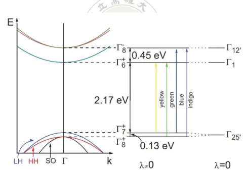
1.1.2 Band structure and Optical transitions
In Cu2O the valence band maximum and the conduction band minimum lies at the center
of the Brillouin zone, as shown in Fig 1.2. The highest valence band is split in to upper Γ7+ band
and lower Γ8+ band with energy split of SO= 133.8 meV due to the spin orbit coupling. Because
the lowest CB and the split valence bands have the same positive parity, so the transitions from VB (Γ7 + → Γ
6+, Γ8 + → Γ6+) to lowest conduction band are dipole forbidden; whereas transition to
next CB (Γ7 + → Γ8−, Γ8 + → Γ8− ) are dipole allowed [10].
The band to band direct forbidden transition Γ7 + → Γ6+ has energy of 2.173 eV which is limit of the yellow exciton series and transition from Γ8 + → Γ6+ has energy of 2.304 eV as limit
of green exciton series, the direct allowed optical transition Γ7 + → Γ
8− has energy of 2.624 eV as
limit of blue exciton series, transition from Γ8 + → Γ8− has energy of 2.755 eV as limit of indigo exciton series at 4.2K [5] .
Figure 1.2. The band structure of Cu2O near the center of Brillouin zone and transition of the
four excitonic series with spin orbit interaction (λ≠0) and when spin orbit interaction is not accounted for (λ=0) [11].
4
At the top of valence band Γ7 + has light effective hole mass that is nearly half of the electron
effective mass. Both light hole and electron effective masses are isotropic and heavy holes and spin orbit hole masses are anisotropic. DFT Calculation and experimentally determined effective electron and hole masses expressed in units free electron mass (m0) along Γ-X (100), Γ-M (110),
Γ-R (100) directions are given in Table 1.1 [11].
Table 1.1. Electron and hole effective masses from DFT calculation and experiments [11].
Mass Band Calculated Experiment
𝚪 − 𝐗 𝚪 − 𝐌 𝚪 − 𝐑 Average 𝐦𝒆 ∗ Γ6 + 0.92 0.92 0.92 0.92 0.99 (0.93+) 𝐦𝒍𝒉 ∗ Γ7 + 0.36 0.36 0.36 0.36 0.58 (0.56+) 𝐦𝒉𝒉 ∗ Γ8 + 2.83 0.91 0.72 1.49 𝐦𝒔𝒐𝒉 ∗ Γ8 + 0.21 0.25 0.27 0.24 + Polaron corrected
1.1.3 Electrical properties and defect states
In p-type oxide semiconductors, oxygen 2p orbitals are strongly localized so that valence band edge has a small dispersion causing the holes to have heavy effective mass that results in low hole mobility. By introducing covalency by hybridization of d orbitals in metal cation and oxygen 2p orbitals the localized band edge is changed to extended structure, consequently the acceptor level is also lowered. The thermally activated holes can migrate within the host lattice due to the extended nature of the valence band edge independent of the doping level. Hence, it is important to find oxide that has a closed shell d orbital (to avoid coloration due d-d transition) that has the same or closer energy level so that it can form bonds oxygen 2p orbitals with considerable covalency that reduce localization and lead to more dispersive VBM. Cu+ and Ag + ions satisfy this electronic structure with closed shell d10s0 configuration [2].
The electronic structure of copper ion ends with 3d104s0 level. In Cu2O, 3d level
5
in Fig 1.3. Cu 3d level is closer to O 2p orbital thus, the valence band maxima is dominated of 3d orbital, resulting in dispersed VBM and light effective hole mass [3]. While this character leads to higher hole mobility, it does not lead to origin of holes in Cu2O. The Cu2O has stable high
concentration of holes and the holes originate from the point defects within the crystal [13].
Figure 1.3. Chemical bond between Cu cation with closed shell configuration and oxide ion [2]. Origin of holes in Cu2O has been mainly attributed to two types of Cu vacancy (VCu) and
split Cu vacancy (VCusplit) which moves from its initial position towards to Cu vacancy,
producing stable defect state by coordinating with 4 neighboring oxygen atoms. VCu produces
shallow acceptor like state that can readily release holes about 0.28 eV over VBM with smallest formation energies (around 1 eV) both under Cu rich/ O poor and Cu poor/ O rich conditions, as shown in Fig 1.4. Both Cu vacancies are different regarding to the arrangement of atoms around it, but the formation energies are very close in value [14].
6
Figure 1.4. Defect formation energies in Cu2O as a function of the Fermi energy EF under a) Cu
rich-oxygen poor, b) Cu poor-oxygen rich conditions. (+), (–), (2–) indicate the charge state [13]. Another potential producer of holes is oxygen interstitials (Oi), there are two types of
oxygen interstitials at tetrahedral and octahedral sites with almost no distinct difference in their formation energies. Oi have slightly higher formation energy than VCu in both Cu rich/ O poor
and Cu poor/ O rich conditions and so the majority of holes are contributed from VCu. Moreover,
the potential hole killers are O vacancy which has slightly higher formation energy than VCu but
only stable in charge neutral state and Cu interstitials (Cui) have very high formation energy
which makes it very unlikely appear. These characteristics make Cu2O native p-type
semiconductor and very attractive candidate as p type semiconductor applications [13].
1.1.4 Oxidation of copper oxides
Copper oxide with p-type characteristics exist in three types of phase: Cupric oxide (CuO), Cuprous oxide (Cu2O) and Paramelaconite Cu4O3. In ambient conditions most stable phase is
CuO and although the Cu2O phase is unstable and oxidized to CuO. The oxidation process is
very slow that Cu2O is considered stable phase at ambient. Cu4O3 phase unstable at ambient
atmosphere. Pressure-Temperature phase diagram of copper oxides are theoretically calculated and experimentally determined by different research groups at moderate to high temperatures and is in good agreement with each other [11, 13]. As shown in Figure 1.5, the Cu2O is only
7
Li et al. studied the oxidation and reduction of copper oxide thin films and offer some insight into equilibrium phase relationship and oxygen in and out diffusion on the phase transformation of copper oxides. They studied the reduction and oxidation of CuO, Cu2O and
sputtered Cu4O3 film by annealing in vacuum (P = 210-7 Torr) and oxygen ambient in quartz
tube furnace.
Their results indicate that the phase transformation from CuO to Cu2O starts at 350oC and
the transformation is completed at 750oC in vacuum. At 350oC for 12 hours of annealing the two phases of the oxides still coexisted, and after annealing temperature was raised to 610oC the CuO was completely transformed to Cu2O phase. The transformation of CuO thin film on Si substrate
to Cu2O was completed at 750oC for 30 min in vacuum. Cu2O was then oxidized to CuO phase
completely in 15 minutes by annealing in oxygen ambient at 350oC. The rate of oxidation is
much faster that reduction in copper oxides. On the other hand, phase transformation from Cu4O3
phase to CuO phase starts at 250oC in oxygen ambient and Cu2O at 340oC in annealing in
vacuum both lower temperature than the phase transformation from Cu2O to CuO phase and vice
versa. The study suggests the grain boundary, composition and impurity affects the transformation temperature of the CuO to Cu2O [15].
Figure 1.5. Oxygen pressure vs temperature diagram shows stability of copper and its oxide phases [15].
8
1.2. Review of recent literature on Cu2O thin film fabrication.
As stated before there are many different techniques to fabricate Cu2O thin films and
brief summary of the recent research on the Cu2O film is described in this section.
Thermal oxidation is one of the conventional methods for preparing high-quality oxides because of its simplicity and low cost. The pure Cu2O phases are obtained around 200-250oC and
above 300oC CuO phase can be obtained [1]. In 2019, Cheon et al. reported thermal oxidation of epitaxial Cu2O film from single crystal Cu thin film by rapid thermal oxidation method. They
successfully fabricated Cu2O film with hole mobility of 41cm2/Vs in temperature range of
800-900oC under argon gas with oxygen partial pressure of 210-3 Torr [5].
Vacuum based methods show the best results in fabricating high quality epitaxial Cu2O
thin film with high hole mobility. The highest reported hole mobility of 256cm2/Vs in Cu
2O film
was fabricated with RF sputtering by Li et al. by introducing low temperature Cu2O buffer layer.
Sohn et al. has reported the Cu2O film grown by RF sputtering can be annealed in vacuum in
temperature of 700oC without phase transition into Cu. The hall mobility of the film was
increased from 0.02 cm2/Vs to 47.5 cm2/Vs after annealing, demonstrating that Cu2O film can be
further annealed in vacuum atmosphere to improve the crystallinity of the film and reduce the strain and disorder within the film for more improved optical and electrical properties [16]. Han
et al. also reported similar result in fabricating p-channel thin film transistor with Cu2O thin film
grown by sputtering and post deposition annealing in vacuum [6].
Another way to produce high quality epitaxial Cu2O film is trough pulsed laser
deposition method (PLD). PLD utilizes high energy laser pulse to grow epitaxial film under high vacuum and high temperature. High quality Cu2O film with Hall mobility in range of 30-107
cm2/Vs were fabricated in temperature range of 500-700oC [1]. Moreover, Farhad et al. have fabricated Cu2O thin film tunable n- and p-type properties by varying the oxygen partial pressure
[17].
On the other hand, solution-based methods are attractive for large scale production of film in electronic applications. Solution based methods are wide in range like chemical bath
9
deposition, electrochemical deposition, hydrothermal synthesis, sol-gel, spray pyrolysis etc. Here some of the notable results using solution-based fabrication of Cu2O thin films are described
briefly.
One of the solution-based methods is spray pyrolysis. Spray pyrolysis methods utilizes a simple downward spraying of precursor solution containing Cu ions onto a heated substrate. The method is easy and quick and well suited for large scale fabrications. Nitta et al. reported Cu2O
film with varying growth orientation from [111] to [110] using copper sulfate and NH3 and
NaOH as reaction solution to obtain film with band gap in range of 2.05 - 2.20 eV at 70oC. the growth orientation was influenced by the ratio of NH3 and NaOH, with higher NH3 concentration
leading to growth preference in [110] direction [18]. Also, Rivera et al. reported obtaining Cu2O
film by spray pyrolysis at temperature range of 330-340oC. At below this temperature range, the film had Cu phase and above the 340oC the film had CuO phase. Thus the processing window for obtaining Cu2O is very narrow at ambient atmosphere [19].
Chemical bath deposition is a simple coating method by dipping a substrate into a bath of a precursor solution. But the method is not very suitable for growing film on large substrates and requires relatively large amount of precursor solution and the solution is not reused after the deposition process. But this problem has been addressed by using modified technique to reduce the amount of precursor solution used. One of the examples is reported by Altindemir et al. They fabricated Cu2O film with high hole mobility in range of 23-174 cm2/Vs using four different
copper salts as precursor at 60oC using successive ionic layer adsorption method, a modified
chemical bath deposition method [9].
Another of well-known solution-based method is electrochemical deposition technique. This method deposits metal oxide film from simple metal ion complex solution. One advantage of this method is possibility of varying the growth preference of Cu2O thin film by modifying the
solution pH and applied voltage during the deposition process. In 2015, Wu et al. reported fabrication of Cu2O film using electrochemical deposition method on ITO substrate with varying
pH of solution to control the growth orientation of the Cu2O film from [100] to [110] to [111]
10
film can be effectively controlled by the pH of the solution in this method [7]. However, since the electrochemical deposition method requires the use of conductive substrate the accurate determination electrical characterization of the resulting film is complicated [20].
Next, Sol-gel method is one of wet chemical techniques widely used in fabrication of metal oxide materials. The method typically utilizes metal alkoxide precursor molecules to produce solution “sol” and gradually forms the “gel” diphasic system containing both liquid and solid phase. The process runs through several stages starting with colloidal solution preparation by hydrolysis condensation and then after gelation followed by drying processes. This method can be used for producing a wide range of micro and nanostructures like particles, tubes, hollow spheres, cages etc. Also, precursors can be deposited onto various substrates to produce thin films using dip coating or spin coating method [21]. Some of the results of sol gel derived Cu2O
thin films are described below.
Ray et al. prepared Cu2O thin film (2.10 eV) using dip coating technique and post
annealing at 360-500oC. The film was in Cu2O phase at 360oC and 400oC, then at 500oC the film
fully converted to CuO phase [22]. Armelao et al. synthesized Cu2O film by also dip coating
technique and post annealing at 100-900oC in various conditions with of air, nitrogen and forming gas (95% N2 + 5% H2). The Cu2O film was successfully fabricated at 900oC for 5 hours
under inert atmosphere and 500oC for 1 hour under reducing conditions [8].
Nagai et al. have demonstrated the fabrication of Cu2O film by different approach, using
molecular precursor Cu2+ complex with EDTA and spin coating on glass substrate, followed by a post treatment at 450oC in Ar gas, which resulted in a transparent Cu2O film with optical band
gap of 2.3eV and hole mobility of 4.8 cm2/Vs [23].
Kim et al. successfully fabricated p-channel thin film transistor with sol gel processed Cu2O in two step annealing under nitrogen and oxygen atmosphere for the first time. The
as-annealed film under N2 had mainly Cu phase indicating need for additional annealing under O2.
The oxygen partial pressure (PO2) were 0.04, 0.2, 0.9 Torr, and Cu2O film was obtained at PO2 of
0.04 and 0.2 Torr and at 0.9 Torr, CuO phase has appeared. The resulting TFT have field effect mobility of 0.16 cm2/Vs and Cu2O film had hall mobility of 18.9 cm2/Vs [24].
11
Jang et al. fabricated TFT with sol gel processed Cu2O and CuO thin film with filed
effect mobility of 2.010-3 cm2/Vs and 1.010-2 cm2/Vs respectively. The Cu2O film was
obtained at 200oC for 4 hours in air. Annealing time played an important role in obtaining Cu2O,
when annealed for 1 hour, film was in metallic Cu phase and when annealed for 12 hours, the film consisted of Cu2O and Cu phases [25].
Yu et al. reported solution processed TFT with Cu2O film using one step vacuum
annealing. The sol gel deposited films were post treated at 400 - 700oC for 2 hours under base pressure of 210-6 Torr. At 400oC the film consisted of CuO phase and as the temperature increased the CuO phase was converted to Cu2O and at 600 and 700oC, the film was fully
converted to Cu2O. With increasing temperature (400-600oC) the field effect mobility was
increased from 0.05 to 0.29 cm2/Vs, however at 700oC the mobility dropped to 10-2 cm2/Vs [26].
Similar results of applying vacuum annealing to improve electrical performance of Cu2O film
were also reported by Han et al. after deposition of Cu2O thin film by reactive sputtering. The
deposited Cu2O did not go through phase conversion after vacuum annealing at temperature up
to 700oC for 10 min under base pressure of ~ 7.110-4 Torr. In contrast to results of Yu et al, after annealing at 700oC the electrical properties of the film did not deteriorate but improved due to reduction of disorder in the film at high temperature annealing, revealed by analyzing the Urbach energy of the film [6].
Sohn et al. fabricated Cu2O thin film transistor film by vacuum annealing (210-6 Torr)
CuO film deposited by RF magnetron sputtering on SiO2/Si substrate at 350 and 500oC for 7
min. At 350oC the film consisted of both CuO and Cu2O phase and at 500oC the film only
consisted of Cu2O. Cu2O film had hall mobility of 47.5 cm2/Vs and field effect mobility of 0.07
cm2/Vs [16].
In 2015, temperature dependent spectral studies were performed by Yu et al. They were able to obtain pure Cu2O thin film through sol gel method and rapid thermal annealing under N2
12
1.3. Research purpose/motivation
When fabricating thin films by sol gel method, characteristics of the film can be regulated by many factors involved in the process. The typical process of growing oxide semiconductor thin film involves precursor solution preparation, coating, and annealing. After the deposition, for formation of uniform and improving the structural quality of films high temperature post annealing step. As described previously, in oxygen rich atmosphere the annealing temperature over 300oC results in CuO phase change, while in oxygen poor atmosphere like in vacuum, under nitrogen and argon gas or reducing atmosphere then moderate to higher temperatures can be used to fabricate Cu2O. Cu2O is sensitive to phase conversion depending on the annealing
environment, and difficult phase to obtain as opposed to CuO. In reviewing of recent research works on sol-gel growth of pure Cu2O, processing window for obtaining pure Cu2O can be very
narrow and could require precise control of the temperature and oxygen pressure. Therefore, unlike complicated route adopted by the other research groups, such as chemically modified Cu-O structures before annealing or precise control of post-annealing temperature and duration at a relatively high vacuum above 10-4 Torr, we attempt to grow Cu
2O films by post-annealing
preformed CuO or non-crystallized Cu-O structures under an optimum oxygen partial pressure over the temperature range from 600 oC to 900oC. The high temperature adopted here is expected
to obtain a high crystalline quality Cu2O. In other words, the purpose of this work is to introduce
a simple approach to fabricate Cu2O thin film using solution method, specifically sol-gel
technique with one step annealing in vacuum atmosphere in broad range of temperature. We aimed to study the following in this work:
- Effects of the post annealing temperature, atmosphere, and duration on obtaining pure Cu2O phase.
- Determine the optimal conditions to obtain Cu2O thin film.
- Effects of the post annealing condition in the structural properties of the film, investigated by spectroscopic methods
13
2. EXPERIMENTAL SECTION 2.1. Cu2O thin film growth
In this work, the precursor solution was prepared using copper nitrate trihydrate salt (Cu (NO3)2 · 3H2O) as a copper source, monoethanolamine (MEA) as a stabilizer and isopropanol
(IPA) or water as a solvent. The precursor solution was prepared with 0.6 moles of copper ion: MEA with a ratio of 1:0.5. After the addition of the solvent, the solution was stirred at 55oC for 1 hour with magnetic stirring at 450 rpm. Then, the solution was filtered through Whatman 52 filter paper and aged at room temperature for up to 7 days.
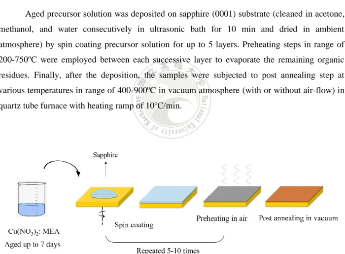
Aged precursor solution was deposited on sapphire (0001) substrate (cleaned in acetone, methanol, and water consecutively in ultrasonic bath for 10 min and dried in ambient atmosphere) by spin coating precursor solution for up to 5 layers. Preheating steps in range of 200-750oC were employed between each successive layer to evaporate the remaining organic residues. Finally, after the deposition, the samples were subjected to post annealing step at various temperatures in range of 400-900oC in vacuum atmosphere (with or without air-flow) in quartz tube furnace with heating ramp of 10oC/min.
14
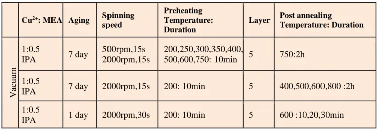
Detailed growth parameters of the samples are summarized in Table 2.1. and Table 2.2. Table 2.1. Growth parameter of Cu2O thin film samples annealed in vacuum
Cu2+: MEA Aging Spinning
speed
Preheating Temperature: Duration
Layer Post annealing
Temperature: Duration V ac uum 1:0.5 IPA 7 day 500rpm,15s 2000rpm,15s 200,250,300,350,400, 500,600,750: 10min 5 750:2h 1:0.5
IPA 7 day 2000rpm,15s 200: 10min 5 400,500,600,800 :2h
1:0.5
IPA 1 day 2000rpm,30s 200: 10min 5 600 :10,20,30min
Table 2.2. Growth parameter of Cu2O thin film samples annealed under air flow
Cu2+: MEA Aging Spinning speed Preheating Layer Post annealing
A
ir fl
ow
1:0.5 Water
1 day 1500rpm,15s 300: 10min 5 400,500,600,750 :30 min
PO2= (1.90.2)10-3 Torr
1:0.5 Water
1 day 1500rpm,15s 300: 10min 5 600: 30min, 2hours
PO2= (4.80.1)10-3 Torr
1:0.5 Water
3 day 2500rpm, 60s 300: 10min 5 600: 2, 4, 6, 8 hours
PO2= (3.20.4)10-3 Torr 1:0.5 Water 4-5 day 2500rpm, 60s 300: 10min 5 600,700,800,900: 30 min PO2= (5.60.1)10-3 Torr 1:0.5 Water
5 day 2500rpm, 60s 300: 10min 5 700: 2, 4 hours
PO2= (5.70.2)10-3 Torr
1:0.5 Water
5 day 2500rpm, 60s 200,300,700: 10min 5 700: 2 hours
15
2.2. X-ray diffraction analysis
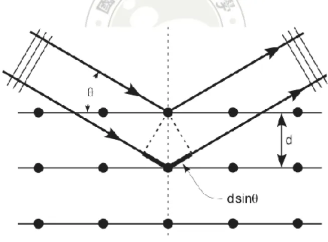
X-ray diffraction technique is a non-destructive technique that is used to identify and analyze the structure of minerals, as well as other crystalline materials. When X-ray is diffracted by the ordered atoms in the lattice planes, diffracted rays form a constructive interference. As illustrated in Figure 2.2. X-ray beam with same wavelength and phase are scattered by the atoms with interplanar spacing d the second beam travels extra length of 2dsinθ. We can measure the distances between the planes of the atoms that constitute the sample by applying the Bragg's Law.
nλ = 2dhklsinθ
Where the integer n is the order of the diffracted beam, λ is the wavelength of the incident X-ray beam, d is the distance between adjacent planes of atoms (the d-spacings), and θ is the angle of incidence of the X-ray beam. The diffracted peaks at these incident angles determine the each crystal planes present in the sample [28].
Figure 2.2. Schematic illustration of Braggs law.
The crystal structure of the Cu2O sample was identified using XRD at room temperature.
The XRD analysis was done with a diffractometer operating at 40kV and 40mA with Cu Kα (=1.54184Å) radiation. Sample were analyzed with 3 degrees/min with spin and diffraction angle range of 20-80 degrees. The results were analyzed with MDI Jade 6 with JCPDS file database. The results were analyzed with MDI Jade 6 with JCPDS file database and crystal phases are assigned with CuO (PDF 80-0076 ), Cu2O (PDF 78-2076 ) and Cu (PDF 85-1326) cards.
16
2.3. Raman spectroscopy
When light is incident on sample when the scattered light has no loss of energy or no frequency change then this type of scattering is Rayleigh scattering which is elastic scatting process. In the contrary, Raman scattering is inelastic scattering process, where the frequency and the wavenumber of the incident beam is changed during interaction with the phonons in the sample. When incident photon transfers its energy to the crystal lattice causing lattice vibration in the sample and the photon energy is reduced with higher frequency of phonon, the more energy is transferred according to the momentum and energy conversion and scattered in different direction. This phonon creation process is called Stokes process and reversibly if there is energy of phonon transferred to the incident photon resulting in photon with higher frequency then the process is called anti-Stokes process [29].
17
Not all phonon modes in solids are Raman active and its due to the selection rule. Selection rule of Raman scattering is determined by polarizability change during vibration. Raman analysis can be effective tool for phase analysis as materials can be characterized by their unique vibrational modes [29].
For the purpose of confirming the copper oxide phase, Micro-Raman spectra were recorded with at 300 K. For sample excitation, a diode laser with 532 nm wavelength was used. Characteristic phonon modes related to Cu2O were identified based on Table 2.3.
Table 2.3. Symmetry and characteristic Raman shift observed experiment and theoretical study of Cu2O [26, 27]. Label Symmetry Classification Mulliken Symbol Degeneracy Experiment (cm-1) DFT (cm-1) Nominal Activity A − T2u 3 85-100 71 Silent B − Eu 2 107-110 84 Silent C − T 1u(TO) 2 140-152 147 Infrared − T1u(LO) 1 150-160 148 Infrared D − A2u 1 308-350 338 Silent E + T2g 3 515 499 Raman F − T1u(TO) 2 608-635 608 Infrared − T1u(LO) 1 650-665 630 Infrared
18
2.4 Photoluminescence
Photoluminescence is nondestructive spectroscopic technique applied for material characterization. Photoluminescence (PL) is a process absorption high frequency (hν > Eg) light
by semiconductor exciting electrons and subsequent emission of photons as relaxation of electrons to ground state. Many localized defect states in crystal lattice can serve as radiative recombination centers. Consequently these imperfections can be detected by PL spectroscopy and resulting PL spectra can be used to identify the specific type of semiconductor defect [32].
The samples were mounted on closed cycle cryostat (CTI-Cryogenics) with copper plate. The temperature of the sample chamber is monitored and controlled by heater in range of 25K to 300K. The excitation source was Nd:YAG laser with 355 nm wavelength (photon energy of 3.49 eV). The light beam was focused on a sample surface in horizontal direction by combination of reflective mirrors. The PL signal was detected by air cooled charge coupled device camera after dispersion by monochromator /Horiba iHR320.
19
3. RESULTS AND DISCUSSION
3.1. Effects of annealing temperature and duration on post annealing in vacuum
First, series of XRD measurements were done to determine the state of the film before the post annealing step to realize the influence of structure of intermediate state on the formation of the Cu2O thin film. For this purpose, different preheating temperatures in the range of 200 to
750oC were used to preheat the samples to evaporate the organic residues between each successive layer. The results are shown in Figure 3.1. The sample preheated at 200oC does not show any diffraction peaks and is in amorphous state. Therefore, preheating in 200oC for 10 min does not provide enough thermal energy to drive formation any crystalline phase in air. However, starting from the samples preheated at 250oC further to 750oC, the presence of CuO characteristic peaks starts to appear therefore the film is starting to transform in to crystalline state and the intensity of the CuO diffraction peaks become more intense as the temperature increases.
20
Subsequently the preheated samples were all subjected to post annealing step in vacuum at 750oC, temperature was chosen according to the phase diagram of the copper oxide in Figure
1.5. The intensity of the XRD results are normalized to Cu (200) peaks, to further investigate the influence of the state of the films during preheating step on the final product, the XRD measurement was done after the post annealing step. As seen from Figure 3.2 the resulting films all transformed to the Cu2O and metallic Cu phase after annealing in a vacuum at 750oC for two
hours. But film is mostly dominated by the Cu phase over Cu2O.
Figure 3.2. XRD patterns of film post-annealed at 750oC for 2 hours in vacuum.
Since the state of the film before the post annealing step is CuO phase, then the post annealing in vacuum atmosphere should promote the reduction of the CuO due to lack of oxygen in vacuum atmosphere as indicated in the equation below.
21
Furthermore, with higher preheating temperature the presence Cu2O phase is more
intense as observed from the XRD patterns normalized to Cu (200) peak intensity. This may indicate the formation of Cu2O phase from CuO phase through oxide reduction in oxygen poor
atmosphere is more efficient than formation of Cu2O phase from non-crystalline Cu-O chains.
This is not surprising since under the annealing ambient, the oxygen reduction process 2Cu2O
4Cu + O2 is efficient and to obtain the Cu2O phase, oxygens supplied by the pre-existed CuO is
necessary. In short conclusion, at post annealing temperature of 750oC, there is strong presence of Cu phase and we cannot obtain the pure Cu2O films because of the efficient oxygen-reduction
process.
Therefore, we studied the post-annealing temperature effect on the oxygen-reduction process. 400oC to 800oC are used for the post annealing step in vacuum to study the effects of
temperature. The samples are preheated at 200oC. XRD results of the samples subjected to post
annealing at 400oC, 500oC, 600oC, and 800oC in vacuum atmosphere with pressure of (2.40.3)10-2 Torr for 2 hours are shown in Figure 3.3. It clear that all the samples almost fully composed of Cu phase. Even after annealing at lower temperature of 400oC the film is still fully reduced to Cu phase, despite the phase diagram shown in Figure1.5 indicates the reduction to Cu phase happens at higher temperature with oxygen partial pressure of ~10-3 Torr. These results show that the post-annealing temperature is not a crucial factor that can control the oxygen-reduction process.
22
Figure 3.3. XRD patterns of film annealed at 400oC - 800oC two hours under vacuum (P= (2.40.3)10-2 Torr
Since the post annealing at lower temperature in vacuum still resulted in Cu film, the influence of the annealing duration was studied at temperature of 600oC. The target of this investigation is to examine whether the oxygen-reduction process can be controlled by annealing-duration or not. Figure 3.4 shows the XRD patterns of the films deposited at preheating temperature of 200oC and 600oC and post annealed at 600oC in vacuum atmosphere with base pressure of (2.70.5)10-2 Torr for 10, 20 and 30 minutes.
23
Figure 3.4. XRD patterns of film annealed at 600oC for 10–30 minutes under vacuum (2.70.5)10-2 Torr
After annealing at 600oC for 10 minutes, almost all of CuO phase has already
disappeared and there is small peak of Cu2O (111) phase. Cu phase starts to emerge as seen with
presence of Cu (111) and (200) peaks. As the annealing duration is increased to 20 minutes the Cu2O (111) peak is still present and traces of CuO phase is not seen. Furthermore, the intensity
of the Cu phase is increased and additional Cu (220) peak has been appeared. After 30 minutes the Cu2O phase has disappeared and the films are fully reduced Cu phase. This result shows that
even after annealing for short durations the results are same with Cu phase. Thus, we cannot obtain Cu2O film under vacuum annealing without supplying air or oxygen into the annealing
tube.
The results from this section all show that annealing CuO film in vacuum atmosphere results in Cu phase due to lack of oxygen. This probably result of the oxygen in CuO film is pumped out of the annealing tube and CuO reduced to Cu phase during annealing. These results
24
are quite contradictory to previously reported result by Yu et al mentioned in the literature review section where Cu2O film was successively obtained using sol-gel technique with post
annealing at 500-700oC in vacuum atmosphere with base pressure in range of 2 x 10⁻⁶ for 2 hours. But this difference in results is probably due to the different annealing conditions where the vacuum base pressure is significantly higher than discussed here. Also the crystalline form and thickness of the film before post annealing are not discussed by Yu et al , which could affect the formation of the Cu2O phase [26].
After several attempts, it was found that to obtain pure Cu2O phase in vacuum
atmosphere may require certain pre-conditions, such as crystalline structures before the post-annealing, thickness of films and so on. Therefore, to directly get the pure Cu2O films without
attempting abundant growth-parameters, we tried to control the oxygen-reduction process by supplying airflow and controlling the oxygen partial pressure by using a diaphragm-pump in the post-annealing process.
25
3.2. Effects of post annealing temperature and oxygen partial pressure on Cu2O film
Since the results from post annealing the film in vacuum resulted with Cu phase rather than Cu2O phase, this section describes the results of post annealing step performed with air flow to
supply the oxygen needed in oxygen poor vacuum environment to obtain Cu2O film.
Figure 3.5 shows the crystalline phase of the film deposited at preheating temperature of 300oC and post annealed at 400oC to 750oC with air flow for 30 minutes at oxygen partial pressure PO2 of (1.90.2)10-3 Torr. The intensities are normalized at Cu (200) peak intensity.
After introducing oxygen by flowing air during the post annealing step, the results show that the films annealed at 400, 500, 600 and 750oC now contain both Cu
2O and Cu phase. The film
annealed at the 600oC shows most intense Cu
2O (111) peak compared to other samples in this
result. But the films still have Cu phase present, so the low oxygen partial pressure during the annealing step is insufficient to obtain pure Cu2O phase.
Figure 3.5. XRD patterns of film annealed at 400oC - 750oC for 30 minutes with air flow (PO2 =
26
Therefore, the preformed films with CuO phase deposited at preheating temperature of 300oC were subjected to post annealing step at 600oC, which is chosen based on the intensity of the
Cu2O phase from this result. The effect of oxygen partial pressure and longer duration at post
annealing step were studied further.
Figure 3.6. XRD patterns of film annealed at 600oC for 30 minutes with air flow
At higher degree of oxygen partial pressure PO2 = (4.81.1)10-3Torr, the film consisted mainly of CuO phase and very small Cu2O phase when annealed for 30 minutes. Furthermore, when the film annealed for longer duration of 2 hours, the intensity of the Cu2O phase became
more pronounced. These results indicate that when annealing at 600oC, at oxygen partial pressure around (4.81.1)10-3 Torr and with longer annealing durations, we might be able to obtain pure Cu2O film.
Subsequently, to study the effect of the annealing duration at the post annealing step at 600oC with oxygen partial pressure of (3.20.4)10-3 Torr, films deposited at preheating
27
temperature of 300oC were annealed for 2, 4, 6 and 8 hours. The results are shown in Figure 3.7. As the annealing duration is increased the more CuO phase is transformed into Cu2O phase.
After annealing for 2 and 4 hours the films both show similar results with both Cu2O and CuO
phase. But the Cu2O peak intensity is clearly stronger than that of CuO phase. Furthermore after
6 hours the CuO phase is almost fully transformed into Cu2O phase. Finally, after 8 hours of
annealing, pure Cu2O film is obtained with no phase transformation into Cu phase.
Figure 3.7. XRD patterns of film annealed at 600oC for various duration at oxygen partial pressure of (3.20.4)10-3 Torr
Since we can obtain pure Cu2O film by annealing CuO film at 600oC with oxygen partial
pressure of (3.20.4)10-3 Torr. Afterwards, we have studied the effect of the higher annealing temperature on the reduction of CuO film at slightly higher degrees of oxygen partial pressure.
28
The films deposited at preheating temperature of 300oC were subjected to post annealing at 700, 800 and 900oC with oxygen partial pressure of (5.60.1)10-3 Torr for 30 minutes. The XRD results are shown in Figure 3.8. As the post annealing temperature is raised to 700, 800 and 900oC the CuO film is fully converted to Cu2O phase just after 30 minutes. Even after annealing
at 900oC there is no Cu phase present. Results show that although at 600oC we could be able to obtain Cu2O phase, but the annealing duration is significantly higher compared to higher
temperature annealing. So, the 600oC does not provide enough thermal energy to fully convert CuO phase into Cu2O phase in short amount of time. Therefore, if the higher temperature up to
900oC is used for post annealing step then we can get Cu2O film with much shorter annealing
time.
Figure 3.8. XRD patterns of films annealed at 600 - 900oC for 30 min at oxygen partial pressure
29
3.3. Effect of post annealing duration Cu2O film at various temperatures.
The effect of post annealing duration was studied at 700oC and oxygen partial pressure of (5.70.2)10-3 Torr. The CuO films preheated at 300oC were subjected to post annealing for 30 minutes, 2 hours and 4 hours and results of the XRD is shown in Figure 3.9.
Figure 3.9. XRD patterns of films annealed at 700oC for 0.5 hr, 2hrs and 4hrs with oxygen partial pressure of (5.70.2) 10-3 Torr
The results show that in all samples CuO phase is fully transformed to Cu2O phase.
Additionally, after annealing for 4 hours there is no further reduction into Cu phase. Compared with the results shown in Fig 3.6, within the oxygen partial pressure PO2 ~ 510-3 Torr, we found
30
Furthermore, to determine if the crystalline phase of the film before post annealing step affects the phase of the film after annealing, films preheated at three different temperatures were analyzed. Sample preheated at 200oC, 300oC, and 700oC have subjected to post annealing at 700oC for 2 hours and normalized XRD pattern at sapphire (0001) peak is shown in Figure 3. 10. The results show that the all three samples are composed of Cu2O phase. As shown in the results
of XRD analysis after the preheating step in Fig 3.1, at 200oC the sample is in amorphous state and at 300oC and 700oC, samples are composed of CuO phase. These results indicate regardless of the initial crystalline state of the film before the annealing process, pure Cu2O film can be
obtained if the temperature and oxygen partial pressure are well-controlled.
Figure 3.10. Normalized XRD patterns of films preheated at 200oC, 300oC and 700oC annealed at 700oC for 2hrs with oxygen partial pressure of (5.70.2)10-3 Torr
31
3.4. Post annealing temperature and duration on Raman scattering in Cu2O film.
In order to investigate the crystalline structures of the samples, we performed the Raman spectroscopic studies on the Cu2O films. Cu2O unit cell contains 6 atoms, therefore there are 18
vibrational modes of which 15 optical phonon modes and 3 are acoustic modes. The symmetries of the vibrational modes at k=0 are:
A2u ⊕ E2u ⊕ 3T1u ⊕ T2u ⊕ T2g
Phonons with A, E and T are one, two and threefold degenerate. Three acoustic modes possess the T1u symmetry and two remaining modes of T1u belong to the infrared active optical
lattice vibrations. Phonons with A2u, E2u, T2u are silent modes. Theoretical group theory analysis
suggests perfect crystal of Cu2O should exhibit only one Raman active mode belonging to the
threefold degenerate T2g mode. The other modes stem from breaking of symmetry from the
defects within the crystal [25, 26].
Figure 3.11. Schematic illustration of zone-center phonon modes in Cu2O [14].
All the vibrational modes described above appears in Raman spectra of the Cu2O samples
32
In Fig. 3.12, we showed the Raman spectra of films with pure Cu2O-phase,
post-annealing at 600, 700, 800 and 900oC. In the figure, there are two Raman curves (black and yellow), labelled by 700oC-0.5 hr, taken respectively from two samples grown under nearly identical condition. The two Raman spectra are nearly the same indicates that the crystal-structure of Cu2O films grown can be reproducible. As seen in Figure 3.12, the Cu2O films
post-annealing at 600 to 800oC exhibit Raman shifts at 91 cm-1, 106 cm-1, 145 cm-1, 219 cm-1, 309 cm
-1, 417 cm-1, 500 cm-1 and 628 cm-1. Similar Raman scattering modes were also found in the Cu 2O
samples grown by other methods, under the 532 nm-laser excitation at room-temperature [31]. Most intense signal of Cu2O samples is the second order overtone 2Eu (219 cm-1). Due to
the violation of intrinsic selection rule mechanism, other scattering from Raman forbidden first order modes T2u (91 cm-1), Eu (106 cm-1) and A2u (309 cm-1), second order 2Eu (219 cm-1) and
fourth order 4Eu (417 cm-1) silent mode have also been observed [24, 26]. T2u (91 cm-1)
represents rigid rotation of Cu4O tetrahedron around oxygen atoms which arise from transverse
vibration of Cu atoms. Phonon mode at Eu (106 cm-1) is twisting of Cu4O tetrahedron around the
c-axis. The Raman active mode correspond to the relative motion of two simple cubic O lattices [27]. Observed signal around 309 cm-1 may be attributed to the A
2u mode or sum of T2u and 2Eu
modes. Besides the silent modes, we can also observe the infrared mode T1u (TO, LO) at 145 cm -1 and 628 cm-1, as well as a weak Raman active signal around 500 cm-1.
There are two unidentified Raman modes appeared in our Cu2O samples, i.e., broad
Raman band centered around 576 cm-1 and a small Raman peak at 697 cm-1. The origins of these modes may be due to the surface-related defects, which will be discussed later.
33
Figure 3.12. Raman spectra of Cu2O film annealed at 600-900oC.
The Raman peaks positions and intensities are not very much distinct with different annealing temperature of 600oC, 700oC and 800oC except the film annealed at 900oC. In particular, the second order 2Eu (219 cm-1), fourth order 4Eu (417 cm-1), A2u (309 cm-1) silent
modes and the 145 cm-1-T1u infrared mode are missing in the sample annealed at 900oC.
Furthermore, the film annealed at 900oC have shown three sharp Raman peaks at 417 cm-1, 576 cm-1, and 750 cm-1, that are likely to have arisen from the sapphire (0001) substrate [33], owing to the thin thickness. This result is supported by the topography image of the Cu2O film annealed
at 700oC for 0.5 hour, 700oC for 1 hour and 900oC for 0.5 hour obtained with atomic force microscopy. The images are shown in Figure 3.13. The rough estimation of film thickness by analyzing the height histogram by assuming the lowest height is surface of substrate then the film thickness for the film annealed at 700oC for 0.5 hour and 1 hour are around 650nm, and
34
5.5nm, which shows that film annealed at 900oC is thinner that film annealed at 700oC and explain the appearance of Raman signals of sapphire substrate in spectra obtained from sample annealed at 900oC. This absence of other defect induced modes will be discussed later.
Figure 3.13. Atomic force microscopy images of Cu2O films annealed at 700oC for 0.5 hour,
700oC for 1 hour and 900oC for 0.5 hour.
Raman spectra of the Cu2O thin film sample annealed at 700oC for 0.5 – 4 hours are
shown in Figure 3.14. Also, there are two curves (red and green), correspond to the Raman spectra taken from two samples annealed at 0.5hr and 2hrs, grown under identical conditions. However, the two Raman curves (blue) are obtained from a Cu2O film at different positions. As
seen from the result, the samples annealed at 700oC for different durations, the signal of vibrational modes are almost identical except the film annealed for 1 hour. Besides the characteristic Raman modes mentioned above and reported in other literatures [14, 30, 31], two unidentified Raman modes are also observed in all of the samples. The film annealed for 1 hour shows almost the same Raman scattering signals as the sample annealed at 900oC but without the signals from the sapphire substrate, i.e., the silent modes and 145cm-1-T
1u infrared are almost
missing, compared with the samples annealed at 0.5, 2, 4 hours. Moreover, the film annealed at 700oC for 1 hour and 700oC for 0.5 hour have comparable thickness means this absence of
35
Figure 3.14. Raman spectra of Cu2O film annealed at 700oC for 0.5 – 4 hours.
In Ref. [31], Sander et al. studied the relations between the crystalline defects and the breaking of selection rules to observe silent modes in Cu2O crystals. They found that the infrared
and silent modes detected in Raman scattering of Cu2O are mainly induced by the presence of
copper split vacancy VCusplit, rather than the point defects such as oxygen and copper vacancies
or other oxygen and copper interstitial defects.
To confirm those facts, we measured the low-temperature photoluminescence spectra of relevant Cu2O samples, as shown in Fig 3.15. The absorption spectra of the typical Cu2O film
(black curve) annealing at 700 oC for 0.5 hour is also shown for reference. The absorption of photons starts from the onset of yellow band-gap (2.17 eV) and green band-gap (2.3 eV), described before at section 1.1.2. The absorption intensities are weak since these transitions are
36
dipole forbidden. The abrupt absorption edge nearly coincides at the dipole-allowed blue-gap. In the figure, the emission bands with peaks centered around 2.2 eV are observed for the Cu2O
samples annealing at 700 oC for 0.5 hr (red curve), 700 oC for 1 hr (green curve) and 800 oC for 0.5 hr (blue curve). In particular, the transitions related to copper vacancies VCu (1.35 eV), single
charged oxygen vacancies VO+ (1.53 eV) and double charged oxygen vacancies VO2+ (1.72 eV)
[34] are not detected. This indicates the observation of Raman-forbidden signal in our samples is not due to the point-defect mentioned above, consistent with those found by Sander et al. [31], i.e., the forbidden modes detected in Raman activities are mostly due to the existence of VCusplit.
The VCusplit is a split configuration of copper vacancy, where a Cu atom adjacent to vacancy
moves into a position between the corresponding two Cu lattice sites [14]. Therefore, a microscopic study may be necessary to clarify the absence of some silent and infrared mode in the Raman spectra of Cu2O films annealing at 700 oC for 1 hr and 900 oC for 0.5 hr.
Furthermore, to our best knowledge, the two unidentified Raman scattering modes located at 576 cm-1 and 697 cm-1 observed in all of the studied samples, were not reported so far. These Raman activities may due to surface-related defects, caused by dangling bond predictable in sol-gel derived samples, which rather possesses three-dimensional crystal-structures, in comparison with two-dimensionally grown Cu2O films. This may be evidenced by the broad
emission band spectrally centered at 2.2 eV, detected in our samples. The photoluminescence spectra of Cu2O recorded by other research groups usually shows some distinct peaks around 2.0
eV, originated from phonon-assisted recombination of 1S-yellow orthoexcitons [34]. However, the emission bands observed in our Cu2O films exhibit a very broad band with full-width at
half-maximum around 0.4~0.5 eV, spectrally located at the absorption edge of yellow-gap. Without the aid of breaking of crystal-symmetry such as surface-dangling bond, those broad emission bands are impossible. Therefore, further investigations are required to explore the origins in the future.
37
Figure 3.15. Photoluminescence spectra of Cu2O film annealed at 700oC (Green curve), 800oC
38
Results of this thesis is summarized schematically below in Figure 3.16.
39
4. CONCLUSION
• In first part of our experiment we have tried to fabricate Cu2O film from annealing CuO film
in vacuum atmosphere but were instead able to get Cu phase. When annealing in vacuum the temperature and duration had little impact in reduction of CuO to Cu phase. It was determined that without introducing oxygen obtaining Cu2O phase was not possible.
• However, by using post annealing under air flow we can obtain pure Cu2O phase by
controlling the oxygen partial pressure at higher temperature range (600-900oC) without
phase transformation to Cu. Additionally, this method is shown to produce a reproducible result and is more simple and stable way to grow Cu2O thin film.
• Raman and Photoluminescence measurements have confirmed the pure phase of Cu2O thin
films and defect induced vibrational modes in Raman spectra of Cu2O could be mainly due
to the split Cu vacancy. The Cu2O films in this work have shown two unidentified Raman
shifts at 576cm-1 and 697cm-1 which may be related to surface defects arisen from dangling bonds that are typical in sol gel derived films. However further microscopic studies needed to confirm these results.
40
5. REFERENCES
[1] H. A. Al-Jawhari, “A review of recent advances in transparent p-type Cu2O-based thin film transistors,” Materials Science in Semiconductor Processing, vol. 40. Elsevier, pp. 241–252, 2015.
[2] H. Kawazoe, H. Yanagi, K. Ueda, and H. Hosono, “Transparent p-type conducting oxides: design and fabrication of p-n heterojunctions,” MRS Bull., vol. 25, no. 8, pp. 28–36, 2000. [3] H. Kawazoe, M. Yasukawa, H. Hyodo, M. Kurita, H. Yanagi, and H. Hosono, “P-type
electrical conduction in transparent thin films of CuAlO2,” Nature, vol. 389, no. 6654, pp. 939–942, 1997.
[4] K. P. Ganesan, N. Anandhan, V. Dharuman, P. Sami, R. Pannerselvam, and T. Marimuthu, “Electrochemically modified crystal orientation, surface morphology and optical properties using CTAB on Cu2O thin films,” Results Phys., vol. 7, pp. 82–86, 2017.
[5] M. Cheon, B. Jung, S. J. Kim, J. I. Jang, and S. Y. Jeong, “High-quality epitaxial Cu2O films with (111)-terminated plateau grains obtained from single-crystal Cu (111) thin films by rapid thermal oxidation,” J. Alloys Compd., vol. 801, pp. 536–541, 2019.
[6] S. Han, K. M. Niang, G. Rughoobur, and A. J. Flewitt, “Effects of post-deposition vacuum annealing on film characteristics of p-type Cu2O and its impact on thin film transistor characteristics,” Appl. Phys. Lett., vol. 109, no. 17, p. 173502, 2016.
[7] W. Wu, K. Feng, B. Shan, and N. Zhang, “Orientation and Grain Shape control of Cu2O Film and the Related Properties,” Electrochim. Acta, vol. 176, pp. 59–64, 2015.
[8] L. Armelao, D. Barreca, M. Bertapelle, G. Bottaro, C. Sada, and E. Tondello, “A sol-gel approach to nanophasic copper oxide thin films,” in Thin Solid Films, 2003, vol. 442, no. 1–2, pp. 48–52.
[9] G. Altindemir and C. Gumus, “Cu2O thin films prepared by using four different copper salts at a low temperature: An investigation of their physical properties,” Mater. Sci.
Semicond. Process., vol. 107, no. August 2019, p. 104805, 2020.
[10] F. Biccari, “Defects and Doping in Cu2O,” 2009.
[11] B. K. Meyer et al., “Binary copper oxide semiconductors: From materials towards devices,” Phys. Status Solidi Basic Res., vol. 249, no. 8, pp. 1487–1509, 2012.
[12] W. Gao, M. Imran, M. K. Siddiqui, M. Naeem, and F. Jamil, “Molecular description of copper (I) oxide and copper (II) oxide,” Quim. Nova, vol. 41, no. 8, pp. 874–879, 2018. [13] H. Raebiger, S. Lany, and A. Zunger, “Origins of the p-type nature and cation deficiency
41
in Cu2 O and related materials,” Phys. Rev. B - Condens. Matter Mater. Phys., vol. 76, no. 4, pp. 1–5, 2007.
[14] D. Cakir, “Enhanced Raman signatures on copper based-material,” 2017.
[15] J. Li, G. Vizkelethy, P. Revesz, J. W. Mayer, and K. N. Tu, “Oxidation and reduction of copper oxide thin films,” J. Appl. Phys., vol. 69, no. 2, pp. 1020–1029, 1991.
[16] J. Sohn et al., “Effects of vacuum annealing on the optical and electrical properties of p-type copper-oxide thin-film transistors,” Semicond. Sci. Technol., vol. 28, no. 1, p. 015005, 2013.
[17] S. F. U. Farhad, D. Cherns, J. A. Smith, N. A. Fox, and D. J. Fermín, “Pulsed laser deposition of single phase n- and p-type Cu2O thin films with low resistivity,” Mater.
Des., vol. 193, 2020.
[18] R. Nitta, Y. Kubota, T. Kishi, T. Yano, and N. Matsushita, “One-step direct fabrication of phase-pure Cu2O films via the spin-spray technique using a mixed alkaline solution,”
Mater. Chem. Phys., vol. 243, p. 122442, 2020.
[19] D. Osorio-Rivera, G. Torres-Delgado, J. Márquez-Marín, R. Castanedo-Pérez, M. A. Aguilar-Frutis, and O. Zelaya-Ángel, “Cuprous oxide thin films obtained by spray-pyrolysis technique,” J. Mater. Sci. Mater. Electron., vol. 29, no. 1, pp. 851–857, 2018. [20] S. Han and A. J. Flewitt, “Control of grain orientation and its impact on carrier mobility in
reactively sputtered Cu2O thin films,” Thin Solid Films, vol. 704, p. 138000, 2020.
[21] C.-Q. Ye, “Sol-Gel Processes of Functional Powders and Films,” Chem. React. Inorg.
Chem., pp. 31–50, 2018.
[22] S. C. Ray, “Preparation of copper oxide thin film by the sol-gel-like dip technique and study of their structural and optical properties,” Sol. Energy Mater. Sol. Cells, vol. 68, no. 3–4, pp. 307–312, 2001.
[23] H. Nagai et al., “Chemical fabrication of p-type Cu 2O transparent thin film using molecular precursor method,” Mater. Chem. Phys., vol. 137, no. 1, pp. 252–257, 2012. [24] S. Y. Kim et al., “P-channel oxide thin film transistors using solution-processed copper
oxide,” ACS Appl. Mater. Interfaces, vol. 5, no. 7, pp. 2417–2421, 2013.
[25] J. Jang, S. Chung, H. Kang, and V. Subramanian, “P-type CuO and Cu2O transistors derived from a sol-gel copper (II) acetate monohydrate precursor,” Thin Solid Films, vol. 600, pp. 157–161, 2016.
[26] J. Yu, G. Liu, A. Liu, Y. Meng, B. Shin, and F. Shan, “Solution-processed p-type copper oxide thin-film transistors fabricated by using a one-step vacuum annealing technique,” J.
42
Mater. Chem. C, vol. 3, no. 37, pp. 9509–9513, 2015.
[27] W. L. Yu et al., “Diversity of electronic transitions and photoluminescence properties of p -type cuprous oxide films: A temperature-dependent spectral transmittance study,” J.
Appl. Phys., vol. 117, no. 4, p. 045701, 2015.
[28] C. Kittel and D. F. Holcomb, Introduction to Solid State Physics. 1967.
[29] E. Smith and G. Dent, Modern Raman Spectroscopy - A Practical Approach. 2005.
[30] K. Reimann and K. Syassen, “Raman scattering and photoluminescence in Cu2O under hydrostatic pressure,” Phys. Rev. B, vol. 39, no. 11, pp. 11113–11119, 1989.
[31] T. Sander et al., “Correlation of intrinsic point defects and the Raman modes of cuprous oxide,” Phys. Rev. B - Condens. Matter Mater. Phys., vol. 90, p. 045203, 2014.
[32] S. G. Bishop, “Characterization Of Semiconductors By Photoluminescence And Photoluminescence Excitation Spectroscopy,” in Optical Characterization Techniques for
Semiconductor Technology, 1981, vol. 0276, pp. 2–10.
[33] C. C. Kuo, W. R. Liu, W. F. Hsieh, C. H. Hsu, H. C. Hsu, and L. C. Chen, “Crystal symmetry breaking of wurtzite to orthorhombic in nonpolar a-ZnO epifilms,” Appl. Phys.
Lett., vol. 95, p. 011905, 2009.
[34] H. Solache-Carranco et al., “Photoluminescence and X-ray diffraction studies on Cu2O,”
![Figure 1.1. Crystal structure of Cu 2 O. a) Cu 2 O unit cell, b) 4-unit cell representation [12]](https://thumb-ap.123doks.com/thumbv2/9libinfo/7421634.105643/11.918.291.680.730.975/figure-crystal-structure-unit-cell-unit-cell-representation.webp)
![Table 1.1. Electron and hole effective masses from DFT calculation and experiments [11]](https://thumb-ap.123doks.com/thumbv2/9libinfo/7421634.105643/13.918.101.802.321.652/table-electron-hole-effective-masses-dft-calculation-experiments.webp)
![Figure 1.3. Chemical bond between Cu cation with closed shell configuration and oxide ion [2]](https://thumb-ap.123doks.com/thumbv2/9libinfo/7421634.105643/14.918.314.603.257.504/figure-chemical-bond-cation-closed-shell-configuration-oxide.webp)
![Figure 1.5. Oxygen pressure vs temperature diagram shows stability of copper and its oxide phases [15]](https://thumb-ap.123doks.com/thumbv2/9libinfo/7421634.105643/16.918.103.812.436.970/figure-oxygen-pressure-temperature-diagram-stability-copper-phases.webp)
![Figure 2.3. Schematic of Rayleigh, Stokes, and anti-Stokes scattering process [29].](https://thumb-ap.123doks.com/thumbv2/9libinfo/7421634.105643/25.918.212.718.495.978/figure-schematic-rayleigh-stokes-anti-stokes-scattering-process.webp)
