利用蒙地卡羅模擬在應變矽晶面上
不同通道方向之電洞傳輸特性
Monte Carlo Simulation of Channel Orientation
Dependence of Hole Transport in Strained Silicon
研 究 生 : 許家源 Student :Jia-Yuan Shiu
指導教授 : 汪大暉 博士 Advisor : Dr. Tahui Wang
國立交通大學
電子工程學系 電子研究所碩士班
碩士論文
A Thesis
Submitted to Department of Electronics Engineering & Institute
of Electronics
College of Electrical Engineering and Computer Science
National Chiao Tung University
in Partial Fulfillment of the Requirements
for the Degree of
Master
in
Electronic Engineering
June 2007
Hsinchu, Taiwan, Republic of China.
利用蒙地卡羅模擬在應變矽晶面上
不同通道方向之電洞傳輸特性
學生: 許家源 指導教授: 汪大暉博士
國立交通大學 電子工程學系 電子研究所
摘要
本篇論文主要著重於利用蒙地卡羅模擬在應變矽晶面上之電洞傳輸特 性。目前,利用由製程所造成的單軸應力(uniaxial stress)來改善元件效能已 經被廣泛地使用。在第一章中,將簡單的介紹外加應力於 P 型及 N 型通道 金氧半場效電晶體的應用。在第二章中,介紹一種用來計算矽價電帶結構 的鍵結軌域模型(bond orbital model),其因為具有較可靠的高能量價電帶結 構,可以利用來模擬快閃式記憶元件操作在高壓下的之熱載子行為。 第三章中,為了要考慮外加應力對價電帶結構的影響,又介紹了另一 種計算價電帶結構的方法,Luttenger-Kohn 模型,這方法也是主要利用來 探討矽和應變矽的電洞傳輸特性。在第四章中,根據前兩章所得到的價電 帶結構,使用蒙地卡羅(Monte Carlo)方法來模擬電洞的傳輸,其兩種模型 對電洞傳輸特性的影響可以由模擬結果得知。此外,並在不同通道方向及 加上不同應力大小的情況下,探討電洞傳輸特性的變化。而模擬結果顯 示,外加單軸壓縮應力時,會對電洞的遷移率有所提升。最後在第五章對 本論文做個總結。Monte Carlo Simulation of Channel Orientation
Dependence of Hole Transport in Strained Silicon
Student: Jia-Yuan Shiu Advisor: Dr. Tahui Wang
Department of Electronics & Institute of Electronics
National Chiao Tung University
Hsinchu, Taiwan, R. O. C.
Abstract
This thesis will focus on the hole transport properties of bulk strained silicon by using a Monte Carlo simulation. For today’s technology, uniaxial–process induced stress is used to improve device performance. In chapter 1, the applications of uniaxial strain in pMOSFET and nMOSFET are described. The embedded silicon-germanium source and drain with uniaxial compressive strain is applied to pMOSFETs, while the contact etch stop layer with uniaxial tensile strain and strain memory technology (SMT) are used for nMOSFETs. In chapter 2, the valence band structures in bulk silicon are calculated by using a bond orbital model, which is appropriate for a high energy portion of valence band structures. This model can be used for hot carrier simulation in flash memory devices during channel hot electron (CHE) program. In chapter 3, another valence band structure calculation method, Luttinger-Kohn model, is used to take into account the strain effects and mainly focus on the mobility calculation. The simulation results also demonstrate the hole transport properties in unstrained and strained bulk silicon material, which will be shown in the next chapter. In chapter 4, a Monte Carlo method including a realistic valence band
structure is developed to simulate hole transport properties. The differences of the transport properties calculated from the above two models are also shown. The channel orientation effect and strain effect on hole drift velocity and mobility are also evaluated. Our simulation results show that the hole mobility enhancement can be obtained with uniaxial compressive strain. Conclusions are finally given in chapter 5.
謝誌
經過兩年的研究生活後,終於能完成此本碩士論文,在這段日子內所要感謝 的人很多。 首先要感謝我的指導教授汪大暉博士所給予的教導,讓我在研究的過程中獲 益良多,再來最感謝的是達達學長,沒有他在研究上的幫忙與指導也就不會有這 本論文的產生。接下來要感謝小馬學長及志昌學長,在我遇到困難時所提供給我 的寶貴建議。再來要感謝實驗室的同學大雄、阿福、阿都肯、馬克吳在學業及研 究上的幫忙與討論,讓我在學習上更有信心,而且也讓我沉悶的研究生活中多了 許多歡笑,另外也感謝實驗室的學弟妹,元元、彥君、柏凱、子華、勖廷、佑亮, 讓我的碩士班生活更加充實快樂。 最後要感謝我的家人,你們是我精神上的最大支持,在我有煩惱的時候,給 予我繼續走下去的勇氣,你們的支持,讓我能在這條研究的路上堅定地走下去而 完成碩士學位,最後謹將此份榮耀獻給培育我多年的父母。 2007.7Contents
Chinese Abstract i
English Abstract ii
Acknowledgements iv
Contents
v
Table Captions vii
Figure Captions viii
Chapter 1 Introduction
1
Chapter 2 Valence Band Structure Calculation – Bond
Orbital Model 3
2.1 Introduction 3
2.2 Bond Orbital Model 4
2.3 Simulation Results 7
Chapter 3 Valence Band Structure Calculation –
Luttinger-Kohn Model 14
3.1 Introduction 14
3.2 Luttinger-Kohn Model 14
3.3 Simulation Results 17
Chapter 4 Hole Transport Properties in Strained Silicon 27
4.2 Physical Model and Simulation Technique 27
4.3 Results and Discussions 30
4.3.1 Unstrained Silicon 30
4.3.2 Strained Silicon 30
Chapter 5 Conclusions
44
Table Captions
Table 2.1 BOM material parameters for Si and Ge respectively.Table 3.1 Luttinger-Kohn parameters and Bir-Pikus deformation potentials for Si and
Ge respectively.
Table 4.1 Scattering parameters used in the Monte Carlo simulation for Si and Ge respectively.
Table 4.2 Calculated effective mass and energy splitting levels in different stressors, -0.5% compressive strain in [100] and [110] directions, and [100] direction without applied strain.
Figure Captions
Fig. 2.1 Calculated valence band structures on Si (001) substrate from the bond
orbital model.
Fig. 2.2 The constant energy contour on the kz = 0 plane of the heavy-hole band. Fig. 2.3 The constant energy contour on the kz = 0 plane of the light-hole band. Fig. 2.4 Constant energy surface for the heavy-hole band. The energy is 50meV
below the Γ point.
Fig. 2.5 Constant energy surface for the light-hole band. The energy is 50meV
below the Γ point.
Fig. 3.1 Calculated valence band structures on Si (001) substrate from the bond orbital model (BOM, solid lines) and from the Luttinger-Kohn model (dash lines).
Fig. 3.2 Valence band structures, top band (E1), second band (E2) ,and split-off band(E3), under uniaxial compressive strain along [100] channel direction at ε= -0.5%.
Fig. 3.3 Valence band structures, top band (E1), second band (E2) ,and split-off band(E3), under uniaxial compressive strain along [110] channel direction at ε= -0.5%.
Fig. 3.4 Constant energy contour on the kz=0 plane of the top band under uniaxial
stress along [100] channel direction at ε= -0.5%.
Fig. 3.5 Constant energy contour on the kz=0 plane of the top band under uniaxial
stress along [110] channel direction at ε= -0.5%.
Fig. 3.6 Constant energy surface for top band under uniaxial stress along [100] channel direction at ε= -0.5%. The energy is 30meV below the Γ point. Fig. 3.7 Constant energy surface for top band under uniaxial stress along [110]
channel direction at ε= -0.5%. The energy is 30meV below the Γ point. Fig. 4.1 Flowchart of a typical Monte Carlo program.
Fig. 4.2 Density of states in bulk silicon from the bond orbital model (solid line) and from the Luttinger-Kohn model (dash line).
Fig. 4.3 Scattering rates of hole scattering mechanisms in bulk silicon from the bond orbital model (solid line) and from the Luttinger-Kohn model (dash line). Fig. 4.4 Hole energy distributions calculated from the bond orbital model (square)
and from the Luttinger-Kohn model (circle) at the electric field of 200 kV/cm.
Fig. 4.5 Calculated hole drift velocity as a function of electric field for bulk Si, Ge and Si0.8Ge0.2.
Fig. 4.6 Hole drift velocity as a function of the electric field along [100] and [110] directions.
Fig. 4.7 Optical phonon scattering rate for uniaxial compressive strain with ε= -0.5% in the [100] (dash line) and [110] (dot line) directions, compared with
unstrained case (solid line).
Fig. 4.8 Hole drift velocity as a function of the electric field applied along [100] direction for two uniaxial compressive strain cases,ε= 0, and -0.5%. The uniaxial compressive strain direction is the channel direction. The low field mobility is extracted in the inset.
Fig. 4.9 Calculated hole mobility versus uniaxial compressive stress along [100] and
Chapter 1
Introduction
For the past decades, the scaling of silicon complementary metal-oxide semiconductor (CMOS) transistor has enabled not only an exponential increase in integration circuit density, but also a corresponding enhancement in the transistor performance. But as the transistor gate length shrinks down to 35nm [1-2], physical limitations, such as off-state leakage current and power density, make geometric scaling an increasingly challenging task. Therefore, new techniques are required to improve transistor performance. The key feature to enhance 90-, 65-, and 45-nm technology nodes is uniaxial-process induced stress [3-5]. For p-type MOSFETs, it was this embedded Si1-xGex in source and drain area promoted by Intel [6]. Moreover,
a tensile silicon nitride-capping layer is used to introduce tensile strain into the n-type MOSFETs and enhance electron mobility [7]. In this study, we performed detailed calculations of transport properties of holes in strained bulk silicon by using a Monte Carlo simulation.
The first principle of the hole transport theory is the Boltzmann transport equation (BTE) [8-9]. Once this equation is solved, the current can be obtained as a function of applied fields. In this way, the important transport parameters of a material can be obtained. However, an exact solution of the BTE [10-11] under a non-linear response condition in a high field domain seems to be a troublesome mathematical problem. The practical solutions for this problem should include analytical approximations and numerical techniques. Among those, the Monte Carlo method is commonly employed to solve the Boltzmann transport equation in high field transport condition. The quantities of physical interest such as drift velocity, hole energy
distribution can be evaluated. Despite its appreciable computational cost, its simplicity of implementation and relative description of physical mechanisms have rendered the Monte Carlo simulation appealing and successful.
Our Monte Carlo simulation has two main components: band structures and scattering rates. Both of these two components are strongly related to the strain effect. In contrast to the conduction band, the valence band structure of silicon is very complicated. In the following chapters, two methods are introduced to calculate the valence band structures.
In chapter 2, the valence band structures in bulk silicon are calculated by using a bond orbital model [12], which is appropriate for a high energy portion of valence band structures. This model can be employed for hot carrier simulation in flash memory devices during CHE program.
In chapter 3, another valence band structure calculation method, Luttinger-Kohn model [13], is used to take into account the strain effects. The strain effects are considered with the Bir-Pikus deformation potentials. Moreover, the Luttinger-Kohn model is used to mainly focus on the mobility calculation. The simulation results also demonstrate the hole transport properties in unstrained and strained bulk silicon material, which will be shown in the next chapter.
In chapter 4, a Monte Carlo method including a realistic valence band structure is developed to simulate hole transport properties. The differences of the transport properties calculated from the above two models are also shown. The channel orientation effect and strain effect on hole drift velocity and mobility are also evaluated. Our simulation results show that the hole mobility enhancement can be obtained with uniaxial compressive strain.
Chapter 2
Valence Band Structure Calculation –
Bond Orbital Model
2.1 Introduction
Various methods have been developed to calculate a band structure in semiconductors. These methods can be grouped into four categories: the pseudopotential method [14,15], the envelope-function (k.p) method [16], the tight binding method [17], and the bond orbital model (BOM) method [12,18]. Among these methods, the pseudopotential approach is suitable for a conduction band structure and the k.p method is widely used to calculate a valence band structure. Although the k.p method can yield reliable results near valence band maxima, it is not appropriate for the high-energy portion of a valence band. As a contrast, although the tight binding method can take the effect of a full valence band structure into account, the main disadvantage of this method is that it requires many empirical parameters which are usually determined by tedious fitting procedures.
In order to consider the high energy portion of a valence band with an affordable computational effort, a bond orbital model is used in this work. This model can be used for hot carrier simulation in flash memory devices during CHE program. This method combines the advantages of the k.p method and the tight binding method. All of the interaction parameters used in this method are directly related to the parameters for describing bands near the zone center in the k.p method. The computational effort required for this method is comparable to the k.p method. In addition, this method contains many advantages of the tight binding method, while avoiding the tedious
fitting procedures.
For semiconductors, such as Si and Ge, there are three bands, heavy-hole (HH), light-hole (LH), and split-off (SO) bands in the valence band structure. Four bond orbits per unit cell (made of p-like states coupled with spin to form orbits with total angular momentum J=3/2) are used to obtain the heavy-hole and the light-hole bands, and two bond orbits per unit cell (made of p-like states coupled with spin to form orbits with total angular momentum J=1/2) are used from the split-off band. We can assume that all these bonds are sufficiently localized that the interaction between orbits separated farther than the nearest neighbor distance can be ignored.
2.2 Bond Orbital Model
The diamond or zinc-blende structures are constructed by the sp3 hybridization bonds. In order to describe the valence bands, we need at least three p-like orbits per unit cell. We denote the p-like orbits as |R,s> where R is the site of an atom and s=x,y,z. If the spin coupling effect is not considered, the tight-binding formulation for nearest neighbors’ interaction |R,s> and |R’,s’> in a face-centered-cubic lattice is given by Slater[19] as xx xy xz k xy yy yz xz yz zz H H H H = H H H H H H ⎡ ⎤ ⎢ ⎥ ⎢ ⎥ ⎢ ⎥ ⎣ ⎦ (2.1) where ss p zz x y y z z x xx zz s x y z s ss' xy s s'
H E +4E (cosk cosk +cosk cosk +cosk cosk ) +4(E -E )cosk (cosk +cosk +cosk -cosk ) H 4E sink sink
s and s' =x,y,z ≡
≡ − (2.2)
are empirical parameters. By taking the Taylor expansion over k in the above matrix and omitting terms higher than the second order, the new Hamiltonian is
2 2 v 1 x 2 3 x y 3 x z 2 2 k 3 x y v 1 y 2 3 y z 2 2 3 x z 3 y z v 1 z 2 E λ k λ k λ k k λ k k H = λ k k E λ k -λ k λ k k λ k k λ k k E λ k λ k ⎡ − − − − ⎤ ⎢ ⎥ − − − ⎢ ⎥ ⎢ ⎥ − − − − ⎢ ⎥ ⎣ ⎦ (2.3) where p xx zz 2 1 xx zz 2 2 xx zz 2 3 xy Ev E +8E +4E λ (E E )a /2 λ (E +E )a /2 λ E a ≡ ≡ − ≡ ≡ (2.4)
Since the above approximation is appropriate for a k near the zone center where the k.p method is suitable, we can compare the above matrix with the k.p matrix derived by Kane[20]: 2 2 2 x y z x y x z 2 2 2 k x y y x z y z 2 2 2 x z y z z x y Lk +M(k +k ) Nk k Nk k H = Nk k Lk +M(k +k ) Nk k Nk k Nk k Lk +M(k +k ) ⎡ ⎤ ⎢ ⎥ ⎢ ⎥ ⎢ ⎥ ⎢ ⎥ ⎣ ⎦ (2.5)
where L, M, and N are the k.p model parameters defined in Ref 21. The Luttinger parameters, γ1, γ2, γ3 [22, 23], can be defined in terms of L, M, N,
2 1 0 2 2 0 2 3 0 1 γ (L+2M) 2m 3 1 γ (L-M) 2m 6 1 γ N 2m 6 = − = − = − = = = (2.6)
where m0 is free electron mass and L, M, N can be measured from the
cyclotron-resonance experiment[24]. Obviously, the relationship between the BOM parameters and the k.p model parameters is obtained by as followed,
1 2 3
There is a one to one correspondence between the Luttinger parameters, γ1, γ2, γ3,
and the BOM interaction parameters, Ep, Exx, Ezz, Exy . xx 1 0 2 0 zz 1 0 2 0 xy 3 0 p v 1 0 2 0 2 0 E γ R +4γ R E γ R 8γ R E 6γ R E E 12γ R R 2m a ≡ ≡ − ≡ ≡ − ≡ = (2.8)
where “a” is a lattice constant. In order to include the spin-orbital interaction, the spin-orbit coupled bond orbits can be written as
J J σ
s,σ
J,M =
∑
C(sσ;JM ) R,s χ (2.9) where J= 3/2, 1/2, M= J, (J-1), … -J, donates the spinors and C(α,σ;J,MJ) arecoupling coefficients. The k-independent spin orbit perturbation form [20] is
so 0 i 0 0 0 1 i 0 0 0 0 i 0 0 0 1 i 0 H = 0 0 1 0 i 0 3 0 0 i i 0 0 1 i 0 0 0 0 − ⎡ ⎤ ⎢− ⎥ ⎢ ⎥ ⎢ − ⎥ − ⎢ ⎥ − ⎢ ⎥ ⎢ ⎥ ⎢ ⎥ − ⎢ ⎥ ⎣ ⎦ + (2.10)
where is the spin orbit splitting. To diagonalize the spin orbit perturbation, the △ coupling coefficients can be obtained, and the bond orbits can be rewritten in terms of p-like orbits and spinors,
3 3 1 , = (x+iy) 2 2 2 3 1 1 , = (x+iy) +2z 2 2 6 3 1 1 , = (x iy) +2z 2 2 6 3 3 1 , = (x iy) 2 2 2 1 1 1 , = (x+iy) +z 2 2 3 1 1 1 , = (x iy) z 2 2 3 − ↑ − ↓ ↑ − − ↑ ↓ − − ↓ ↓ ↑ − − ↑ − ↓ (2.11) σ
χ
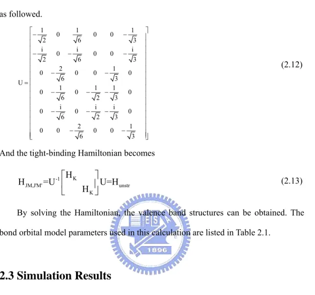
From the coupling coefficients, the JMJ unitary transformation matrix can be obtained as followed. 1 1 1 0 0 0 2 6 3 i i i 0 0 0 2 6 3 2 1 0 0 0 0 6 3 U 1 1 1 0 0 0 6 2 3 i i i 0 0 6 2 3 − − − − − − − = − − − − − − 0 2 1 0 0 0 0 6 3 ⎡ ⎤ ⎢ ⎥ ⎢ ⎥ ⎢ ⎥ ⎢ ⎥ ⎢ ⎥ ⎢ ⎥ ⎢ ⎥ ⎢ ⎥ ⎢ ⎥ ⎢ ⎥ ⎢ ⎥ ⎢ ⎥ ⎢ ⎥ ⎢ ⎥ ⎢ − − ⎥ ⎢ ⎥ ⎢ ⎥ ⎣ ⎦ (2.12)
And the tight-binding Hamiltonian becomes
K -1 JM,J'M' unstr K H H =U U=H H ⎡ ⎤ ⎢ ⎥ ⎣ ⎦ (2.13)
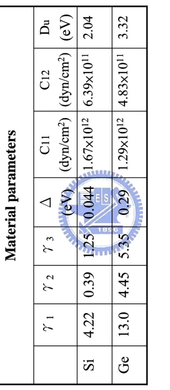
By solving the Hamiltonian, the valence band structures can be obtained. The bond orbital model parameters used in this calculation are listed in Table 2.1.
2.3 Simulation Results
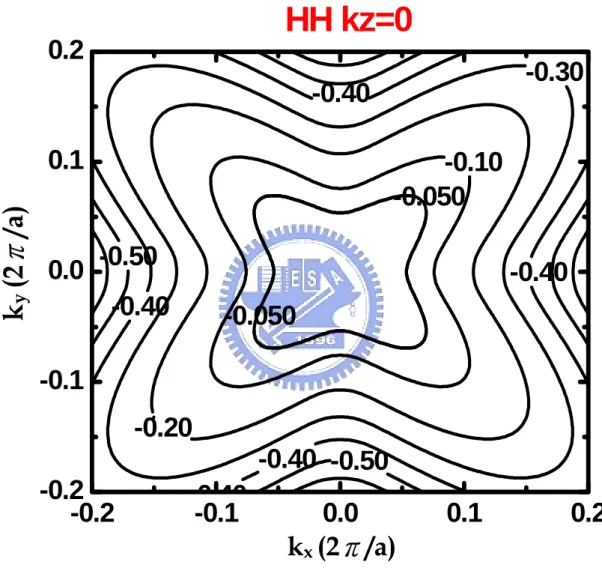
Fig. 2.1 shows the calculated valence band structures, heavy hole (HH) ,light hole (LH) ,and split off(SO) bands, in bulk silicon on (001) substrate from the bond orbital model. The heavy hole and light hole bands are degenerated at the zone center k=(0,0,0). Fig. 2.2 shows the constant energy contour of the heavy hole band on the plane of kz = 0. The strong warping of the heavy hole band is illustrated. The band is
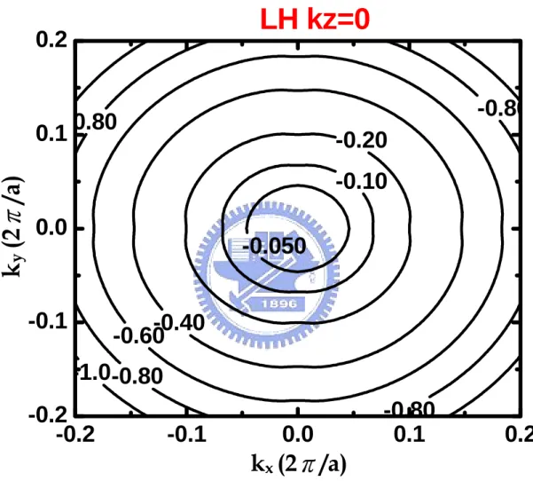
anisotropic, but highly symmetric. Fig. 2.3 shows the constant energy contour of the light hole band on the kz = 0 plane. It has more regular shape compared with the heavy
hole band. The constant energy surfaces for the heavy hole and light hole bands are also plotted in Fig. 2.4 and Fig. 2.5, respectively. The energy is 50meV below the Γ point.
Table 2.1 BO
M materi
al
parame
ter
s for
Si
and Ge
res
pecti
v
el
y
3.32
4.83
×10
111.29
×10
120.29
5.35
4.45
13.0
Ge
2.04
6.39
×10
111.67
×10
120.044
1.25
0.39
4.22
Si
D
u
(eV)
C
12
(dyn/cm
2)
C
11
(dyn/cm
2)
Δ
(eV)
γ
3γ
2γ
1M
a
teri
al
para
m
et
er
s
3.32
4.83
×10
111.29
×10
120.29
5.35
4.45
13.0
Ge
2.04
6.39
×10
111.67
×10
120.044
1.25
0.39
4.22
Si
D
u
(eV)
C
12
(dyn/cm
2)
C
11
(dyn/cm
2)
Δ
(eV)
γ
3γ
2γ
1M
a
teri
al
para
m
et
er
s
-0.6
-0.4
-0.2
0.0
0.2
0.4
0.6
-4
-3
-2
-1
0
[100]
Energy (eV)
Wave Vector, k (2
π
/a)
HH
LH
SO
[110]
Fig. 2.1 Calculated valence band structures on Si (001) substrate from the bond orbital model.
-0.40
-0.40
-0.40
0 40
-0.40
-0.50
-0.50
-0.30
-0.20
-0.10
-0.050
-0.050
-0.2
-0.1
0.0
0.1
0.2
-0.2
-0.1
0.0
0.1
0.2
HH kz=0
Fig. 2.2 The constant energy contour on the kz = 0 plane of the heavy-hole band.
k
y(2
π
/a
)
k
x(2π/a)
-1.0-0.80
0.80
-0.80
-0.80
-0.60
-0.40
-0.20
-0.10
-0.050
-0.2
-0.1
0.0
0.1
0.2
-0.2
-0.1
0.0
0.1
0.2
LH kz=0
Fig. 2.3 The constant energy contour on the kz = 0 plane of the light-hole band.
k
x(2π/a)
k
y(2
π
/a
)
Fig. 2.4 Constant energy surface for the heavy-hole band. The energy is 50meV below the Γ point.
Fig. 2.5 Constant energy surface for the light-hole band. The energy is 50meV below the Γ point.
Chapter 3
Valence Band Structure Calculation –
Luttinger-Kohn Model
3.1 Introduction
In chapter 2, a bond orbital model is employed to calculate the valence band structures of the bulk silicon. In order to take into account the effect of uniaxial compressive strain, a Luttinger-Kohn model is used. This model is similar to the k.p method. The strain effects can be included by the Bir-Pikus deformation potentials. The Luttinger-Kohn model is described as follows.
3.2 Luttinger-Kohn Model
Based on the theory of Luttinger-Kohn [25] and Bir-Pikus [26], the valence band structure of strained semiconductor can be described by the following 6 × 6 Hamiltonian + + + + + + 1 P+Q S R 0 S 2R 2 3 S P Q 0 R 2Q S 2 3 R 0 P Q S S 2Q 2 H= 0 R S P+Q 2R − − − − − − − − + + + + 3, 3 2 2 3 1 , 2 2 3 1 , 2 2 3 3 1S , 2 2 2 1 1 1S 2Q 3S 2R P+ 0 , 2 2 2 2 1 1 3 1 , 2R S 2Q S 0 P+ 2 2 2 2
⎡ ⎤ ⎢ ⎥ ⎢ ⎥ ⎢ ⎥ ⎢ ⎥ ⎢ ⎥ ⎢ ⎥ − ⎢ ⎥ ⎢ ⎥ ⎢ ⎥ − − ⎢ ⎥ ⎢ ⎥ ⎢ ⎥ ⎢− − − ⎥ ⎢ ⎥ ⎢ ⎥ ⎢ − ⎥ − ⎢ ⎥ ⎣ ⎦ + + (3.1) Where k ε P=P +P (3.2)
k ε Q=Q +Q k ε R=R +R k ε S=S +S 2 2 2 2 k 1 x y z 0 P =( ) γ (k +k +k ) 2m 2 2 2 2 k 2 x y z 0 Q =( ) γ (k +k -2k ) 2m 2 2 2 k 2 x y 3 x y 0 R =( ) 3 [ γ (k k )+2iγ k k ] 2m − − 2 k 3 x y z 0 S =( ) 2 3 γ (k ik )k 2m − ε v xx yy zz P = a (ε +ε +ε )− ε xx yy zz b Q = (ε +ε 2ε ) 2 − − ε xx yy xy 3 R = b(ε ε ) idε 2 − − − ε zx yz S = d(ε− −iε )
where is the spin orbit splitting, γ△ 1, γ2, and γ3 are the Luttinger parameters, av, b,
and d are the Bir-Pikus deformation potentials. The parameters used in this thesis are listed in Table 3.1[27]. Moreover, εij is the strain tensor and |j, m> is the Bloch wave
function at zone center and can be written as
3 3 1 , = (x+iy) 2 2 2 3 1 1 , = (x+iy) +2z 2 2 6 3 1 1 , = (x iy) +2z 2 2 6 3 3 1 , = (x iy) 2 2 2 1 1 1 , = (x+iy) +z 2 2 3 1 1 1 , = (x iy) z 2 2 3 − ↑ − ↓ ↑ − − ↑ ↓ − − ↓ ↓ ↑ − − ↑ − ↓
(3.3)
Hamiltonian. In order to obtain a proper six-order determinant equation, it is useful to work on a different basis set
1 ( x + i y ) 2 1 ( x i y ) 2 z 1 ( x i y ) 2 1 ( x + i y ) 2 z ↑ − ↑ ↑ − ↓ ↓ ↓
(3.4)
With this new basis set, the unitary transformation matrix U can be obtained.
1 0 0 0 0 0 2 1 0 0 0 0 3 3 1 2 0 0 0 0 3 3 U 0 0 0 1 0 0 1 2 0 0 0 0 3 3 2 1 0 0 0 0 3 3 − ⎡ ⎤ ⎢ ⎥ ⎢ − ⎥ ⎢ ⎥ ⎢ ⎥ ⎢ ⎥ ⎢ ⎥ = ⎢ ⎢ ⎢ ⎢ ⎢ ⎢ ⎢ − ⎢⎣ ⎦ ⎥ ⎥ ⎥ ⎥ ⎥ ⎥ ⎥ ⎥ (3.5)
The original Hamiltonian H needs to transform into a new Hamiltonian H’
-1 H ' = U HU 3 P+Q 3R S 0 0 0 2 2 3 2 3 P+Q+ S 0 0 3 2 3 2 2 2 S S P 2Q+ 0 3 3 3 = R+ + + − − − − −
+
+
+
+
0 3 3 0 0 0 P+Q 3 2 2 2 3 0 0 3 P+Q+ S 3 3 2 2 3 0 0 S 3 2R S R + + − − −
+
+
+
3 S P 2Q+ 2 3 + ⎡ ⎤ ⎢ ⎥ ⎢ ⎥ ⎢ ⎥ ⎢ ⎥ ⎢ ⎥ ⎢ ⎥ ⎢ ⎥ ⎢ ⎥ ⎢ ⎥ ⎢ ⎥ ⎢ ⎥ ⎢ ⎥ ⎢ ⎥ ⎢ ⎥ ⎢ ⎥ ⎢ − ⎥ ⎢ ⎥ ⎣ ⎦+
(3.6)1 1 1 2 1 3 2 2 1 2 2 2 3 1 1 1 2 1 3 3 1 3 2 3 3 2 2 1 2 2 2 3 1 1 1 1 2 1 3 1 3 1 3 2 3 3 1 2 2 2 3 2 1 3 2 3 3 3 a a a 0 0 0 a a a 0 0 x a a a a a a 0 - x 0 = a a a a x 0 0 0 a a a a a a 0 0 - x a a a 0 x 0 a a a ⎛ ⎞ ⎜ − ⎟ ⎜ ⎟ ⎜ ⎟ ⎝ ⎠ (3.7)
the six-order determinant equation can be simplified to a square of a cubic equation as followed. 3 2 2 ij ij det(H' −δ E) {ε= ++ε −3λε [µ− ++λ]} =0 (3.8) where 2 2 2 3 2 2 2 + +2 ε=E+P, λ=Q +|S| +|R| , 3 3 µ=2Q +3Q|S | 6Q|R | (S R +S R) 2 − +
The valence band structures can then be obtained by solving the cubic eigen-equation analytically.
3.3 Simulation Results
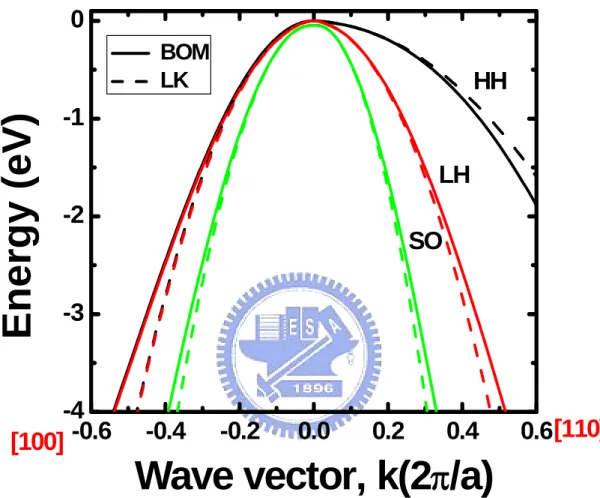
For the unstrained case, Fig. 3.1 shows the valence band structures in bulk silicon from the bond orbital model (BOM, solid lines) and from the Luttinger-Kohn model (dash lines). Apparently, those two models have a significant deviation in the high energy portion. For the heavy hole band along [100] direction, the energy from the Luttinger-Kohn model is 10% larger than that from the bond orbital model at wave vector k=0.3*(2π/a).
For the strained case, Fig. 3.2 and Fig. 3.3 show the valence band structures under uniaxial compressive strain along [100] and [110] directions with ε= -0.5%,
which ε is defined as 0
0
a a
a −
,where a is the lattice constant with strain, and a0 is the
for the top band and second band are splited due the applied uniaxial compressive. This energy splitting is important for the reduction of the interband phonon scattering [28].The presence of anti-crossings are found, which are defined as the lowest lying hole band/highest lying valence band [29]. In Fig. 3.4 and Fig. 3.5, the constant energy surfaces of top band on the kz = 0 plane under uniaxial compressive strain
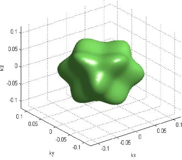
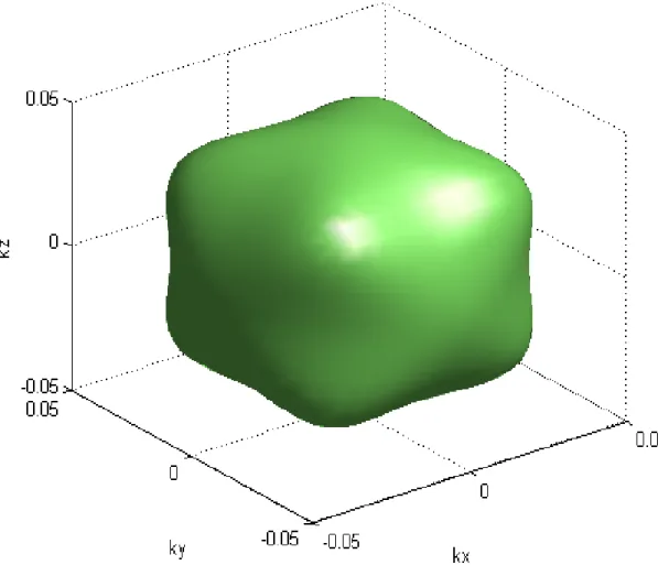
along [100] and [110] directions with ε= -0.5% are plotted. The symmetry of the top band is broken, which results in a redistribution of holes in k-space. On the other hand, the conduction effective masses alone the strain directions become smaller, which gives rise to the mobility enhancement. The mobility calculation is based on a Monte Carlo simulation and will be given in detail in chapter 4. The constant energy surfaces for the top band under uniaxial compressive strain along [100] and [110] directions with ε= -0.5% are also plotted in Fig. 3.6 and Fig. 3.7. The energy is 30meV below the Γ point.
-5.50
-2.55
1.24
0.29
5.35
4.45
13.0
Ge
-5.32
-2.35
2.46
0.044
1.25
0.39
4.22
Si
d
(eV)
b
(eV)
a
v(eV)
Δ
(eV)
γ
3γ
2γ
1Material paramet
ers
-5.50
-2.55
1.24
0.29
5.35
4.45
13.0
Ge
-5.32
-2.35
2.46
0.044
1.25
0.39
4.22
Si
d
(eV)
b
(eV)
a
v(eV)
Δ
(eV)
γ
3γ
2γ
1Material paramet
ers
T
a
ble 3.
1
L
uttiger
-K
ohn
parame
ters and Bir-Pi
kus
deformati
o
n
poten
ti
a
ls
for
Si
and Ge
res
pecti
v
el
y
-0.6
-0.4
-0.2
0.0
0.2
0.4
0.6
-4
-3
-2
-1
0
[100]
Energy (eV)
Wave vector, k(2
π
/a)
BOM
LK
HH
LH
SO
[110]
Fig. 3.1 Calculated valence band structures on Si (001) substrate from the bond orbital model (BOM, solid lines) and from the Luttinger-Kohn model (dash lines).
-0.15 -0.10 -0.05 0.00
0.05
0.10
0.15
-0.6
-0.5
-0.4
-0.3
-0.2
-0.1
0.0
[110]
En
erg
y
(
e
V)
Wave Vector ,k
(
2
π
/a
)
E1
E2
E3
[100]
Fig. 3.2 Valence band structures, top band (E1), second band (E2) ,and split-off band(E3), under uniaxial compressive strain along [100] channel direction at ε= -0.5%.
-0.15 -0.10 -0.05 0.00
0.05
0.10
0.15
-0.6
-0.4
-0.2
0.0
[100]
Energy
(eV
)
Wave vector, k
(
2
π/
a
)
E1
E2
E3
[110]
Fig. 3.3 Valence band structures, top band (E1), second band (E2) ,and split-off band(E3), under uniaxial compressive strain along [110] channel direction at ε= -0.5%.
-0.40
-0.40
-0.40
-0.40
-0.50
-0.50
-0.50
-0.50
-0.30
-0.20
-0.10
-0.030
-0.2
-0.1
0.0
0.1
0.2
-0.2
-0.1
0.0
0.1
0.2
Fig. 3.4 Constant energy contour on the kz=0 plane of the top band under
uniaxial stress along [100] channel direction at ε= -0.5%.
k
x(2π/a)
k
y(2
π
/a
)
-0.40
-0.40
-0.40
-0.40
-0.30
-0.30
-0.20
-0.10
-0.030
-0.2
-0.1
0.0
0.1
0.2
-0.2
-0.1
0.0
0.1
0.2
Fig. 3.5 Constant energy contour on the kz=0 plane of the top band under
uniaxial stress along [110] channel direction at ε= -0.5%.
k
x(2π/a)
k
y(2
π
/a
)
Fig. 3.6 Constant energy surface for top band under uniaxial stress along [100] channel direction at ε= -0.5%. The energy is 30meV below the Γ point.
Fig. 3.7 Constant energy surface for top band under uniaxial stress along [110] channel direction at ε= -0.5%. The energy is 30meV below the Γ point.
Chapter 4
Hole Transport Properties in Strained Silicon
4.1 Introduction
Due to a strong coupling of the heavy hole, light hole, and split off bands in silicon, leading to a warping of the constant energy surface, the usual analytical approximations of the valence bands are not suitable for simulating carrier transport. A realistic band structure including the heavy hole, light hole, and split off bands must be adopted. However, the inclusion of the band structure in the Boltzmann transport equation is impractical. The Monte Carlo (MC) method provides an alternative approach to the Boltzmann transport equation [30]. The Monte Carlo method could take into account realistic band structures and a large variety of scattering mechanisms. In this chapter, the hole mobility at low electric fields and the hole velocity at high electric fields will be evaluated with a Monte Carlo simulation.
In order to properly include the high field and high energy transport effects, a bond orbital model is used to calculate the bulk silicon valence band structure, as described in chapter 2, in the Monte Carlo simulation. Moreover, the Luttinger-Kohn model, as described in chapter 3, is also employed to take into account the strain effect. Hole scattering mechanisms in the Monte Carlo simulation include acoustic-phonon, nonpolar optical phonon scattering, and impact ionization. The hole drift velocity is simulated at T=300K.
4.2 Physical Model and Simulation Technique
first step is to identify the scattering potential Us(r) and then to evaluate the matrix element, ik r ik r kk
1
M =
e
Us(r)e
Ω
′ − − ′∫
i i (4.1)where Ω is the volume of a unit cell. From the matrix element, we find the transition rate as:
2 kk kk
2π
W =′ |M | δ(E(k )-E(k)-∆E)′ ′ (4.2) where E is the change in energy caused by collision. The transition rate W△ kk’
represents the probability per unit time that a carrier with momentum k scatters to
a state with momentum k ′. In other words, the transition rate is the rate at which
carriers are scattered from a specific initial state k to a specific final state k’. The major hole scattering mechanism are acoustic phonon scattering, nonpolar optical phonon scattering, and impact ionization. The scattering rates of the mechanism are described below [32]. The acoustic phonon scattering rate is given by
2 b 0 eff ac 2 1 πk T E S = D(E) ρu (4.3)
where Eeff is the effective deformation potential, ρ is the material density, u1 is the
velocity of sound in the material, T0 is lattice temperature and D(E) is the density of
hole states obtained from the realistic valence band structure. The optical phonon scattering rate is 2 t op w b ph b ph πD (i) 1 1
S (i)= [N + ]D(E k T (i))
2ρk T (i) 2 2∓ ± (4.4) w ph 0 1 N = exp(T (i)/T ) 1−
where Dt(i) is the optical phonon coupling constant in the i-th band (i =1,2,3 denote
optical phonon temperature, and Nww is the Bose-Einstein distribution. The + and –
represents the absorption and emission rates. Finally, the impact ionization rate is obtained from the Keldysh formula [33],
2 th impact op th E E S =S (E)p( ) E − (4.5) In the simulation, the scattering parameters used to fit experimental results are Eeff,
Tph(i), Dt(i), Eth and p. Two methods are used in our fitting procedure, the conjugate
gradient method and surface response methods [34]. First, the conjugate gradient method is used, in which the results are assumed to be linearly proportional to the parameters, to give rough values of the parameters. Then, the optimized value can be obtained by using the surface response method, in which, both the simulation and objective function iteratively solved until a self consistent solution is achieved. In above methods, we need to define an objective function:
2 i i i i ˆ (x -x (p)) f(p)= ˆx ⎡ ⎤ ⎢ ⎥ ⎣ ⎦
∑
(4.6)where ˆx represents the experimental values, i x is the simulation values, and p i represents a set of fitting parameters. The values of the scattering parameters are shown in Table 4.1.
In the numerical implementation of the valence band structure obtained from the bond orbital model and Luttinger-Kohn method, tabular forms of the E-k relationship [35] for the lowest three valence bands are established in the simulation. The smallest mesh size in k-space is 0.01(2π/a) in a region near the Γ point. Fig. 4.1 shows a flowchart of a simple Monte Carlo simulation [36]. In the Monte Carlo simulation, a carrier hole is simulated under an external electric field. It travels freely between two successive scatterings. The free-flight time is determined by using a fixed time technique. During the free flight, the hole is accelerated by the field and its
momentum and energy are updated according to the tabular form of the E-k relationship. If a scattering happens, a random number is generated to decide the responsible scattering mechanism and the new hole state is chosen according to the tabular form of the E-k relationship. This procedure is continued until the fluctuation due to the statistical uncertainty is less than 1%.
4.3 Results and Discussions
4.3.1 Unstrained Silicon
Fig. 4.2 shows the density of states obtained from the bond orbital model (solid line) and Luttinger-Kohn method (dash line). The density of states obtained from bond orbital model and Luttinger-Kohn model is different for the high energy. Fig. 4.3 shows the hole optical phonon and acoustic phonon scattering rates as a function of hole energy obtained from the bond orbital model (solid line) and Luttinger-Kohn method (dash line). As can be seen clearly, optical phonon scattering is dominant in the high energy region for both models.
Fig. 4.4 shows the simulated hole energy distribution at electric field of 200kV/cm with the bond orbital model (square) and with the Luttinger-Kohn method (circle). Fig. 4.5 shows the hole drift velocities versus electric field for bulk Si ,Ge and Si0.8Ge0.2. Fig. 4.6, demonstrates the hole drift velocities along [100] and [110]
directions. The drift velocity at electric field of 200kV/cm along the [100] direction is about 10% larger. Moreover, a weak anisotropic behavior of the drift velocity is also observed, similar to [37].
4.3.2 Strained Silicon
In the following part, the strain effect on the mobility is evaluated with the Luttinger-Kohn model. As indicated in [28], to have a good strain induced hole
mobility enhancement, there are four key parameters for valence band structure characteristics, (1) low effective mass along the channel direction to increase mobility, (2) high density of states effective mass to increase the top band occupation probability, (3) high hole energy splitting to reduce the interband phonon scattering and (4) high out-of-plane effective mass. Table 4.2 shows the calculated effective mass and energy splitting levels in different stressors, -0.5% compressive strain in [100] and [110] directions, compared to [100] direction without applied strain. As can be seen clearly, compressive strain induced effective mass reduction in channel direction and energy splitting can be observed. In addition, compared to [100] direction, effective mass in [110] direction is moderately decreased, which is consistent with the piezoresistance concept [38]. From the piezoresistance concept, on (001) wafer, the value of π|| in [110] direction is larger than in [100] direction.
Fig. 4.7 shows phonon scattering rate for the unstrained and strained case with ε= -0.5% along different directions, [100] (dash line) and [110] (dot line). The strain effect on hole transport is manifested in a slight reduction of the optical phonon scattering rate, which is attributed to the splitting of the heavy hole and light hole bands. Moreover, the phonon scattering rate in [110] direction is smaller than in [100] direction with applied uniaxial compressive strain due to larger energy splitting. In Fig. 4.8, hole drift velocity as a function of the electric field applied along the [100] direction for two unaixial compressive strain cases, ε= 0, and -0.5%, is shown, respectively. One point is worth mentioning. The uniaxial compressive stress direction is along channel direction. In Fig. 4.8, the low field mobility is extracted in the inset. Finally, Fig. 4.9 shows the extracted low field mobility along [100] and [110] directions with different stressors. And the simulation results show that the hole mobility enhancement is increased with larger uniaxial compressive strain, which consists with the experiment results as published in [39]. Furthermore, the strain
induced mobility enhancement in [110] channel direction is larger than in [100] direction.
0.
004
1.
6
280
340
440
24.0
11
.0
8.8
10.8
Ge
0.
002
1.
7
440
490
540
8.7
8.
8
8.9
4.4
Si
(eV)
(K
)
(10
8eV
/cm
)
(eV)
p
E
th
T
ph
(3)
T
ph
(2)
T
ph
(1)
D
t
(3
)
D
t
(2)
D
t
(1
)
E
ef
f
Scatte
ri
ng
Pa
ram
eters
0.
004
1.
6
280
340
440
24.0
11
.0
8.8
10.8
Ge
0.
002
1.
7
440
490
540
8.7
8.
8
8.9
4.4
Si
(eV)
(K
)
(10
8eV
/cm
)
(eV)
p
E
th
T
ph
(3)
T
ph
(2)
T
ph
(1)
D
t
(3
)
D
t
(2)
D
t
(1
)
E
ef
f
Scatte
ri
ng
Pa
ram
eters
Table 4.1
Scattering para
meters us
ed
in the Monte
Car
lo
si
mulation for
Si
an
d G
e
r
esp
ec
ti
vely.
m
x(m
0)
ε= 0
[100]
0.29
0.29
0.19
0.23
ε= -0.5%
[100]
ε= -0.5%
[110]
0.13
0.38
stressors
m
DOS(m
0)
∆ (meV)
0.0
28.1
33.8
m
z(m
0)
0.29
0.28
0.28
Table 4.2 Calculated effective mass and energy splitting levels in different stressors, -0.5% compressive strain in [100] and [110] directions, and
Fig. 4.1 Flowchart of a typical Monte Carlo program.
Initialize physical constant, E-scattering table
Calculate E and K
Determine flight time
Select scattering mechanism
Determine final state
Calculate new E’ and K’
Print results
Scattering?
No Yes
0.0
0.5
1.0
1.5
2.0
1E20
1E21
1E22
DO
S (eV
-1
cm
-3
)
Energy (eV)
BOM
LK
Fig. 4.2 Density of states in bulk silicon from the bond orbital model (solid line) and from the Luttinger-Kohn model (dash line).
0.0
0.5
1.0
1.5
2.0
1E12
1E13
1E14
1E15
op(abs.)
ac(abs.)
ac(emi.)
Scattering R
a
te
(1
/
sec
)
Hole Energy (eV)
BOM
LK
op(emi.)
Fig. 4.3 Scattering rates of hole scattering mechanisms in bulk silicon from the bond orbital model (solid line) and from the Luttinger-Kohn model (dash line).
0
1
2
3
4
10
010
110
210
3Dis
tr
ibution (ar
b
. uni
t)
Hole Energy (ev)
BOM
LK
Fig. 4.4 Hole energy distributions calculated from the bond orbital model (square) and from the Luttinger-Kohn model (circle) at the electric field of 200 kV/cm.
1
10
100
10
610
7Ho
le Velo
city (cm/s)
Field (kV/cm)
Ge
Si
Si0.8Ge0.2
Fig. 4.5 Calculated hole drift velocity as a function of electric field for bulk Si, Ge and Si0.8Ge0.2.
1
10
100
10
610
7H
ole
Ve
loc
ity (c
m/s
)
Field (kV/cm)
[100]
[110]
Fig. 4.6 Hole drift velocity as a function of the electric field along [100] and [110] directions.
0.0
0.1
0.2
0.3
1x10
142x10
14Scattering Rate (1/sec)
Hole Energy (eV)
unstrain
strain [100]
strain [110]
Fig. 4.7 Optical phonon scattering rate for uniaxial compressive strain with ε= -0.5% in the [100] (dash line) and [110] (dot line) directions, compared with unstrained case (solid line).
1
10
100
10
610
7Hole Velocity (cm/s)
Field (kV/cm)
ε=0
ε=−0.5%
Fig. 4.8 Hole drift velocity as a function of the electric field applied along [100] direction for two uniaxial compressive strain cases, ε= 0, and -0.5%. The uniaxial compressive strain direction is the channel direction. The low field mobility is extracted in the inset.
0 1 2 3 0.0 5.0x10⁵ 1.0x10⁶ 1.5x10⁶ 2.0x10⁶ H o le Velo ci ty (c m/s ) Field (kV/cm) ε=0 ε=−0.5%
0.0
-0.1
-0.2
-0.3
-0.4
-0.5
400
500
600
M
o
bil
ity (cm
2
/v*sec)
strain (%)
[100]
[110]
Fig. 4.9 Calculated hole mobility versus uniaxial compressive stress along [100] and [110] directions.
Chapter 5
Conclusions
Two kinds of valence band structure models are studied. A Monte Carlo simulation is developed to calculate hole transport properties, such as hole mobility and drift velocity. Moreover, the difference of the simulation results with the bond orbital model and with the Luttinger-Kohn model is also examined. Furthermore, the hole drift velocities along [100] and [110] channel directions are also calculated, and the simulation results show the weak anisotropy of the drift velocity.
The strain effect on hole mobility is also evaluated with the Luttinger-Kohn model. And our simulation results show that the hole mobility enhancement can be obtained with uniaxial compressive strain. And it draws a lot of interest to apply compressive strain in [110] direction due to its larger mobility enhancement.
Finally, a Monte Carlo program is established to simulate the carrier transport properties. The strain effect on the device performance, such as mobility and saturation velocity can be examined by a Monte Carlo program, which will becomes a powerful simulation tool for device simulation in the next generation.
Reference
[1] P. Bai C. Auth, S. Balakrishnan, M. Bost, R. Brain, V. Chikarmane, R. Heussner, M. Hussein, J. Hwang, D. Ingerly, R. James, J. Jeong, C. Kenyon, E. Lee, S.H. Lee, N. Lindert, M. Liu, Z. Ma, T. Marieb, A. Murthy, R. Nagisetty, S. Natarajan,
J. Neirynck, A. Ott, C. Parker, J. Sebastian, R. Shaheed, S. Sivakumar, J.
Steigerwald, S. Tyagi, C. Weber, B. Woolery, A. Yeoh, K. Zhang, and M. Bohr, “A 65 nm logic technology featuring 35 nm gate lengths, enhanced channel strain, 8 Cu interconnects layers, low-k ILD and 0.57 um2 SRAM cell,” in Tech. Dig. IEEE Int. Electron Devices Meeting, pp. 657–660, 2004.
[2] P.R. Chidambaram, B.A. Smith, L.H Hall, H. Bu, S. Chakravarthi, Y. Kim, A.V. Samoilov, A.T. Kim, P.J. Jones, R.B. Irwin, M.J Kim, A.L.P Rotondaro, C.F Machala, and D.T. Grider, “35% drive current improvement from recessed-SiGe drain extensions on 37 nm gate length PMOS,” in Proc. Symp. VLSI Technology,
pp. 48–49, 2004.
[3] T. Ghani, M. Armstrong, C. Auth, M. Bost, P. Charvat, G. Glass, T. Hoffiann', K. Johnson', C. Kenyon, J. Klaus, B.Mclntyre, K. Mistry, A. Murthy, 1. Sandford, M. Silberstein, S. Sivakumar, P. Smith, K. Zawadzki, S. Thompson andM. Bohr. “A 90 nm high volume manufacturing logic technology featuring novel 45 nm gate length strained silicon CMOS transistors,” in IEDM Tech. Dig.,
pp.11.6.1–11.6.3, 2003.
[4] V. Chan, R. Rengarajan, N. Rovedo, W. Jin, T. Hook, P. Nguyen, J. Chen, Ed Nowak, X. D. Chen, D. Lea, A. Chakravani, V. Ku, S. Yang, A. Steegen, C. Baiocco, P. Shafer, H. Ng, S. F. Huang, C. Wann. “High speed 45 nm gate length CMOSFETs integrated into a 90 nm bulk technology incorporating strain engineering,” in IEDM Tech. Dig., pp. 3.8.1–3.8.4, 2003.
[5] C. Chien-Hao, T. L.Lee, T. H. Hou, C. L. Chen, C. C. Chen, J. W. Hsu, K. L. Cheng, Y. H. Chiu, H. J. Tao, Y. Jin, C. H. Diaz et al., “Stress memorization technique (SMT) by selectively strained-nitride capping for sub-65 nm
high-performance strained-Si device application,” in VLSI Symp. Tech. Dig., pp.
56–57, 2004.
J. Klaus, Ma Zhiyong, B. Mcintyre, A. Murthy, B. Obradovic, L. Shifren, S. Sivakumar, S. Tyagi, T. Ghani, K. Mistry, M. Bohr, and Y. El-Mansy, “A logic nanotechnology featuring strained silicon,” IEEE Electron Device Lett., vol. 25, pp. 191–193, 2004.
[7] S. Ito, H. Namba, K. Yamaguchi, T. Hirata, K. Ando, S. Koyama, S. Kuroki, N. Ikezawa, T. Suzuki, T. Saitoh, and T. Horiuchi., “Mechanical stress effect of etch-stop nitride and its impact on deep submicrometer transistor design,” in IEDM Tech. Dig., pp. 247–250, 2000.
[8] W. Kohn and J. M. Luttinger, “Quantum theory of electrical transport phenomena,” Phys. Rev, vol.108, pp. 590, 1957.
[9] K. K. Thornber, “High field electronic conduction in insulator,” Solid State Electron, vol.21, pp.259, 1978.
[10] K. Blotekjaer, “Transport equations for electrons in two-valley semiconductors”, IEEE Trans. Electron devices, vol.17, pp.39, 1970.
[11] R. K. Cool and J. Frey, “Two dimensional numerical simulation of energy transport effect in Si and GaAs MESFETs.” IEEE Trans. Electron Devices, vol.29, pp. 970, 1982
[12] Y. C. Chang, “Bond-orbital models for superlattices,” Phys. Rev. B, vol.37, pp. 8215-8222, 1988.
[13] C. Y. P. Chao, S. L. Chuang, ”Spin-orbit-coupling effects on the valence band structure of strained semiconductor quantum wells,” Phys. Rev. B, vol.46, pp. 4110-4122, 1992.
[14] M. L. Cohen and T. K. Bergstresser, “Band structures and pseudopotential form factors for fourteen semiconductors of the diamond and zinc-blende structures,” Phys. Rev., vol.141, pp.789,1966.
[15] J. R. Chelikowsky and M. L. Cohen, “Nonlocal pseudopotential calculations for the electronic structure of eleven diamond and zinc-blende semiconductors” Phys. Rev. B, vol.14, pp.556,1976.
[16] G.Ottaviani, L. Reggiani, C.Canali, F. Nava, and A. Alberigi-Quaranta, “Hole drift velocity in silicon,” Phys. Rev. B, vol.12, pp.3318-3329,1975.
[17] S. Krishnamurthy and J. A. Moriarty, “Electronic structure and impurity-limited electron mobility of silicon superlattices,” Phys. Rev. B, vol.32, pp.1027,1985. [18] W. A. Harrison, “Bond orbital model and the properties of Tetrahedrally
[19] J. C. Slater and G. F. Koster, “Simplified LCAO method for the periodic potential problem,” Phys. Rev., vol.94, pp.1498, 1954.
[20] E. O. Kane, “Energy bans structure in p-type germanium and silicon,” J. Phys. Chem. Solid, vol.1, pp. 82, 1954.
[21] J. Y. Tang and K. Hess, “Impact ionization of electrons in silicon (steady state),” J. Appl. Phys., vol.54, pp.5139, 1983.
[22] P. Lawaetz, “Valence-band parameters in cubic semiconductors,” Phy. Rev. B, vol.4, pp.3460, 1971.
[23] J. C. Hensel and K. Suzuki, “Cyclotron resonance experiments in uniaxially stressed silicon: valence band inverse mass parameters and deformation potential,” Phys. Rev., vol.129, pp.1041,1963.
[24] G. Dresselhaus, A. F. Kip, and C. Kittel, “Cyclotron resonance of electrons and holes in silicon and germanium crystals,” Phys. Rev., vol.98, pp.368, 1955. [25] J.M. Luttinger, “Quantum Theory of Cyclotron Resonance in
Semiconductors: General Theory ”, Phys. Rev. ,vol.102, pp.1030-1041,1956. [26] G. L. Bir and G. E. Pikus, Symmetry and strain-induced Effects in
Semiconductors, Wiley New York, 1974
[27] CG Van de Walle, “Band lineups and deformation potentials in the model-solid theory”, Phys. Rev. ,vol.39, pp. 1871-1883,1989
[28] SE Thompson, G. Sun, Y. S. Choi, and T. Nishida , “Uniaxial-Process-Induced Strained-Si:Extending the CMOS Roadmap”, IEEE Transactions on electron devices, vol.53, pp. 1010-1020, 2006
[29] X.F. Fan, L. F. Register, B. Winstead, M. C. Foisy, ,W. Chen, X. Zheng, B. Ghosh, and S. K. Banerjee, “Hole Mobility and Thermal Velocity
Enhancement for Uniaxial Stress in Si up to 4 GPa”, IEEE Transactions on electron devices, vol.54, pp. 291-296, 2007.
[30] W. Fawcett, A. D. Boardman, and S. Swain, “Monte Carlo determination of electron transport properties in gallium arsenide,” J PHYSICS CHEM SOLIDS, vol.31, pp.1963, 1970.
[31] M. Lundstrom,”Modular Series on Solid State Devices Vol. X: Fundamentals of Carrier Transport,” Purdue University press, pp.35, 1990.
[32] T. Manku and A. Nathan, “Lattice mobility of holes in strained and unstrained Si1-xGex alloys,” IEEE Electron Device Lett., vol.12, pp.704, 1991.
[33] L. V. Keldysh, “Concerning the theory of impact ionization semiconductors,” Sov. Phys. JETP, vol.21, pp.1135, 1965.
[34] Goulb and Van Loan, Matrix Computation, The Johons Hopkins University press, 1989.
[35] M. V. Fischetti and D. J. DiMaria, “Quantum Monte Carlo Simulation of
high-field electron transport: an application to silicon dioxide,” Phys. Rev. Lett., vol.55, pp.2475, 1985.
[36] C. Jacoboni and L. Reggiani, “The Monte Carlo method for the solution of charge transport in semiconductors with applications to covalent materials,” Rev. Mod. Phys., vol.55, pp.645, 1983.
[37] F. M. Bufler, A. Tsibizov, and A. Erlebach, “Scaling of Bulk pMOSFETs: (110) Surface Orientation Versus Uniaxial Compressive Stress,” IEEE Electron Device Lett., Vol. 27, pp. 992-994, 2006.
[38] Yozo Kanda, “A Graphical Representation of the Piezoresistance Coefficients in Silicon,” IEEE Transactions on electron devices, Vol.29, pp. 64-70, 1982. [39] K. Mistry, M. Armstrong, C. Auth, S. Cea, T. Coan, T. Ghani, T. Hoffmann, A.
Murthy, J. Sandford, R. Shaheed, K. Zawadzki, K. Zhang, S. Thompson, and M. Bohr, “Delaying forever: Uniaxial strained silicon transistors in a 90 nm CMOS technology,” in Symp. VLSI Tech. Dig., pp. 50–51, 2004.

![Fig. 3.2 Valence band structures, top band (E1), second band (E2) ,and split-off band(E3), under uniaxial compressive strain along [100] channel direction at ε= -0.5%](https://thumb-ap.123doks.com/thumbv2/9libinfo/8251745.171722/31.892.143.753.287.826/valence-structures-second-uniaxial-compressive-strain-channel-direction.webp)
![Fig. 3.3 Valence band structures, top band (E1), second band (E2) ,and split-off band(E3), under uniaxial compressive strain along [110] channel direction at ε= -0.5%](https://thumb-ap.123doks.com/thumbv2/9libinfo/8251745.171722/32.892.136.741.300.837/valence-structures-second-uniaxial-compressive-strain-channel-direction.webp)
