國
立
交
通
大
學
電子工程學系 電子研究所
碩 士 論 文
利用準分子及連續波雷射退火製作高效能低溫複晶
矽薄膜電晶體之研究
Study on High-Performance Low-Temperature
Poly-Silicon Thin Film Transistors with Excimer and
Continuous-Wave Laser Annealings
研 究 生:陳旭信
Hsu-Hsin Chen
指導教授:鄭晃忠 博士
Dr. Huang-Chung Cheng
利
利
用
用
準
準
分
分
子
子
及
及
連
連
續
續
波
波
雷
雷
射
射
退
退
火
火
製
製
作
作
高
高
效
效
能
能
低
低
溫
溫
複
複
晶
晶
矽
矽
薄
薄
膜
膜
電
電
晶
晶
體
體
之
之
研
研
究
究
Study on High-Performance Low-Temperature Poly-Silicon Thin Film
Transistors with Excimer and Continuous-Wave Laser Annealings
研 究 生
: 陳旭信 Student : Hsu-Hsin Chen
指導教授
: 鄭晃忠 博士 Advisor : Dr. Huang-Chung Cheng
國立交通大學
電子工程學系 電子研究所
碩士論文
A Thesis
Submitted to Department of Electronics Engineering
& Institute of Electronics
College of Electrical and Computer Engineering
National Chiao-Tung University
In Partial Fulfillment of the Requirements
for the Degree of Master
in
Electronics Engineering
2006
Hsinchu, Taiwan, Republic of China
中華民國 九十五 年 七 月
利用準分子及連續波雷射退火製作高效能低溫複晶矽薄膜
電晶體之研究
研究生:陳旭信 指導教授:鄭晃忠 博士
國立交通大學
電子工程學系 電子研究所碩士班
摘要
近年來,低溫複晶矽薄膜電晶體是在顯示技術應用中的關鍵元件。雖然透過準分子 雷射可有效的提升頂閘極低溫複晶矽薄膜電晶體複晶矽層的結晶性,但此方法仍有此許 缺點,如它可能在主動層和介電層之間造成大的粗糙界面,也可能形成隨機的晶界分佈 等等。在這篇論文裡,我們將提出三種方法來增進低溫複晶矽薄膜電晶體的特性。 在第一個部分,我們稱為位置控制單垂直晶界低溫複晶矽薄膜電晶體方法將被提出 而加以探討。我們將介紹單晶界低溫複晶矽薄膜電晶體機制。因為底閘極結構邊緣台階 區提供了較厚非晶矽層,在準分子雷射退火時表示出晶種的特性。當雷射能量密度控制 使得較薄的元件通道區域全熔,且接近角落較厚的區域半熔,如此一來,由通道二邊側向成長的晶粒沿著相反的方向向通道中間成長,進而在通道的中心只形成一條垂直的晶 界。因此,我們可以得到大型的晶粒,進而提升元件的效能。各種各樣的分析方法也將 用來探討單垂直晶界低溫複晶矽薄膜層,由掃描式電子顯微鏡,穿透式電子顯微鏡和原 子力顯微鏡的分析中可知,我們觀察到大約 0.75μm長的人工控制晶粒。 我們也加以研究了單垂直晶界低溫複晶矽薄膜電晶體的電特性,可完全與傳統底閘 極低溫複晶矽薄膜電晶體製作流程相容的單垂直晶界低溫複晶矽薄膜電晶體將被製作 出來,在沒有任何氫化的處理之下,其載子移動率更超過 250cm2 / V-s。我們也觀察到 閘極引起的汲極漏電和紐結效應也減少了,同樣的元件的均勻性也被提升,在量測二十 個元件之下,載子移動率的標準差小於30cm2 /V*s ,臨界電壓的標準差小於0.5 V。而且 在沒有任何可靠度衰退之下(如在傳統的頂閘級元件中較低的崩潰電場),單垂直晶界 低溫複晶矽薄膜電晶體更適用於較薄的閘極氧化層。因此,高性能單垂直晶界低溫複晶 矽薄膜電晶體可在無任何特殊結構和材料的條件下單純利用較薄的閘極氧化層得到更 佳的元件驅動能力與更陡直的的次臨界擺幅。 雖然單垂直晶界低溫複晶矽薄膜電晶體表現出良好的電特性,由於偏離的離子佈植 使得不對稱的電特性成為其一大問題。因此在第二個部分中,我們將結合單垂直晶界低 溫複晶矽薄膜電晶體方法與背後曝光法製作出新穎自我對準的單垂直晶界低溫複晶矽 薄膜電晶體。非晶矽閘極層形成了如同光罩的效果,在微影製程下阻擋了來自於汞燈的 紫外光,從光學顯微鏡和掃描式電子顯微鏡的分析中可看出,光阻可完美自我對準於非 晶矽閘極層。除了單垂直晶界低溫複晶矽薄膜電晶體原本具有的良好特性外,自我對準 的單垂直晶界低溫複晶矽薄膜電晶體也表現出對稱性良好的電特性。自我對準單垂直晶 界低溫複晶矽薄膜電晶體載子遷移率可大約192 cm2 / V-s而在同樣的製程條件下的非自 我對準元件卻大約只有 17.76 cm2 / V-s。閘極引起的汲極漏電和紐結效應也減少了。 如此一來我們更能將自我對準的單垂直晶界低溫複晶矽薄膜電晶體應用於畫素電路中 的開關元件。 可惜的是,在自我對準的單垂直晶界低溫複晶矽薄膜電晶體的通道中仍然有一垂直 晶界。因此,新穎連續波雷射結晶法在本論文的第三部分被提出。首先,我們先探討了
連續波雷射在摻雜活化的特性,我們發現以連續波雷射活化是一個低熱預算和高效率方 法。其活化能力可使片電阻低於 47 Ω/□。接下來,我們也用連續波雷射結晶法製作 出高效能 n 型和 p 型的低溫複晶矽薄膜電晶體。根據以前的研究中指出,利用連續波結 晶法晶界將和雷射掃描的方法平行。如此一來,使用連續波雷射結晶法可製作出無高角 度晶界的低溫複晶矽薄膜電晶體,而載子移動率在 n 型和 p 型中分別為 192 cm2 /V-s 和 92 cm2 /V-s。另一方面,由於可完全與傳統頂閘極低溫複晶矽薄膜電晶體製作流程相容, 因此製作流程十分簡單。加上由於連續波雷射結晶法掃描的速度很快,使得連續波結晶 法低溫複晶矽薄膜電晶體的產出率上升,因此十分適合將來系統面板的應用 。
Study on High-Performance Low-Temperature
Poly-Silicon Thin Film Transistors with Excimer and
Continuous-Wave Laser Annealings
Student : Hsu-Hsin Chen Advisor : Dr. Huang-Chung Cheng
Department of Electronics Engineering & Institute of Electronics
National Chiao Tung University
ABSTRACT
In recent years, low temperature polycrystalline thin film transistors (LTPS-TFTs) were the key devices in display applications. Although conventional top-gate LTPS-TFTs by excimer laser crystallization was an effective technology in improving the crystallinity of polycrystalline silicon thin films, there were still some drawbacks in conventional top-gate LTPS-TFTs such as high roughness interface between active layer and gate insulator, random grain boundaries and etc. In this thesis, we introduced three methods to improve the performance of LTPS-TFTs.
In the first part, the methods called location-controlled vertical single grain-boundary (VSGB) low temperature poly silicon (LTPS) thin films transistors with bottom gate (BG) structures fabricated by excimer laser annealing were investigated. The mechanisms of VSGB-LTPS thin film were studied. A thick amorphous silicon region was formed in the
corner due to the step structures of bottom gate which they served as the seeds for lateral grain growth during excimer laser irradiation. The laser energy density must be controlled to completely melt the thin region in the channel and partially melt the thick region near the corner. In addition, the lateral grain growth starting from channel edge could progress along the opposite direction toward the center of channel region. There was only one longitudinal boundary in the center of the channel. Thus, a large-grain polycrystalline silicon film was obtained which would lead to improved device performance. Various analyses were performed to investigate VSGB-LTPS thin films. From the analyses of scanning electron microscope (SEM), transmission electron microscope (TEM) and atomic force microscope (AFM), large longitudinal grains artificially grown measuring about 0.75μm were observed.
Electrical characteristics of VSGB LTPS-TFTs were also studied. High-performance VSGB-LTPS-TFTs, which were fully compatible with the process flow of conventional
bottom gate LTPS-TFTs, with field-effect mobility exceeding 250cm2/V-s have been
fabricated without any hydrogenation treatment. Low GIDL effect and kink effect were also observed. The uniformity were also improved by this method. If twenty VSGB LTPS-TFTs devices were taken into discussion, the standard deviation of mobility was smaller than
30cm2/V*s and the standard deviation of Vth was smaller than 0.5V. Moreover, the
VSGB-LTPS-TFTs could be fabricated with thinner gate oxide without any reliability issue such as lower breakdown field of gate oxide which was serious in conventional top-gate ones. Therefore, higher performance VSGB-LTPS-TFTs with larger driving current and better subthreshold swing could be easily produced by thinner gate oxide without additional structures or materials.
Although VSGB-LTPS-TFTs exhibited high performance characteristics, asymmetrical electrical characteristics were also observed in VSGB-LTPS-TFTs due to the mis-aligned ion implantation. In the second part, we introduced the novel method called self-aligned location-controlled vertical single grain-boundary (VSGB) low temperature poly silicon
(LTPS) thin films transistors with backside UV exposure. The simple process flows were also fully compatible with conventional bottom gate process. The amorphous gates could act as the masks of the lithography to stop the ultra violate light from the Hg light. From the OM and SEM images, the P.R. was self-aligned perfectly with the amorphous gate regions. Besides the advantages of VSGB-LTPS-TFTs, symmetrical electrical characteristics were also observed in SA-VSGB-LTPS-TFTs. The SA-VSGB-LTPS-TFTs exhibited better electrical characteristics
than mis-aligned ones. SA-VSGB-LTPS-TFT with field effect mobility of about 192 cm2/V-s
could be achieved while the mobility the counterpart was about only 17.76 cm2/V-s. The
GIDL and kink effect were also reduced. Alghough VSGB-LTPS-TFTs shown high performance, SA-VSGB-LTPS-TFTs fabricated by this method were more suitable to the elements of the pixel switch devices.
Unfortunatelly, there was still one high angle grain boundary in the channel of SA-VSGB-LTPS-TFTs. Therefore, a new continuous wave (CW) laser crystallization (CLC) to form directional lateral grain was proposed in the third part of the thesis. First, dopant activation by CW laser annealing was studied. It was found that dopant activation by CW laser annealing was a low-thermal budget and high-efficiency method. Low sheet resistance of 47 Ω/□ was observed. Second, we demonstrated the high performance n-type and p-type LTPS-TFTs fabricated by CLC method. According to previous reports, the grain boundaries were generally parallel to one another and to the scan direction of the laser beam by CLC methods. Therefore, high performance LTPS-TFTs without any high angle grain boundary
could be fabricated and the mobilities were 192 cm2/V-s for n-type CLC-LTPS-TFTs and 92
cm2/V-s for p-type CLC-LTPS-TFTs, respectively. Moreover, the process flow was simple
because the process flows were compatible with conventional top-gate LTPS-TFTs process. Additionally, due to the high scanning rate of CLC method, the throughput of CLC-LTPS-TFTs was improved. Hence, the CLC method was quite promising for the system on panel (SOP) application in the future.
誌 謝
謹以此論文獻給我敬愛的父母~陳順德先生與陳謝金秀女士,人生的路上由於你們 無悔的付出,培育我,教育我,在我無助的時候給我打氣,在我無理取鬧時容忍我的無 知,讓我能夠勇於接受下一次的挑戰,進而完成學位,萬分跪謝,不勝感激。 感謝我的論文指導教授鄭晃忠博士,老師在研究上的熱心指導以及謙恭溫和的待人 處事,都讓我獲益良多。 感謝蔡春乾學長對於實驗上的熱心幫助及研究觀念上的指導,使得我由稚嫩的大學 生進化為能獨立思考的研究生進而完成我的碩士學位,在此表達由衷的感謝,但還是希 望你能多注意身體,別太累了,快結婚吧。 感謝實驗室的阮全平學長、張國瑞學長、林高照學長、陳柏廷學長、賴瑞霖學長、 廖大傳學長、許鈞凱同學、邰翰忠同學、魏瑛君同學、以及其他學長、同學、學弟妹們 由於你們在生活上的陪伴和打氣,讓我這一路走來更加的輕鬆快樂。 感謝國立交通大學奈米中心及國家奈米元件實驗室及其所有工程師和技術員提供 優良的設備與研究環境,在此由衷的感謝。 感謝我的三位姊姊~陳繪年小姐、陳琦雅小姐、陳敏玲小姐,在我研究生生涯中默 默的在背後支持我,使我能再次打起精神面對下一個挑戰,由衷的感謝妳們。 感謝曾經在國家奈米元件實驗室class 10 一起打拚的學長和同學們,和你們凌晨二三點還在class 10 爐管、wet bench 前互相鼓勵時的景象,我一輩子都不會忘記。
感謝許桑桑小姐,妳等我作實驗到凌晨、幫我加油的字字句句將深刻我心。
感謝我的小外甥李貫輔小朋友,你叫舅舅貼心的聲音,讓我緊張的神經得到緩解。
Contents
ABSTRACT (in Chinese)………..………....………i
ABSTRACT (in English)……….………iv
ACKNOWLEGHMENT (in Chinese)……….…...………vii
CONTENTS..………...…..viii
TABLE LISTS……….…...……....xii
FIGURE CAPTIONS………..…………..xiii
Chapter 1 Introduction………..…………..1
1-1 Overview of Low Temperature Polycrystalline Silicon Thin Film Transistors (LTPS TFTs)………..……….……1
1-2 Overview for Crystallization of Amorphous Silicon Thin Films………...………..2
1-2-1 Solid Phase Crystallization of Amorphous Silicon Thin Films………..….…..3
1-2-2 Metal Induced Crystallization of Amorphous Silicon Thin Films……….…...3
1-2-3 Laser Crystallization of Amorphous Silicon Thin Films………….………..…4
1-3 Motivation……….……5
1-3-1 Low Temperature Polycrystalline silicon (LTPS) Thin Films Transistors with Bottom Gate (BG) Structures Fabricated by Excimer Laser Annealing………...6
1-3-1-1Location-Controlled Vertical single grain-boundary (VSGB) method…...….6
1-3-1-2Self-Aligned VSGB-LTPS-TFTs Fabricated by Backside Exposure Lithography Method………...…..7
1-3-2 Application of Continuous Wave Laser Crystallization for Low Temperature Polycrystalline Thin Films Transistors……….………….….8
Chapter 2 Material Analyses of Location-Controlled Vertical Single
Grain-Boundary (VSGB) Low Temperature Poly Silicon
(LTPS) Thin Films with Bottom Gate (BG) Structures
Fabricated by Excimer Laser Annealing (ELA)……...…..10
2-1 Introduction……….………10
2-2 Process Flows for Material Analyses of Vertical Single Grain Boundary Low Temperature Polycrystalline Thin Film………..13
2-3 Material Analyses of Vertical Single Grain Boundary Low Temperature Polycrystalline Thin Film………...……14
2-3-1 Scanning Electron Microscope (SEM) Analysis……….……..………..14
2-3-2 Atomic Force Microscopy (AFM) Analysis………...……….16
2-3-3 Transmission Electron Microscope (TEM) Analysis……….….17
2-4 Summary……….………..……..18
Chapter 3 Characteristics of Location-Controlled Vertical Single
Grain-Boundary (VSGB) Low Temperature Poly Silicon
Thin Films Transistors (LTPS-TFTs) with Bottom Gate
(BG) Structures Fabricated by Excimer Laser Annealing
(ELA)………...…..……….………19
3-1 Introduction………..………..19
3-2 Process Flows of Vertical Single Grain Boundary Low Temperature Polycrystalline Thin Film Transistors………..……..20
3-3 Electrical Characteristics of Vertical Single Grain Boundary Low Temperature Polycrystalline Thin Film Transistors……….……….…….21
3-3-1 Electrical Characteristics of VSGB-LTPS-TFTs with Gate Oxide Thickness of 1000Å………..….………….21 3-3-2 Electrical Characteristics of VSGB-LTPS-TFTs with Gate Oxide Thickness of
500Å………..………23 3-3-3 The Comparisons of Electrical Characteristics Between Gate Oxide Thickness of
500Å and 1000Å with VSGB-LTPS-TFTs Structure………25 3-4 The Mis-Alignment Effect of Source/Drain Ion Implantation on VSGB-LTPS-TFTs.…..26 3-5 Summary………..….…..28
Chapter 4 Novel Self - Aligned VSGB - LTPS- TFTs with Bottom Gates
Using Backside Exposure Method……….……….…….30
4-1 Introduction………..……….30 4-2 Process Flows of Self-Aligned Vertical Single Grain Boundary Low Temperature
Polycrystalline Thin Film Transistors (SA-VSGB-LTPS-TFTs)………….………..…...31 4-3 Results and Discussion……….………..……32 4-3-1 Material Analyses of Photo Resist with Backside Exposure Method……….……32 4-3-2 Electrical Characteristics of SA-VSGB-LTPS-TFTs………….……….……34 4-4 Summary……….…...36
Chapter 5 High-Performance LTPS-TFTs Fabricated by Continuous
Wave (CW) Laser Annealing………38
5-1 Introduction………..…..…38 5-2 Phosphorus and Boron Dopant Activation by CW Laser Annealing……….…….40
Annealing……….……….…40
5-2-2 Material Analyses of Phosphorus and Boron Dopant Activation by CW Laser Annealing……….……….41
5-3 High-Performance LTPS-TFTs Fabricated by CW Laser Annealing……….……42
5-3-1 Process Flows of High-Performance LTPS-TFTs Fabricated by CW Laser Annealing……….…….42
5-3-2 Electrical Characteristics of High-Performance LTPS-TFTs Fabricated by CW Laser Annealing………44
5-4 Summary………..………...45
Chapter 6 Conclusions……….……..46
References...………. 125
Table Lists
Chapter 3
Table 3. 1 Measured optimal electrical characteristics of TFTs crystallized with VSGB-LTPS structure and conventional structure in short channel devices. The thickness of gate oxide was 1000Å. The number of laser shots was 10(ie. 90% overlapping).
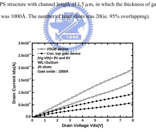
Table 3. 2 Measured optimal electrical characteristics of TFTs crystallized with VSGB-LTPS structure and conventional structure in short channel devices. The thickness of gate oxide was 1000Å. The number of laser shots was 20(ie. 95% overlapping).
Table 3. 3 Measured optimal electrical characteristics of TFTs crystallized with VSGB-LTPS structure and conventional structure in short channel devices. The thickness of gate oxide was 500Å. The number of laser shots was 10(ie. 90% overlapping).
Table 3. 4 Measured optimal electrical characteristics of TFTs crystallized with VSGB-LTPS structure and conventional structure in short channel devices. The thickness of gate oxide was 500Å. The number of laser shots was 20(ie. 95% overlapping).
Chapter 4
Table 4. 1 Measured optimal electrical characteristics of SA-VSGB-LTPS TFTs and mis-aligned VSGB-LTPS TFTs. The number of laser shots was 20(ie. 95% overlapping).
Chapter 5
Table 5. 1 Summary of the sheet resistances after CW laser and excimer laser activation. Table 5. 2 Measured optimal electrical characteristics of CLC-LTPS-TFTs and
Figure Captions
Chapter 2
Fig. 2-1 Process flow of preparing samples for material characteristics of vertical single grain boundary low temperature polycrystalline silicon thin films.
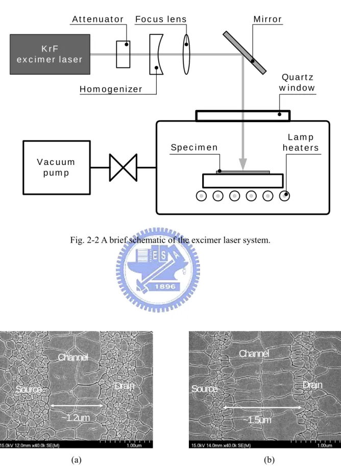
Fig. 2-2 A brief schematic of the excimer laser system.
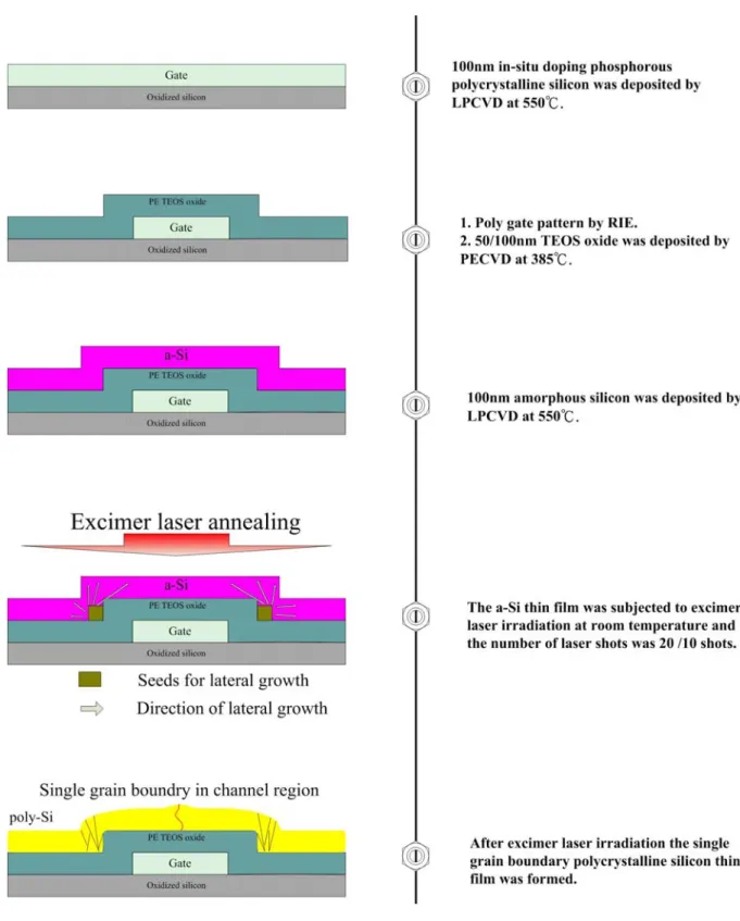
Fig. 2-3 SEM graphs of excimer laser crystallized polycrystalline silicon thin films with bottom gate structure. The channel length was 1μm (a) and 1.5μm (b). The laser energy density was 420 mJ/cm2.
Fig. 2-4 SEM graphs of excimer laser crystallized polycrystalline silicon thin films with bottom gate structure. The channel length was 2 μm. The poly gate thickness was 1000Å and the gate oxide thickness was 1000Å. The laser energy density was 420 (a) 450 (b) 480 (c).
Fig. 2-5 SEM graph of excimer laser crystallized polycrystalline silicon thin films with bottom gate structure. The channel length was 2 μm. The laser energy density was 420 mJ/cm2 and the gate oxide thickness was 1000Å. The poly gate thickness was 2000Å(a) 3000Å(b).
Fig. 2-6 SEM graphs of excimer laser crystallized polycrystalline silicon with bottom gate structure. The channel length was varied from 1.2μm to 2 μm. The poly gate thickness was 1000Å and the gate oxide thickness was 1000Å. The laser energy
density was 420 mJ/cm2
.
Fig. 2-7 Hillock formation at the grain boundaries. Driving force: density change between liquid and solid silicon. 2.53 g/cm3 for liquid silicon. 2.30 g/cm3 for solid silicon. Fig. 2-8 AFM graphs of excimer laser crystallized polycrystalline silicon thin films with
bottom gate structure. The channel length was 1.2 μm(a) 1.5μm(b). The laser energy density was 420 mJ/cm2. The poly gate thickness was 1000Å.
films with bottom gate structure. The channel length was 1.5μm. The laser energy density was 420 mJ/cm2. The poly gate thickness was 1000Å.
Fig. 2-10 Cross section TEM graph and correlated diffraction pattern of excimer laser
crystallized polycrystalline silicon thin films with bottom gate structure. The channel length was 1.5μm. The laser energy density was 420 mJ/cm2. The poly gate
thickness was 1000Å.
Chapter 3
Fig. 3-1 The key processes for fabrication of VSGB-LTPS-TFTs (I)
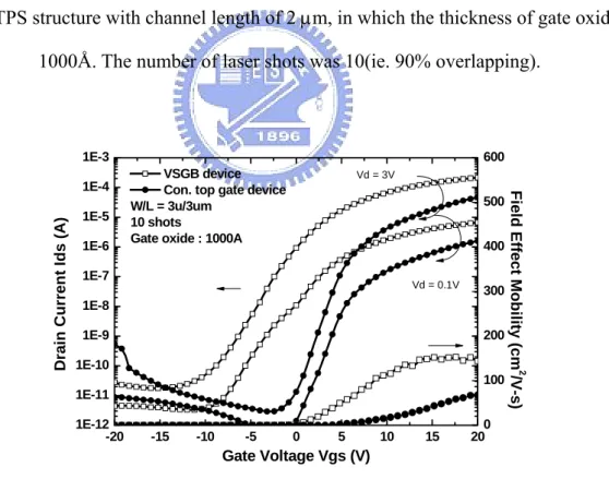
Fig. 3-2 The typical transfer characteristic of polycrystalline silicon TFTs crystallized using VSGB-LTPS structure with channel length of 1.2 μm, in which the thickness of gate oxide was 1000Å. The number of laser shots was 10(ie. 90% overlapping).
Fig. 3-3 The typical transfer characteristic of polycrystalline silicon TFTs crystallized using VSGB-LTPS structure with channel length of 1.5 μm, in which the thickness of gate oxide was 1000Å. The number of laser shots was 10(ie. 90% overlapping).
Fig. 3-4 The typical transfer characteristic of polycrystalline silicon TFTs crystallized using VSGB-LTPS structure with channel length of 2 μm, in which the thickness of gate oxide was 1000Å. The number of laser shots was 10(ie. 90% overlapping).
Fig. 3-5 The typical transfer characteristic of polycrystalline silicon TFTs crystallized using VSGB-LTPS structure with channel length of 3 μm, in which the thickness of gate oxide was 1000Å. The number of laser shots was 10(ie. 90% overlapping).
Fig. 3-6 The typical transfer characteristic of polycrystalline silicon TFTs crystallized using VSGB-LTPS structure with channel length of 5 μm, in which the thickness of gate oxide was 1000Å. The number of laser shots was 10(ie. 90% overlapping).
Fig. 3-7 The typical transfer characteristic of polycrystalline silicon TFTs crystallized using VSGB-LTPS structure with channel length of 20 μm, in which the thickness of gate oxide was 1000Å. The number of laser shots was 10(ie. 90% overlapping).
Fig. 3-8 The typical transfer characteristic of polycrystalline silicon TFTs crystallized using VSGB-LTPS structure with channel length of 40 μm, in which the thickness of gate oxide was 1000Å. The number of laser shots was 10(ie. 90% overlapping).
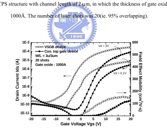
Fig. 3-9 The typical transfer characteristic of polycrystalline silicon TFTs crystallized using VSGB-LTPS structure with channel length of 1.2 μm, in which the thickness of gate oxide was 1000Å. The number of laser shots was 20(ie. 95% overlapping).
Fig. 3-10 The typical transfer characteristic of polycrystalline silicon TFTs crystallized using VSGB-LTPS structure with channel length of 1.5 μm, in which the thickness of gate oxide was 1000Å. The number of laser shots was 20(ie. 95% overlapping).
Fig. 3-11 The typical transfer characteristic of polycrystalline silicon TFTs crystallized using VSGB-LTPS structure with channel length of 2 μm, in which the thickness of gate oxide was 1000Å. The number of laser shots was 20(ie. 95% overlapping).
Fig. 3-12 The typical transfer characteristic of polycrystalline silicon TFTs crystallized using VSGB-LTPS structure with channel length of 3 μm, in which the thickness of gate oxide was 1000Å. The number of laser shots was 20(ie. 95% overlapping).
Fig. 3-13 The typical transfer characteristic of polycrystalline silicon TFTs crystallized using VSGB-LTPS structure with channel length of 5 μm, in which the thickness of gate oxide was 1000Å. The number of laser shots was 20(ie. 95% overlapping).
Fig. 3-14 The typical transfer characteristic of polycrystalline silicon TFTs crystallized using VSGB-LTPS structure with channel length of 20 μm, in which the thickness of gate oxide was 1000Å. The number of laser shots was 20(ie. 95% overlapping).
Fig. 3-15 The typical transfer characteristic of polycrystalline silicon TFTs crystallized using VSGB-LTPS structure with channel length of 40 μm, in which the thickness of gate oxide was 1000Å. The number of laser shots was 20(ie. 95% overlapping).
Fig. 3-16 The output characteristic of polycrystalline silicon TFTs crystallized using
oxide was 1000Å. The number of laser shots was 10(ie. 90% overlapping). Fig. 3-17 The output characteristic of polycrystalline silicon TFTs crystallized using
VSGB-LTPS structure with channel length of 1.5 μm, in which the thickness of gate oxide was 1000Å. The number of laser shots was 10(ie. 90% overlapping).
Fig. 3-18 The output characteristic of polycrystalline silicon TFTs crystallized using
VSGB-LTPS structure with channel length of 2 μm, in which the thickness of gate oxide was 1000Å. The number of laser shots was 10(ie. 90% overlapping).
Fig. 3-19 The output characteristic of polycrystalline silicon TFTs crystallized using
VSGB-LTPS structure with channel length of 3 μm, in which the thickness of gate oxide was 1000Å. The number of laser shots was 10(ie. 90% overlapping).
Fig. 3-20 The output characteristic of polycrystalline silicon TFTs crystallized using
VSGB-LTPS structure with channel length of 20 μm, in which the thickness of gate oxide was 1000Å. The number of laser shots was 10(ie. 90% overlapping).
Fig. 3-21 The output characteristic of polycrystalline silicon TFTs crystallized using
VSGB-LTPS structure with channel length of 20 μm, in which the thickness of gate oxide was 1000Å. The number of laser shots was 10(ie. 90% overlapping).
Fig. 3-22 The output characteristic of polycrystalline silicon TFTs crystallized using
VSGB-LTPS structure with channel length of 40 μm, in which the thickness of gate oxide was 1000Å. The number of laser shots was 10(ie. 90% overlapping).
Fig. 3-23 The output characteristic of polycrystalline silicon TFTs crystallized using
VSGB-LTPS structure with channel length of 1.2 μm, in which the thickness of gate oxide was 1000Å. The number of laser shots was 20(ie. 95% overlapping).
Fig. 3-24 The output characteristic of polycrystalline silicon TFTs crystallized using
VSGB-LTPS structure with channel length of 1.5 μm, in which the thickness of gate oxide was 1000Å. The number of laser shots was 20(ie. 95% overlapping).
VSGB-LTPS structure with channel length of 2 μm, in which the thickness of gate oxide was 1000Å. The number of laser shots was 20(ie. 95% overlapping).
Fig. 3-26 The output characteristic of polycrystalline silicon TFTs crystallized using
VSGB-LTPS structure with channel length of 3 μm, in which the thickness of gate oxide was 1000Å. The number of laser shots was 20(ie. 95% overlapping).
Fig. 3-27 The output characteristic of polycrystalline silicon TFTs crystallized using
VSGB-LTPS structure with channel length of 5 μm, in which the thickness of gate oxide was 1000Å. The number of laser shots was 20(ie. 95% overlapping).
Fig. 3-28 The output characteristic of polycrystalline silicon TFTs crystallized using
VSGB-LTPS structure with channel length of 20 μm, in which the thickness of gate oxide was 1000Å. The number of laser shots was 20(ie. 95% overlapping).
Fig. 3-29 The output characteristic of polycrystalline silicon TFTs crystallized using
VSGB-LTPS structure with channel length of 40 μm, in which the thickness of gate oxide was 1000Å. The number of laser shots was 20(ie. 95% overlapping).
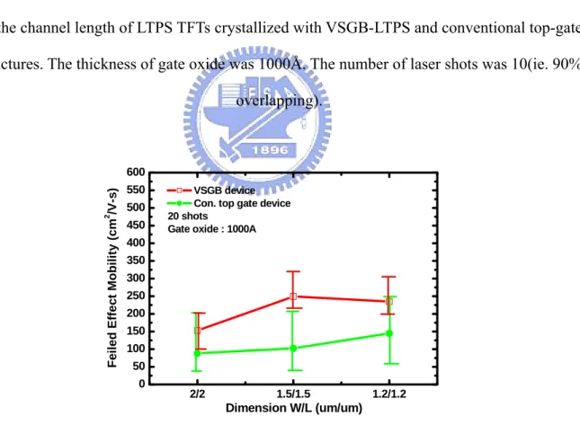
Fig. 3-30 The dependence of field-effect mobility on the channel length of LTPS TFTs
crystallized with VSGB-LTPS and conventional top-gate structures. The thickness of gate oxide was 1000Å. The number of laser shots was 10(ie. 90% overlapping). Fig. 3-31 The dependence of threshold voltage on the channel length of LTPS TFTs
crystallized with VSGB-LTPS and conventional top-gate structures. The thickness of gate oxide was 1000Å. The number of laser shots was 10(ie. 90% overlapping). Fig. 3-32 The dependences of standard deviation of field-effect mobility and threshold voltage
on the channel length of LTPS TFTs crystallized with VSGB-LTPS and conventional top-gate structures. The thickness of gate oxide was 1000Å. The number of laser shots was 10(ie. 90% overlapping).
Fig. 3-33 The dependence of field-effect mobility on the channel length of LTPS TFTs
gate oxide was 1000Å. The number of laser shots was 20(ie. 95% overlapping). Fig. 3-34 The dependence of threshold voltage on the channel length of LTPS TFTs
crystallized with VSGB-LTPS and conventional top-gate structures. The thickness of gate oxide was 1000Å. The number of laser shots was 20(ie. 95% overlapping). Fig. 3-35 The dependences of standard deviation of field-effect mobility and threshold voltage
on the channel length of LTPS TFTs crystallized with VSGB-LTPS and conventional top-gate structures. The thickness of gate oxide was 1000Å. The number of laser shots was 20(ie. 95% overlapping).
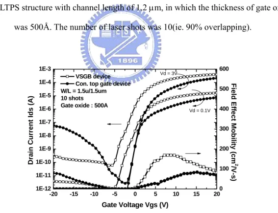
Fig. 3-36 The typical transfer characteristic of polycrystalline silicon TFTs crystallized using VSGB-LTPS structure with channel length of 1.2 μm, in which the thickness of gate oxide was 500Å. The number of laser shots was 10(ie. 90% overlapping).
Fig. 3-37 The typical transfer characteristic of polycrystalline silicon TFTs crystallized using VSGB-LTPS structure with channel length of 1.5 μm, in which the thickness of gate oxide was 500Å. The number of laser shots was 10(ie. 90% overlapping).
Fig. 3-38 The typical transfer characteristic of polycrystalline silicon TFTs crystallized using VSGB-LTPS structure with channel length of 2 μm, in which the thickness of gate oxide was 500Å. The number of laser shots was 10(ie. 90% overlapping).
Fig. 3-39 The typical transfer characteristic of polycrystalline silicon TFTs crystallized using VSGB-LTPS structure with channel length of 3 μm, in which the thickness of gate oxide was 500Å. The number of laser shots was 10(ie. 90% overlapping).
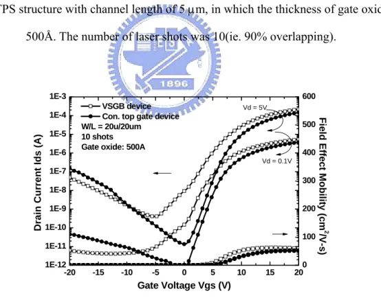
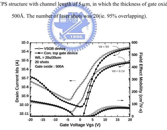
Fig. 3-40 The typical transfer characteristic of polycrystalline silicon TFTs crystallized using VSGB-LTPS structure with channel length of 5 μm, in which the thickness of gate oxide was 500Å. The number of laser shots was 10(ie. 90% overlapping).
Fig. 3-41 The typical transfer characteristic of polycrystalline silicon TFTs crystallized using VSGB-LTPS structure with channel length of 20 μm, in which the thickness of gate oxide was 500Å. The number of laser shots was 10(ie. 90% overlapping).
Fig. 3-42 The typical transfer characteristic of polycrystalline silicon TFTs crystallized using VSGB-LTPS structure with channel length of 40 μm, in which the thickness of gate oxide was 500Å. The number of laser shots was 10(ie. 90% overlapping).
Fig. 3-43 The typical transfer characteristic of polycrystalline silicon TFTs crystallized using VSGB-LTPS structure with channel length of 1.2 μm, in which the thickness of gate oxide was 500Å. The number of laser shots was 20(ie. 95% overlapping).
Fig. 3-44 The typical transfer characteristic of polycrystalline silicon TFTs crystallized using VSGB-LTPS structure with channel length of 1.5 μm, in which the thickness of gate oxide was 500Å. The number of laser shots was 20(ie. 95% overlapping).
Fig. 3-45 The typical transfer characteristic of polycrystalline silicon TFTs crystallized using VSGB-LTPS structure with channel length of 2 μm, in which the thickness of gate oxide was 500Å. The number of laser shots was 20(ie. 95% overlapping).
Fig. 3-46 The typical transfer characteristic of polycrystalline silicon TFTs crystallized using VSGB-LTPS structure with channel length of 3 μm, in which the thickness of gate oxide was 500Å. The number of laser shots was 20(ie. 95% overlapping).
Fig. 3-47 The typical transfer characteristic of polycrystalline silicon TFTs crystallized using VSGB-LTPS structure with channel length of 5 μm, in which the thickness of gate oxide was 500Å. The number of laser shots was 20(ie. 95% overlapping).
Fig. 3-48 The typical transfer characteristic of polycrystalline silicon TFTs crystallized using VSGB-LTPS structure with channel length of 20 μm, in which the thickness of gate oxide was 500Å. The number of laser shots was 20(ie. 95% overlapping).
Fig. 3-49 The typical transfer characteristic of polycrystalline silicon TFTs crystallized using VSGB-LTPS structure with channel length of 40 μm, in which the thickness of gate oxide was 500Å. The number of laser shots was 20(ie. 95% overlapping).
Fig. 3-50 Mechanism of the higher GIDL in conventional top-gate device.
VSGB-LTPS structure with channel length of 1.2 μm, in which the thickness of gate oxide was 500Å. The number of laser shots was 10(ie. 90% overlapping).
Fig. 3-52 The output characteristic of polycrystalline silicon TFTs crystallized using
VSGB-LTPS structure with channel length of 1.5 μm, in which the thickness of gate oxide was 500Å. The number of laser shots was 10(ie. 90% overlapping).
Fig. 3-53 The output characteristic of polycrystalline silicon TFTs crystallized using
VSGB-LTPS structure with channel length of 2 μm, in which the thickness of gate oxide was 500Å. The number of laser shots was 10(ie. 90% overlapping).
Fig. 3-54 The output characteristic of polycrystalline silicon TFTs crystallized using
VSGB-LTPS structure with channel length of 3 μm, in which the thickness of gate oxide was 500Å. The number of laser shots was 10(ie. 90% overlapping).
Fig. 3-55 The output characteristic of polycrystalline silicon TFTs crystallized using
VSGB-LTPS structure with channel length of 5 μm, in which the thickness of gate oxide was 500Å. The number of laser shots was 10(ie. 90% overlapping).
Fig. 3-56 The output characteristic of polycrystalline silicon TFTs crystallized using
VSGB-LTPS structure with channel length of 20 μm, in which the thickness of gate oxide was 500Å. The number of laser shots was 10(ie. 90% overlapping).
Fig. 3-57 The output characteristic of polycrystalline silicon TFTs crystallized using
VSGB-LTPS structure with channel length of 40 μm, in which the thickness of gate oxide was 500Å. The number of laser shots was 10(ie. 90% overlapping).
Fig. 3-58 The output characteristic of polycrystalline silicon TFTs crystallized using
VSGB-LTPS structure with channel length of 1.2 μm, in which the thickness of gate oxide was 500Å. The number of laser shots was 20(ie. 95% overlapping).
Fig. 3-59 The output characteristic of polycrystalline silicon TFTs crystallized using
VSGB-LTPS structure with channel length of 1.5 μm, in which the thickness of gate oxide was 500Å. The number of laser shots was 20(ie. 95% overlapping).
Fig. 3-60 The output characteristic of polycrystalline silicon TFTs crystallized using
VSGB-LTPS structure with channel length of 2 μm, in which the thickness of gate oxide was 500Å. The number of laser shots was 20(ie. 95% overlapping).
Fig. 3-61 The output characteristic of polycrystalline silicon TFTs crystallized using
VSGB-LTPS structure with channel length of 3 μm, in which the thickness of gate oxide was 500Å. The number of laser shots was 20(ie. 95% overlapping).
Fig. 3-62 The output characteristic of polycrystalline silicon TFTs crystallized using
VSGB-LTPS structure with channel length of 5 μm, in which the thickness of gate oxide was 500Å. The number of laser shots was 20(ie. 95% overlapping).
Fig. 3-63 The output characteristic of polycrystalline silicon TFTs crystallized using
VSGB-LTPS structure with channel length of 20 μm, in which the thickness of gate oxide was 500Å. The number of laser shots was 20(ie. 95% overlapping).
Fig. 3-64 The output characteristic of polycrystalline silicon TFTs crystallized using
VSGB-LTPS structure with channel length of 40 μm, in which the thickness of gate oxide was 500Å. The number of laser shots was 20(ie. 95% overlapping).
Fig. 3-65 The dependence of field-effect mobility on the channel length of LTPS TFTs
crystallized with VSGB-LTPS and conventional top-gate structures. The thickness of gate oxide was 500Å. The number of laser shots was 10(ie. 90% overlapping). Fig. 3-66 The dependence of threshold voltage on the channel length of LTPS TFTs
crystallized with VSGB-LTPS and conventional top-gate structures. The thickness of gate oxide was 500Å. The number of laser shots was 10(ie. 90% overlapping). Fig. 3-67 The dependences of standard deviation of field-effect mobility and threshold voltage
on the channel length of LTPS TFTs crystallized with VSGB-LTPS and conventional top-gate structures. The thickness of gate oxide was 500Å. The number of laser shots was 10(ie. 90% overlapping).
crystallized with VSGB-LTPS and conventional top-gate structures. The thickness of gate oxide was 500Å. The number of laser shots was 20(ie. 95% overlapping). Fig. 3-69 The dependence of threshold voltage on the channel length of LTPS TFTs
crystallized with VSGB-LTPS and conventional top-gate structures. The thickness of gate oxide was 500Å. The number of laser shots was 20(ie. 95% overlapping). Fig. 3-70 The dependences of standard deviation of field-effect mobility and threshold voltage
on the channel length of LTPS TFTs crystallized with VSGB-LTPS and conventional top-gate structures. The thickness of gate oxide was 500Å. The number of laser shots was 20(ie. 95% overlapping).
Fig. 3-71 The typical transfer characteristic of polycrystalline silicon TFTs crystallized using VSGB-LTPS TFTs structure with channel length of 1.2 μm, in which the thickness of gate oxide was 500 Å and 1000Å. The number of laser shots was 10(ie. 90% overlapping).
Fig. 3-72 The typical transfer characteristic of polycrystalline silicon TFTs crystallized using VSGB-LTPS TFTs structure with channel length of 1.5 μm, in which the thickness of gate oxide was 500 Å and 1000Å. The number of laser shots was 10(ie. 90% overlapping).
Fig. 3-73 The typical transfer characteristic of polycrystalline silicon TFTs crystallized using VSGB-LTPS TFTs structure with channel length of 1.2 μm, in which the thickness of gate oxide was 500 Å and 1000Å. The number of laser shots was 20(ie. 95% overlapping).
Fig. 3-74 The typical transfer characteristic of polycrystalline silicon TFTs crystallized using VSGB-LTPS TFTs structure with channel length of 1.5 μm, in which the thickness of gate oxide was 500 Å and 1000Å. The number of laser shots was 20(ie. 95% overlapping).
VSGB-LTPS TFTs structure with channel length of 1.2 μm, in which the thickness of gate oxide was 500 Å and 1000Å. The number of laser shots was 10(ie. 90% overlapping).
Fig. 3-76 The output characteristic of polycrystalline silicon TFTs crystallized using
VSGB-LTPS structure with channel length of 1.5 μm, in which the thickness of gate oxide was 500 Å and 1000Å. The number of laser shots was 10(ie. 90%
overlapping).
Fig. 3-77 The output characteristic of polycrystalline silicon TFTs crystallized using
VSGB-LTPS structure with channel length of 1.2 μm, in which the thickness of gate oxide was 500 Å and 1000Å. The number of laser shots was 20(ie. 95%
overlapping).
Fig. 3-78 The output characteristic of polycrystalline silicon TFTs crystallized using
VSGB-LTPS structure with channel length of 1.5 μm, in which the thickness of gate oxide was 500 Å and 1000Å. The number of laser shots was 20(ie. 95%
overlapping).
Fig. 3-79 The breakdown field of polycrystalline silicon TFTs crystallized using VSGB-LTPS structure and conventional top gate structure. The thickness of gate oxide was 1000Å.
Fig. 3-80 The breakdown field of polycrystalline silicon TFTs crystallized using VSGB-LTPS structure and conventional top gate structure. The thickness of gate oxide was 500Å. Fig. 3-81 The typical transfer characteristic of polycrystalline silicon TFTs crystallized using
VSGB-LTPS structure with channel length of 1.2 μm, in which the thickness of gate oxide was 1000Å. The number of laser shots was 10(ie. 90% overlapping). The roles of source and drain were changed for forward and reverse measurements.
Fig. 3-82 The typical transfer characteristic of polycrystalline silicon TFTs crystallized using VSGB-LTPS structure with channel length of 1.5 μm, in which the thickness of gate
oxide was 1000Å. The number of laser shots was 10(ie. 90% overlapping). The roles of source and drain were changed for forward and reverse measurements.
Fig. 3-83 The typical transfer characteristic of polycrystalline silicon TFTs crystallized using VSGB-LTPS TFTs structure with channel length of 1.2 μm, in which the thickness of gate oxide was 1000Å. The number of laser shots was 20 (ie. 95% overlapping). The roles of source and drain were changed for forward and reverse measurements. Fig. 3-84 The typical transfer characteristic of polycrystalline silicon TFTs crystallized using VSGB-LTPS structure with channel length of 1.5 μm, in which the thickness of gate oxide was 1000Å. The number of laser shots was 20 (ie. 95% overlapping). The roles of source and drain were changed for forward and reverse measurements. Fig. 3-85 The output characteristic of polycrystalline silicon TFTs crystallized using
VSGB-LTPS structure with channel length of 1.2 μm, in which the thickness of gate oxide was 1000Å. The number of laser shots was 10 (ie. 90% overlapping). The roles of source and drain were changed for forward and reverse measurements. Fig. 3-86 The output characteristic of polycrystalline silicon TFTs crystallized using
VSGB-LTPS structure with channel length of 1.5 μm, in which the thickness of gate oxide was 1000Å. The number of laser shots was 10 (ie. 90% overlapping). The roles of source and drain were changed for forward and reverse measurements. Fig. 3-87 The output characteristic of polycrystalline silicon TFTs crystallized using
VSGB-LTPS structure with channel length of 1.2 μm, in which the thickness of gate oxide was 1000Å. The number of laser shots was 20 (ie. 95% overlapping). The roles of source and drain were changed for forward and reverse measurements. Fig. 3-88 The output characteristic of polycrystalline silicon TFTs crystallized using
VSGB-LTPS structure with channel length of 1.5 μm, in which the thickness of gate oxide was 1000Å. The number of laser shots was 20 (ie. 95% overlapping). The roles of source and drain were changed for forward and reverse measurements.
Fig. 3-89 The mis-aligned ion implantation of source and drain.
Chapter 4
Fig. 4-1 The key processes for fabrication of SA-VSGB-LTPS-TFTs (I)
Fig. 4-2 OM images of self-aligned implantation devices from transparent light source. The channel length was 2μm.
Fig. 4-3 OM images of self-aligned implantation devices from transparent light source The channel length was 5μm.
Fig. 4-4 OM images of mis-aligned implantation devices after lithography. The channel length was 2μm.
Fig. 4-5 OM images of self-aligned implantation devices after lithography. The channel length was 2μm.
Fig. 4-6 SEM graphs of self-aligned implantation devices after lithography.
Fig. 4-7 The typical transfer characteristic of SA-VSGB-LTPS TFTs with amorphous gate thickness of 1000Å and 1500Å. The number of laser shots was 20 (ie. 95% overlapping).
Fig. 4-8 The output characteristic of SA-VSGB-LTPS TFTs with amorphous gate thickness of 1000Å and 1500Å. The number of laser shots was 20 (ie. 95% overlapping).
Fig. 4-9 The typical transfer characteristic of SA-VSGB-LTPS TFTs with amorphous gate thickness of 1000Å. The channel length was 1μm. The number of laser shots was 20 (ie. 95% overlapping).
Fig. 4-10 The typical transfer characteristic of SA-VSGB-LTPS TFTs with amorphous gate thickness of 1000Å. The channel length was 5μm. The number of laser shots was 20 (ie. 95% overlapping).
Fig. 4-11 The output characteristic of SA-VSGB-LTPS TFTs with amorphous gate thickness of 1000Å. The channel length was 1μm. The number of laser shots was 20 (ie. 95%
overlapping).
Fig. 4-12 The output characteristic of SA-VSGB-LTPS TFTs with amorphous gate thickness of 1000Å. The channel length was 5μm. The number of laser shots was 20 (ie. 95% overlapping).
Fig. 4-13 The typical transfer characteristic of SA-VSGB-LTPS TFTs with channel length of 1 μm, in which the thickness of gate oxide was 1000Å. The number of laser shots was 20(ie. 95% overlapping). The roles of source and drain were changed for forward and reverse measurements.
Fig. 4-14 The typical transfer characteristic of SA-VSGB-LTPS TFTs with channel length of 5 μm. The number of laser shots was 20(ie. 95% overlapping). The roles of source and drain were changed for forward and reverse measurements.
Fig. 4-15 The output characteristic of SA-VSGB-LTPS TFTs (left) and mis-aligned
VSGB-LTPS-TFTs (right) with channel length of 1 μm. The number of laser shots was 20(ie. 95% overlapping). The roles of source and drain were changed for forward and reverse measurements.
Fig. 4-16 The output characteristic of SA-VSGB-LTPS TFTs (left) and mis-aligned
VSGB-LTPS-TFTs (right) with channel length of 5 μm. The number of laser shots was 20(ie. 95% overlapping). The roles of source and drain were changed for forward and reverse measurements.
Chapter 5
Fig. 5-1 Process flows of dopant activation by CW laser annealing. Fig. 5-2 A brief schematic of the CW laser system.
Fig. 5-3 The sheet resistance after excimer laser activation. The dopant was phosphorus. The energy densities of excimer laser were varied from 190 to 390 mJ/cm2. The ion implantation doses were varied from 5X10¹⁵ to 5X1014 cm-2.
Fig. 5-5 The sheet resistance after CW laser activation. The dopant was phosphorus. The power of CW laser was 10W. The scanning rate was varied from 80mm/sec to 60mm/sec.
Fig. 5-6 The sheet resistance after CW laser activation. The dopant was boron. The power of CW laser was 10W.
Fig. 5-7 The sheet resistance after CW laser activation. The dopant was phosphorus. The power of CW laser was 15W.
Fig. 5-8 The sheet resistance after CW laser activation. The dopant was boron. The power of CW laser was 15W.
Fig. 5-9 The redistribution profiles of P31 after excimer and continuous wave laser annealings. The power of CW laser was 15W. The scanning rate was 100mm/sec. The energy density of excimer laser was 390 mJ/cm2. The number of laser shots was 20(ie. 95% overlapping). The ion implantation dose was 5X1015cm-2.
Fig. 5-10 The redistribution profiles of B11 after excimer and continuous wave laser
annealings. The power of CW laser was 15W. The scanning rate was 90mm/sec. The
energy density of excimer laser was 390 mJ/cm2. The number of laser shots was
20(ie. 95% overlapping). The ion implantation dose was 5X1015cm-2.
Fig. 5-11 Process flows of high-performance LTPS-TFTs fabricated by CW laser annealing Fig. 5-12 The typical transfer characteristics of n-type CLC-LTPS-TFTs with channel lengths
of 2μm.
Fig. 5-13 The typical transfer characteristics of n-type CLC-LTPS-TFTs with channel lengths of 5μm.
Fig. 5-14 The output characteristics of n-type CLC-LTPS-TFTs with channel lengths of 2μm. Fig. 5-15 The output characteristics of n-type CLC-LTPS-TFTs with channel lengths of 5μm. Fig. 5-16 The typical transfer characteristics of p-type CLC-LTPS-TFTs with channel lengths
Chapter 1
Introduction
1-1
Overview of Low Temperature Polycrystalline
Silicon Thin Film Transistors (LTPS TFTs)
Recently, polycrystalline silicon thin film transistors (polysilicon TFTs) were key devices in large area electronics applications, including active-matrix liquid crystal displays (AMLCDs). and active matrix organic light emitting displays (AMOLEDs) [1.1]-[1.5]. In large size active matrix liquid crystal displays (AMLCDs), the pixel switching elements were TFTs fabricated in amorphous silicon (amorphous silicon) while the peripheral driving circuitry, for which the very low amorphous silicon TFT mobility was inadequate, was fabricated on single crystal silicon. The effective carrier mobility in polycrystalline silicon was significantly higher (by two orders of magnitude) than those in amorphous silicon, so that both n- and p-channel devices with reasonably high drive currents could be achieved in polycrystalline silicon [1.6]. Therefore, the capability to realize complementary metal-oxide-semiconductor (CMOS) circuits allows low-power driving circuitry to be integrated with the active matrix [1.7]. This fact allows the integration of both the active matrix pixel switching elements and the peripheral driving circuitry onto a single glass substrate, thus substantially reducing manufacturing complexity and cost, and therefore enables the possibility of a complete system on panel (SOP) which could generate a number of innovative new products and markets. Besides, since system-on-panel mounts a screen and
its peripheral circuits on the same substrate, the successful implementation of this technology would lead to substantial savings in costs by shortening the display manufacturing and inspection processes while maintaining a level of high reliability.
One of the advantages of LTPS TFTs compared to high temperature polycrystalline silicon (HTPS) TFTs was that it could be processed at temperature low enough to utilize low cost, large area glass substrates rather than expensive quartz substrates which required process temperatures of 900°C. High-mobility polycrystalline silicon (poly-Si) thin film transistors (TFTs) fabricated in a low temperature process below 600°C were required for giant-microelectronic application. In particular, high mobility polycrystalline silicon films produced from a low temperature fabrication technique capable of utilizing an inexpensive glass substrates were thought to be fundamental to this technology. In recent years, dozens of researches have been made to develop various technologies for improving the performance and reliability of LTPS TFTs. Although polycrystalline silicon thin films could be directly deposited on glass substrate by low-pressure chemical vapor deposition (LPCVD) and electron cyclotron resonance chemical vapor deposition (ECRCVD). However, due to the high deposition temperature (approximately 625°C) and the poor crystallinity of the as-deposited polycrystalline silicon thin film, the direct deposition method has been excluded in the fabrication of LTPS TFTs. Therefore, Crystallization of amorphous silicon thin films has been considered the most important process for fabricating high-performance LTPS TFTs.
1-2
Overview for Crystallization of Amorphous
Silicon Thin Films
The crystallized polycrystalline silicon thin films always acted as channel regions in the polycrystalline silicon TFTs. Therefore, a robust crystallization process was required for LTPS
TFTs to become a mainstream technology. In order to obtain high-mobility polycrystalline silicon films, it was widely accepted that enlarging the grain size and reducing the defect density were the most important key technologies. Enlarging the grain size and reducing the defect density in polycrystalline material would make it approach the quality of single-crystalline material, which would lead to better performance of polycrystalline devices. Therefore, it was important to control the size of the grains, the number of the grains, and the location of the grains to fabricate high quality polycrystalline silicon thin films. Recently various technologies have been proposed for amorphous silicon crystallization on glass material. In several low-temperature polycrystalline silicon fabrication techniques, we could
classify them into three groups: solid phase crystallization, metal induced crystallization and
laser crystallization. In the following three kinds of low temperature crystallization methods were roughly reviewed.
1-2-1 Solid Phase Crystallization of Amorphous Silicon Thin
Films
Crystallized the as deposited amorphous silicon thin film into polycrystalline silicon have been shown to have higher carrier mobilities [1.8]. Depositing the amorphous silicon thin film at temperatures below 600°C, then thermal crystallized into polycrystalline silicon for several hours (~ 24 h) at 600°C was required to convert them into final polycrystalline form [1.9]. Unfortunately, it requires annealing for a long time(over 20 h) at high temperature (over 600°C) and therefore limits its application on large scale glass substrate for mass production requirement.
1-2-2
Metal Induced Crystallization of Amorphous Silicon Thin
Films
metals. It was well known that such method was called “metal induced crystallization (MIC)”. The reaction between the metal and amorphous silicon occurred at an interlayer by diffusion and lowered the crystallization temperature. Such enhancement of crystallization was due to an interaction of the free electrons from the metal with covalent Si bonds near the growing interface. Among various metals, Ni has been shown to be the best candidate of inducing lateral crystallization at low temperature for fabricating good-performance polycrystalline silicon TFTs. For instance, when nickel was deposited on amorphous silicon, followed by
thermal annealing, octahedral precipitates NiSi2 would be formed on amorphous silicon films
[1.10]-[1.13]. The NiSi2 precipitates act as nucleation sites for crystallization. Needlelike
crystallites were formed as a result of migration of the NiSi2 precipitates through the
amorphous silicon network. Unfortunately, the metal contamination would degrade the electrical properties such as leakage current of LTPS TFTs.
1-2-3 Laser Crystallization of Amorphous Silicon Thin Films
The laser crystallization seems to be the most promising for giant-microelectronics application. Because of its extremely short duration and shallow melt-regrowth process, this method avoids thermal damage to the glass substrate even the flexible substrate. Moreover, the polycrystalline silicon films were obtained better crystallinity by laser crystallization. The basic principle of laser crystallization was the transformation from amorphous to crystalline silicon by melting the silicon for a very short time. Laser crystallization of amorphous silicon could be performed using a variety of lasers and different techniques. Excimer laser crystallization (ELC) was by far the most widely used method at the moment [1.14][1.15]. The most important advantage of excimer lasers was the strong absorption of UV light in silicon. In consequence, most of the laser energy was absorbed close to the surface of the thin film and the thermal strain on the substrate was much lower than in case of lasers with longer wavelength. ELC of polycrystalline silicon TFTs has been studied for a number of years andseveral important aspects of this process have been well established. The technique yielded high-performance polycrystalline silicon TFTs with high throughput thanked to the large beam size of the high energy laser beam. In the recent years, substituting of the laser system was an effective way to fabricate higher mobility polycrystalline silicon channel layer. At present, the most possible laser system was continuous wave laser [1.16]. The power instability of DPSS CW laser was less than 1%, which was superior to that of KrF and XeCl excimer laser. In this technique, high scanning speed was used to achieve high throughput. The crystallized polycrystalline silicon thin film was made up of very large grains (about 3 x
20μm2). The grain boundaries were generally parallel to one another and to the scan direction
of the laser beam. However, this technique was not well-developed and the crystallization mechanisms and large-area laser annealing equipment were still under investigated.
1-3
Motivation
In order to fabricate high performance and uniform LTPS-TFTs, we introduced three methods to improve the performance and uniformity of LTPS-TFTs. In the first part, we introduced the bottom gate structure and modify the bottom gate device in various process methods. The methods were location-controlled vertical single grain-boundary (VSGB) low temperature poly silicon (LTPS) thin films transistors with bottom gate (BG) structures fabricated by excimer laser annealing and backside exposure self-aligned technology. In the grain boundary control method, we investigated a simple process to control grain growth in the channel region of TFTs. In the second part, we use novel backside exposure technology to form self-aligned VSGB-LTPS-TFTs. In the third part, we substituted the laser system by continuous wave (CW) laser to obtain LTPS-TFTs with better electrical characteristic. A novel crystallization technology of polycrystalline silicon thin film would be fabricated by
continuous wave laser.
1-3-1 Low Temperature Polycrystalline silicon (LTPS) Thin Films
Transistors with Bottom Gate (BG) Structures Fabricated by
Excimer Laser Annealing
Although conventional top-gate structure was widely used to fabricated TFTs, the high roughness between active layer and gate insulator, random grain boundary position and small process window (SLG) were noteworthy issues. Besides, there were additional process steps between active layer and gate insulator deposition which would introduce contamination in the interface between active layer and gate insulator. Therefore, we choose bottom gate structure to fabricate the high performance LTPS TFTs in the following methods.
1-3-1-1 Location-Controlled Vertical single grain-boundary (VSGB) method
Although pulsed excimer laser crystallization (ELC) had the potential to improve the crystallinity of polycrystalline silicon films, narrow ELC process window and the uniformity of the crystallized polycrystalline silicon films were important issues. According to many prior studies, the grain size of the ELC polycrystalline silicon film was significantly dependent on energy density of laser irradiation so that the energy for producing super-lateral growth was too critical to hit it right. Fluctuation of energy profile, pulse-to-pulse energy variation and unevenness of initial silicon thin films would crucially affect grain growth after solidification. As a result, many methods have been proposed to solve the above problems, such as sequential lateral solidification (SLS), phase-modulated ELC using an optical phase-shift mask, dual beam ELC, pre-pattern ELC, μ-Czochralski (so called grain filter) methods, selectively enlarging laser crystallization (SELAX) technology and etc.. However, most of them were not compatible with the existing excimer laser annealing system or needed complex processes. In this thesis, we investigate a novel ELC technique called
“Location-Controlled Vertical single grain-boundary (VSGB) method”. The objective of VSGB-LTPS-TFTs design was to fabricate thermal gradient in the selected regions. We found by experience that there was a thicker region at the corner of the bottom gate structure, i.e. the thin film containing different thicknesses at the corner region. If the laser energy density was controlled to completely melt the thin region in the channel and partially melted the thick region near the corner, a lateral temperature gradient would exist between the complete melting liquid-phase region and un-melting solid-phase seeds, and grains would grow laterally towards the center of the melting region from the un-melting solid seeds. In the first part of this thesis, the device uniformity and performance were investigated using this structure.
1-3-1-2 Self-Aligned VSGB-LTPS-TFTs Fabricated by Backside Exposure Lithography Method
Although VSGB-LTPS-TFTs exhibited superior device electrical performance and uniformity than conventional top-gate ones, one major drawback in VSGB-LTPS-TFTs was the misaligned source/drain implantation lithography owing to the non-ideal of lithography stepper system or manual alignment equipment. The mis-aligned problem would make a significant difference in turn-on characteristic of VSGB-LTPS-TFTs. Such difference would not be observed in the self-aligned case. It indicated the importance of conventional top gate device and bottom gate alignment in giving a symmetrical device as well as reducing performance variations. Therefore, many methods have been proposed to solve the above problems [1.17]-[1.19]. Among all the methods, backside exposure method seemed to be the best one to fabricate self-aligned (SA) VSGB-LTPS-TFTs on glass substrates or quartz substrates. In the second part of this thesis, we use the bottom polycrystalline silicon gate as the backside exposure mask to stop the UV lights from Hg lamp and we combined the
VSGB-LTPS-TFTs method with backside exposure technology to fabricate high performance SA-VSGB-LTPS-TFTs. The device uniformity and performance were investigated using the SA-VSGB-LTPS-TFTs configurations in ELC polycrystalline silicon TFTs.
1-3-2 Application of Continuous Wave Laser Crystallization for
Low Temperature Polycrystalline Thin Films Transistors
Substituting the laser system was an effective method to fabricate higher mobility polycrystalline silicon active layer. At present, the most potential laser system was the continuous wave (CW) laser. The power instability of DPSS CW laser was less than 1%, which was superior to that of KrF and XeCl excimer laser. In this technique, high scanning speed was used to achieve high throughput. The crystallized polycrystalline silicon thin film
was made up of very large grains (about 3 x 20μm2). The grain boundaries were generally
parallel to one another and to the scan direction of the laser beam. Surface orientation of many grains was nearly (100) direction. Surface of the crystallized polycrystalline silicon was smooth and grain boundary didn’t form ridge. CW lateral crystallization made it easy to form large grains with high scan speed and wide energy range because of continuous energy supply, directional solidification caused by laser scanning and slow cooling rate of the molten silicon thin film. In the third part of the thesis, a novel crystallization technology of polycrystalline silicon thin film would be fabricated by continuous wave laser. ELA and CW laser activation technology for phosphorus and boron dopants in amorphous silicon thin films were also performed, and taken into comparison.
1-4 Thesis Outline
In chapter 2, experimental procedures of VSGB-LTPS thin films would be introduced. The mechanisms of lateral growth of VSGB-LTPS thin films was proposed by material
analysis. The material properties of VSGB-LTPS thin films were analyzed by scanning electron microscope (SEM), atomic force microscopy (AFM) and transmission electron microscope (TEM).
In chapter 3, experimental procedures of VSGB-LTPS-TFTs would be introduced. The electrical properties of VSGB-LTPS-TFTs, including the field effect mobility, the subthreshold swing, the threshold voltage, the uniformity and bidirectional electrical properties were also investigated.
In chapter 4, VSGB-LTPS-TFTs were modified by using a novel method, so called backside exposure method. The misaligned lithography problem was observed using optical microscope (OM) and SEM. Experimental process flows would be introduced and the electrical properties of self-aligned VSGB-LTPS-TFTs, including the field effect mobility, the subthreshold swing and the threshold voltage were investigated. The bidirectional electrical properties of SA-VSGB-LTPS-TFTs was also discussed.
In chapter 5, a novel crystallization technology of polycrystalline silicon thin film was fabricated by continuous wave (CW) laser. ELA and CW laser activation technology for phosphorus and boron dopants in amorphous silicon thin films were also performed, and taken into comparison. Electrical properties of CW laser TFTs, including the field effect mobility, the subthreshold swing and the threshold voltage were also investigated.
Chapter 2
Material Analyses of Location-Controlled
Vertical Single Grain-Boundary (VSGB)
Low Temperature Poly Silicon (LTPS) Thin
Films with Bottom Gate (BG) Structures
Fabricated by Excimer Laser Annealing
(ELA)
2-1 Introduction
Currently, high driving-current capacity, low leakage-current and good uniformity of TFT characteristics over a large area of glass substrate were imperative for devices aiming at AMLCD/AMOLED drivers and matrix. Low-temperature polycrystalline silicon (LTPS) technology has been the most promising method to manufacture high performance thin film transistors (TFTs) for the past decades. As comparison to amorphous silicon (amorphous silicon), The mobility of polycrystalline silicon TFTs was generally much higher than that of amorphous silicon TFTs. The high drive current allows smaller TFTs to be used as the pixel-switching elements, resulting in higher aperture ratio. In addition, the capability to realize complementary metal-oxide-semiconductor (CMOS) circuits allowed low-power
driver circuitry to be integrated with the active matrix, for reduced display-module cost and improved reliability. As comparison to high temperature poly silicon (HTPS), the thermal budget was much lower for LTPS TFTs. The LTPS technology was compatible with glass substrate even plastic substrate. Therefore, the cost of LTPS technology was much lower than HTPS technology, especially in large panel application.
Among many techniques reported to date, excimer-laser crystallization (ELC) method seemed the most promising method for preparing high quality polycrystalline silicon thin films. The major advantage was that the polycrystalline silicon film obtained by this technology possesses good crystallinity with very few intragrain defects, due to the melt-regrowth process. But the conventional top-gate ELC LTPS TFTs have some drawbacks . First, there was higher surface roughness between active layer and insulator due to the ridge formation of grain boundaries. Second, the location of grain boundaries cannot be controlled due to the random position of nucleation during excimer laser crystallization. Third, although large grains could be obtained in the super lateral growth (SLG) regime, many small grains still spread between these large grains. According to SLG model [2.1], the lateral grain growth distance was determined by the quenching rate of liquid silicon and the retain-solid Si seed distance. Thus, a little deviation in spatial and/or pulse-to-pulse energy density and amorphous silicon thin film thickness could easily result in partial or full melting of amorphous silicon thin film at local region. Fourth, after the deposition of active layers, there were many process steps such as the pattern of active region and laser crystallization before the deposition of gate insulators. Therefore, there was possible contamination between the deposition of active layers and gate insulators.
Polycrystalline silicon thin films with large grain always resulted in high-performance polycrystalline silicon thin film devices due to the reduction of defect traps of the grain boundaries. Hence, enlarging grain size was the most effective manner for improving the
performance of the polycrystalline silicon devices. A variety of crystallization methods have been proposed to produce large grains with superior grain size distribution uniformity. They include sequential lateral solidification (SLS) [2.2]-[2.4], grain-filters (or substrate-embedded seeds) method [2.5][2.6], phase-modulated ELC using an optical phase-shift mask [2.7], ELC of selectively floating amorphous silicon thin film [2.8], ELC of pre-patterned amorphous silicon thin film [2.9]-[2.11], dual beam ELA [2.12], dual pluses ELA [2.13], slicing channel [2.14] and so on. Although all of them provided alternatives to produce large-grain polycrystalline silicon thin films, these methods could not be compatible with conventional LTPS process equipments.
It was desired that the growth of high-quality large grain could be controlled in the device channel region from the viewpoint of device performance and uniformity. In this chapter, a novel process for producing high-mobility polycrystalline silicon was described. In order to induce lateral grain growth, a lateral temperature gradient must be created between the adjacent areas and there must be retained solid Si to act as the seeds for lateral crystallization. By completely melting the amorphous Si thin film in a certain region and partially melting the one at adjacent area, a large lateral temperature gradient would exist between these two regions, and grains would grow laterally towards the complete melting region from the retained solid Si. In this method, bottom gate structures were adopted. A thick amorphous silicon region was formed in the corner due to the step structures of bottom gate which they served as the seeds for lateral grain growth during excimer laser irradiation. The laser energy density must be controlled to completely melt the thin region in the channel and partially melt the thick region near the corner. Thus, a large-grain polycrystalline silicon film was obtained which would lead to improved device performance. In addition, the lateral grain growth starting from channel edge could progress along the opposite direction toward the center of channel region. There was only one longitudinal boundary in the center of the channel. So we call this novel method, location-controlled Vertical single grain-boundary