Optimized Noise and Consistent
RF
Model
for
0.18pm MOSFETs
C. H. Huang, H. Y. Li, Albert Chin, V. Liang', and S. C. Chien'Dept. ofFlectronics Eng., National Chiao Tung Univ., Hsinchu, Taiwan United Microelectronics Coperation, Hsinchu, Taiwan
-finger 60 -+-finger 70
Abstract -Strong dependence of finger number on minimum noise figure (NFmin) is observed in O.18pm
MOSFETs. A lowest NF.;. of 0.93 dB is measured at 5.8 CHz
using 50 fingers but increases as either increasing or decreasing finger number. We have used a self-consistent S-parameter and NF,,. model to analysis this abnormal finger number dependence, and the reason is due to the combined effect of reducing gate resistance and increasing substrate loss
as increasing finger number.
I.
INTRODUCTION
By continuously scaling down the VLSI technology, the operation frequency of MOSFET-based ICs is already above GHz. Besides high operation frequency, the RF noise is another important factor for communication ICs that is directly related to S/N and limits the noise floor of a RF system. The noise source of a RF IC may come from both active MOSFET and passive device, and the major source of RF noise in passive device is from the parasitic shunt pass to ground due to the lossy Si substrate. Recently, we are able to tremendously reduce the RF noise from lossy substrate by using proton-implantation [ I]-[3] that results in record high performance transmission line [3] and antenna [4] on Si up to 20 GHz. Thus, further reducing the noise floor in a RF IC is therefore relied on the improving noise of active MOSFET. In this paper, we have used different multi-fingered layout to optimize the RF noise in 0.18pm MOSFETs. A minimum.noise figure (NFmi,J of 0.93 dB is measured at 5.8 GHz using 50 fingers, and NF,,, gradually increases as either increasing or decreasing finger number. To understand such abnormal dependence, we have used a self-consistent NF,,. and S-parameter model to simulate the MOSFET and extracted the noise source inside the equivalent circuit model. The primary noises are coming from the series gate resistance ($) and gate shunt pass to ground ($.sub & Cg.rub). The reason why a decreasing RF noise as increasing finger number <SO is due to the reduced $, while the increasing RF noise as increasing finger number >50 is due to the increased shunt
loss to substrate similar to the passive device
case
[1]-[4]. The optimized noise is therefore from the tradeoff between reducing R, and increasing shunt substrate loss that can give further device design and layout guideline for deep sub-pm MOSFETs and LNAs.11.
EXPERIMENTAL PROCEDURE
Multi-fingered layout of 0.18pm MOSFETs are used in this study. To achieve a low gate resistance, a silicide gate technology is applied. The finger width is 5 pn and the finger number is ranged from 20 to 70 at an increment of IO. The multi-fingered structure with a small finger width
enables us to reduce both the DC silicide gate resistance and the RF non-quasi-static gate resistance [5]. The devices are first characterized by DC I-V and reliability test [6]. Then standard 2-port S-parameters are measured using HP8510B network analyzer and on-wafer probes and de-embedded from the probe pad. The NF,, and associate gain are measured using standard ATN-NP5B Noise Parameter Extraction System up to 7.2 GHz that covers the most important frequency range for wireless communication. Numerical simulation was performed by using an equivalent circuit model of intrinsic MOSFET with additional terminal resistance and shunt pass to ground at both input and output ports [7]. To avoid non-physically based data in the equivalent circuit model, DC and low frequency data are measured and referred in circuit model.
111.
RESULTS
AND
DISCUSSION
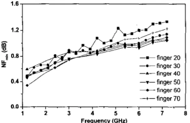
A . Measured NF,, andfinger dependence.Fig. 1 shows the measured NF,,, as a function of frequency and finger numbers. A general trend of increasing noise is observed for all the multi-fingered MOSFETs as increasing frequency, and a small NF,,, ranged from 0.5 to 1.5 dB is measured over the measured frequency range that indicates the good noise performance. However, the measured NF,,, is strongly dependent on the number of fingers.
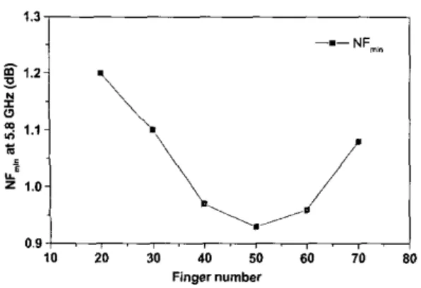
To further investigate such gate finger dependence, we have plotted the NF,, as a function of finger number at a frequency of 5.8 GHz used for wireless local-area network (LAN). As shown in Fig. 2, an abnormal dependence of NF,,, on finger number is observed: the NF,,. first decreases as increasing gate finger until a smallest NF,,. of 0.93 dB is measured at a finger number of SO and then the
NF,,, increases as increasing finger number above 50.
0-7803-7765-6/03/$17.00 0 2 0 0 3 IEEE.
1.3
-.-
NFm," Y.i
1
z 1.0\
/
I
10 20 30 40 50 60 70 80 Finger numberFig. 2. Finger number dependence on NF,,, of 0.18pm MOSFETs at 5.8 GHz. The lowest NF,, of 0.93 dB is obtained at a finger number of 50.
B. Modeled NF,, and S-parameters.
We have used the equivalent circuit model [7] to analyze such abnormal gate finger dependence on NF,,,. Fig. 3 shows the equivalent circuit model used for multi-fingered 0.18pm MOSFETs. The same model is used for all the gate finger numbers from 20 to 70, but each value of the circuit elements is dependent on the different finger numbers. This model also provides a self-consistent simulation between NF,,, and S-parameters that can be further used to investigate the dominated noise source in 0.1 @m MOSFETs.
Poit2
Fig. 3. Thc equivalent circuit model of multi-fingered 0.18pm MOSFETs.
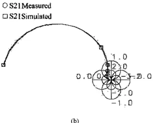
Figs. 4(a) and 4(b) present the measured and modeled S-parameters plotted at radius of I and 6 respectively, with the smallest finger number of 20. Figs. 5(a) and 5(b) show the measured and modeled S-parameters plotted at radius of I and I1 respectively, with the largest finger number of 70. Good agreements between measured and modeled data arc obtained for finger number of 20 and 70. Although the S-parameters for gate fingcr from 30 to 60 are not shown, similar good agreement between measured and modeled S-parameters are also achieved. The excellent agreement between measured and modeled S-parameters suggests the good accuracy of our equivalent circuit model. 1.0 Measured 0 (4
0
S2
I Measured
0
S2
1Simulated
2 . 0 (h)Fig. 4. The simulated and measured S-parameters of 0 . 1 8 ~ m MOSFETs plotted in respective radius of (a) I and (h) 6, and the finger number is 20.
Measured 1.0
0
Fig. 5(a) Thc simulated and measured S-parameters af 70 fingered 0. I 8 p MOSFETs plotted in respective radius of 1
0
S2
1Measured
0S2
I Simulated
1.8 1.6- 1.4--
1.2- m 3 . 1.0- E ._y
0.8- 0.6- 0.4: (b)Fig. 5(b) The simulated and measured S-parameters of 70 fingered 0 . I S p MOSFETs plotted in respective radius of 11.
We have further examined the measured and equivalent circuit modeled NF,, among various gate fingers. Figs. 6 and 7 show the measured and modeled NF,, for the finger number of 20 and 70, respectively. Good agreement between measured and modeled NF,, is achieved for these two gate fingers over the entire measured frequency. Similar good agreement between measured and modeled NF- are also obtained for gate fingers from 30 to 60 (not shown). It is noticed that both S-parameters and NF,, are generated at the same model for a specific gate finger without changing any value of equivalent circuit elements. The good agreement between measured and modeled S-parameters and NF,, indicate the excellent accuracy of this equivalent circuit model.
.finger number20
.,-
.-.-.
,..’
,.I.,-:,.
-e- measured._.’
.’ .,”
0 . 2 , , , ,,
. , , , , Frequency (GHz)Fig. 6 . The simulated and measured NF,,, as a function of frequency of multi-fingered 0 . 1 8 p MOSFET with a finger number of 20.
C. Origin of abnormal NF,;, dependence onfinger number:
After achieving good agreement between measured and modeled S-parameters and NF,, among different fingers, we have further compared the equivalent circuit elements and the results are summarized in Table 1. Because the noise of a cascade system follows the well known equation,
1.4 finger number 70 ,d. 1.2
*
,
,
<
:
.
,
.‘-
-*-measuredI
Frequency (GHr) 0.2 , , . , , , . ,. L ,
, , . 1 2 3 4 5 6 7 8Fig. 7 . The simulated and measured NF,, as a function of frequency for multi-fingered 0.18pm MOSFET with a finger number of 70.
(1)
F2 -1
FN
- 1F = & + -
+
...
+
GI
G , G ,
...
GN.)the noise in the MOSFET is dominated by gate input terminal before amplified to drain output terminal. However, the influence of drain terminal becomes important at large gate fingers because of the increasing reverse feedback that is not considered in equation (1). Therefore, the thermal noise from R, is the primary noise source in the MOSFET. This also explains the reduced NF,,, as increasing gate fingers less than 50. It is noticed that a relatively large R, listed in Table 1 may he due to the non-quasi-static effect. The reason why increasing NS,,, as increasing gate fingers above 50 is due t o the increasing shunt substrate loss to ground as evidenced from the decreasing Rgiub and increasing Cg.sub in Table I. From above discussion, further scaling down the gate length beyond 0.18pm will be probably unable t o further reduce the RF noise, because of the increasing
4
by a smaller gate area, the existing same shunt substrate loss as 0.18pm case, and the increasing reverse feedback from output terminal (short channel effect).IV. CONCLUSION
We have measured and modeled the NF,. and S-parameters o f multi-fingered 0.18pm MOSFETs. Strong dependence of NF,,, on layout finger number is found that
is
dueto
thecombined
effect of&
and
shuntpass
to substrate. A very small NF,,, of 0.93 d B is measured for a finger number of 50 at 5.8 GHr that indicates the good potential application for high performance LNA for wireless LANs.ACKNOWLEDGEMENT
The authors would like to thank Dr. K. M. Chen, Mr. Y. M. Deng and Dr. G. W. Huang at National Nano Device Lab. (NDL) for their help in the measurement. This work has been supported by NSC (90-2215-E-009.052) and UMC.
Table 1.
Important device parameters used for multi-fingered 0. I8pm MOSFETs.
REFERENCES
[ I ] Y. H. Wu, A. Chin, K. H. Shih, C. C. Wu, S. C. Pai, C. C. Chi, and C. P. Liao, “RF loss and cross talk on extremely high resistivity (10K-IM-cm) Si fabricated by ion implantation,” IEEE MTT-S Int. Microwwe Symp. Dig., pp. 241-244, June 2000
[2] Y. H. Wu, A. Chin, K. H. Shih, C. C. Wu, C. P. Liao, S. C. Pai, C. C. Chi, “The fabrication of very high resistivity Si with low loss and cross talk,” IEEE Electron Device Lett. 21, pp. 394-396,2000,
[3] K. T. Chan, A. Chin, C. M. Kwei, D. T. Shien, and W. J. Lin, “Transmission line Noise from Standard and Proton-Implanted Si,” IEEE MTT-S Inl. Microwave Symp. Dig., June 2001.
[4] K. T. Chan, A. Chin, Y. B. Chen, Y-D. Lin, D. T. S. Duh, and W. J. Lin, “Integrated antennas on Si, proton-implanted Si and Si-on-Quartz,” 1x1. Electron Devices Meeting IEDM Tech. Dig., Dec. 2001, Washington DC, USA.
[5] X. Jin, J. J. Ou, C. H. Chen, W. Liu, M. J. Deen, P. R. Gray, and C. Hu, “An effective gate resistance model for CMOS RF and noise modeling,” Int. Electron Devices Meeting IEDMTech. Dig., pp. 961-964. 1998.
[6] A. Chin, C. S. Liang, C. Y Lin, C. C. Wu, and J. Liu, “Strong and efficient light emission in ITO/AI,O, superlattice tunnel diode,” Int Electron Devices Meeting IEDMTech. Dig., Dec. 2001, Washington DC, USA.
Y. H. Wu, A. Chin, C. S. Liang, and C. C. Wu, “The performance limiting factors as RF MOSFETs scaling down,”Int. RF-ICSymp., pp. 151-155, June 2000.
[7]