TU4B-5
The minimum noise figure and mechanism as scaling RF MOSFETs
from 0.18 to 0.13
ym
technology nodes
C. H.
Huangl,
K. T. Chanl, C. Y.
Chenl,
Albert Chin', G. W. Huang', C. Tseng',
V.
Liang',
J. K.
Chen'and S. C. Chien3
Dept.
of
ElectronicsEng.,
N a t i o n a lChiao Tung Univ., Hsinchu, Taiwan
National Nano Device Lab, Hsinchu, Taiwan
U n i t e d Microelectronics
Cooperation, Hsinchu,
Taiwan
I2 3
Abstract - As scaling down the KF MOSFET from 0.18 to of
RF
technology on high conductivity Si substrates [3]-[610.13 pm technology nodes, the fr increases but the NFm. and is especially important for passive transmission lines becomes worse by increasing -4.2- dB. A small NE.,. of 0.93 and inductom.
ne
down .dB is measured at 5.8 GHz in 0.18w
MOSFET using 50kom 0 . ~ 8 to 0.13 due to the number. This abnormal dependence and higher at increased Rg-nqI because of the smaller gate area and larger
0 . 1 3 ~ ~ is analyzed by model resistance as scaling down. Therefore, the scaling below and due to the combined gate resistance and substrate efiect. 0.13 pm technology node may further degrade the
RF
increasing NF,;. as
technology node is fingers but increases as either increasing er decreasing finger
noise unless a modified T-gate structure is used. 1. INTRODUCTION
The performance improvement and circuit area reduction are the driving force for continuously scaling down the MOSFET into RF frequency regime [1]-[2]. However, it is not clear if the RF noise can also be Continuously improved as scaling down the MOSFET [I]. Next, the dominant noise sources in RF MOSFET are still
not quite understood and the optimized device layout for achieving minimum noise figure (NF,;.) is also unclear. In
this paper, we have studied the
RF
MOSFETs scaled from 0.18 to 0.13 pm technology nodes. The scaling gives better RF power gain and fr. However, we have found that the scaling did not give better NF,,, but increasing by -0.2 dB at the same gate width. We have used the'well calibrated equivalent circuit model to analyze such abnormal effect and the multi-fingered layout to optimize the NF,;.. The NF,, decreases with increasing gate finger to a small value of 0.93 dB at 5.8 GHz using 50 fingers layout in 0.18 pm MOSFETs. Similar decreasing NF,i. with increasing gate finger is also found uisng 0.13 pmtechnology node. However, we have measured another abnormal increase of NFmm when increasing gate finger >50 in 0.18 pm device. From our equivalent circuit model analysis, the decreasing NF,,. with increasing gate finger is due to the decreasing thermal noise generated by non- quasi-static gate resistance (R& [2] that is due to the delayed tun-on in gate electrode. The thermal noise generated by F& is also the primary noise source in RF
MOSFETs. The abnormal NF,,. increase at
>SO
fingers is due to the increasing parasitic shunt RC pass to substrate and modeled by Zg.,ub, This is the fundamental limitation11. EXPERIMENTAL PROCEDURE The RF MOSFETs using 0.18 and 0.13 pm technology nodes are studied in this work. In additional to the low resistance silicide gate technology, the multi-fingered gate layout can further reduce the gate resistance by connecting in parallel. The finger width is 5
w
and the finger number is ranged from 20 to 70 at an increment of IO. The devices are characterized by DC I-V and 2-port S- parameters using HP8510C network analyzer from 300 MHz to 30 GHz. Then regular de-embedding procedure is followed to eliminate the parasitic effect of probe pad. The NF,,, and associate gain are measured using standard ATN-NPSB Noise Parameter Extraction System up to 7.2 GHz that covers the most important frequency range for wireless communication. The extraction of dominateRF
noise sources were performed by using an equivalent circuit model of intrinsic MOSFET with additional terminal resistance and shunt pass to ground at both input and output ports. To avoid non-physically based data in the equivalent circuit model, DC and low frequency data are measured and referred in circuit model.
111. RESULTS AND DISCUSSION A. Measured NF,, in
RF
MOSFETs usedfor circuil:Fig. 1 shows the circuit schematic of a typical two-stage low noise amplifier (LNA) [7]. From the RF circuit theory, the noise of the whole LNA is determined by the MOSFET in the first stage. Therefore, the choosing
0-7803-7694-3/03/$17.00 0 2003 IEEE
313
proper MOSFET to have a lowest NF,;.
is
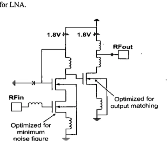
the key factor for LNA.1.8V
RFin Optimized for
output matching Optimized for
minim U m
noisefigure =
Fig. I , The schematic of a two Stage LNA. The MOSFET at first stage determines the minimum noise in LNA.
Fig. 2 shows the measured NF,,. for
RF
MOSFETs at0.18 and 0.13 pn technology nodes. The measured NF,,.
shows a general trend of decreasing
RF
noise with increasing the gate finger for MOSFETs in both technology nodes. A small NF- of 0.93 dB is measured at 5.8 GHz using 50 gate fingers in 0.18 pm case, which shows the excellent noise performance at such high frequency and can be used for wireless LAN application. However, the NF,;. increases by -0.2 dB as scaling down from 0.18 to0.13
pn technology node, which is opposite to the scaling trend. In addition, an abnormal increase of NF,,. is observed as gate fingers increasing >50 in 0.18pm case.
1.8
Solid: measured NF_-
I
Y 'a0.61
z
0.3
-
-
0 . l S p technology node MOSFETs0.13pm technology node MOSFETs
0 . 0 ' . I , I . 8 . I , I ' I
10 20 30 40 50 60 70 80 Fig. 2. The measured NF,;. of RF MOSFETs at 0.18 and 0.13 pm technology nodes. The scaling from 0.18 to 0.13 pm technology gives a worse NF,,.. An abnormal increase of NF,;. at gate finger > SO is also observed in 0.18pm case. The
modeled data is from the equivalent circuit model in Fig. 7.
Finger number
It is noticed that the measured
NF,;.
of MOSFET at 0.13 pm node is comparable with the data published in the literature by IBM [I]. Therefore, the increasing NF,,, in 0.13 pm case may be intrinsic to device physics rather than the different technology among different companies.Fig. 3 shows the associated gain measured at 5.8 GHz under NF,;. condition. A decreasing trend of associated gain with increasing gate finger is measured for both MOSFETs using 0.18 and 0.13 pm technology nodes. Therefore, the decreasing RF noise in Fig. 1 is traded
o f f
by the decreasing associated gain. The reason why such decreasing associated gain is explained by following relation derived from equivalent model [Z]:
Although the decreasing
RF
noise is achieved by decreasing Rgqi using parallel gate fingers, the increasing finger number also increases the undesired Cad that decreases the associated gain."i7",
, , , , ,,
,,
,1
i
-0.13pm10 20 30 40 50 60 70 80
$ 0
Finger number
Fig. 3. The associated gain measured at 5.8 GHz under NF,. condition for RF MOSFETs at 0.18 and 0.13 pm technology
nodes. The scaling from 0.18 to 0.13 pm gives higher associated
gain but increasing finger number decreases the associated gain. The increasing gate finger for achieving lower RF noise is also trades off the decreasing fr. Fig. 4 shows the fr of MOSFETs using 0.18 and 0.13 pm technology nodes. The scaling from 0.18 to 0.13 pm technology improves the fr
to -100 GHz that shows the good device performance. It
is noticed that the fi decreases as increasing the number of gate fingers, which can be understood by following relation [Z]:
f,=
(2)
6% 1
The increasing finger number improves the RF noise but also increases the parallel Cgd that decreases the fr.
901
\
""1
'z
..3
-0.18um -r, ""-
0.13pm 20 r .. 70--
.
, . , . '10 20 30 40 50 60 Finger number1
80Fig. 4. The finger number dependent fT of RF MOSFETs using
0.18 and 0.13 pm technology nodes. The increasing finger number decreases the fr.
The large gate fmger number layout in RF MOSFET not only achieves a lower RF noise but also has better output matching. Fig. 5 shows the S I 2 of MOSFETs at
0.13 Mm nodes. The increasing gate finger shifts the
measured S2? and pushes the output resistance of
MOSFET (by extending the S22 to low frequency) close to
50 R. This is important to choose the proper transistor layout at second stage of LNA shown in Fig. 1.
I
Fig. 5. The measured S22 of RF MOSFETs in 0.13 ~m nodes. The increasing finger number shifts the output resistance of S2> and close to the desired 50 R.
B. NF,, analysis using self-consisrent model of S-
parameter & NF,,:
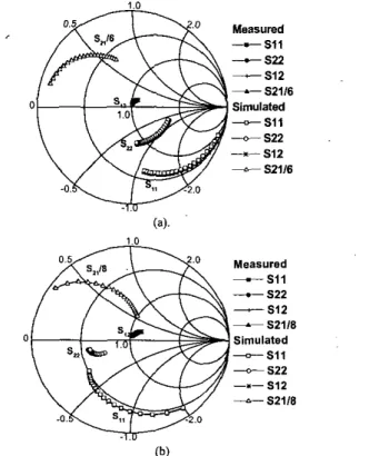
To further analyze the RF noise, we have developed a self-consistent model for both S-parameter and 'NFmi.. Figs. 6(a) and 6(b) show the measured and modeled S-
parameters using the model shown in Fig. 7. Good matching between measured and modeled S-parameten and DC I-V (not shown) are obtained for RF MOSFETs in
0.13 pn nodes with the smallest 20 and largest 70 gate
fingers. The good agreement between measured and modeled data is also obtained in other gate fingers of MOSFETs using both 0.13 and 0.18 pm technologies.
1.0 Measured -s11
-
S i 2-
S I 2-
52116 0 Simulated - S l l-
522-
-
S I 2 S2116 1.0 Measured - s i 1-
s22 - s i 2-
52118 Simulated - S I 1-
522-.-
SI2-
52'118 (b)Fig. 6. ?he measured and simulated S-parameters of RF MOSFETs with (a) the smallest 20 fingers and (b) largest 70
fingers using 0.13 pm technology node. The SI, in (a) and @) is divided by 6 and 8 respectively, to fit in the Smith chart.
Bsim3v3 intrisic mcdel
Fig. 7. The self-consistent model far DC I-V, S-parameters and
NF,,..
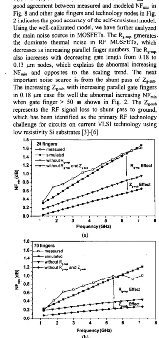
Using the samt ,.Loodel, we have further simulated the NF,j. self-consistently with SLparameter and DC 1-V. Figs. 8(a) and 8@) show the measured and modeled NF,;.. The good agreement between measured and modeled NFmj. in
Fig.
8
and other gate fingers and technology nodes in Fig. 2 indicates the good accuracy of the self-consistent model, Using the well-calibrated model, we have further analyzed the main noise source in MOSFETs. The $.mqs generates.the dominate thermal noise in RF MOSFETs, which decreases as increasing parallel finger numbers. The $.nqs
also increases with decreasing gate length from 0.18 to
0.13 pm nodes, which explains the abnormal increasing
. NF,, and opposites to the scaling bend. The next important noise source is from the shunt pass of ZeEUb. The increasing Z,.,.a with increasing parallel gate fingers
in 0. I8 pm case fits well the abnormal increasing NF,, when gate finger > 50 as shown
in
Fig. 2. The Z,,,represents the
RF
signal loss to shunt pass to ground, which has been identified as the primary RF technology challenge for circuitson
current VLSl technology using low resistivity Si substrates[ 3 ] - [ 6 ] .
Frequency (GHz) (a) z R, Eif& 0.6 0.4 0.2 0.0 1 2 3 4 5 6 7 8 Frequency (GW) (b)
Fig. 8. The measured andsimulated NF,,. of RF MOSFETs with
(a) the smallest 20 fingers and (b) largest 70 fingers using 0.13 pm technology. Good agreement is obtained for all other gate fingers and also for 0.18 pm case
IV. CONCLUSIONS
The abnormal
NF,;.
increases as scaling the MOSFET from0.18
to0.13
pm nodes has been identified by the increasing $..qv The abnormal increasing NF,,. of 0.18pm MOSFETs at gate finger > 50 is modeled by the increasing shunt pass loss to ground. Unless a T-gate MOSFET structure is used similar to 111-V RF FET, the increasing gate resistance with continuous scaling is the fundamental limitation of
RF
noise in MOSFETs.ACKNOWLEDGEMENT
We would like to thank D. C. Nio at National Chung- Chen Science Research Inst. This work has been supported by NSC (90-2215-E-009-044).
REFERENCES
[I] N.’Zamdmer, A. Ray, JLO. Plouchart, L. Wagner, N. Fang, K. A. Jenkins, W. Jin, P. Smeys, 1. Yang, G Shahidi, and F. Assaderaghi, “A 0.13-pm SO1 CMOS technology for low- power digital and RF applications,” VLSI Tech. Symp. Dig.,
pp. 85-86, June 2001.
[2] Y . H. Wu, A. Chin, C. S. Liang, and C. C. Wu, “The performance limiting factors as RF MOSFETs scaling down,” IEEE W - I C Internolionoi Microwove Symp. Dig.,
pp. 151-154, June 2000.
[3] K. T. Chan, A. Chin, C. M. Kwei, D. T. Shien, and W. J. Lin, “Transmission line Noise from Standard and Proton- Implanted Si,” IEEE ~ - S l n t e r n a t i o n o l Micmwove S y ” . Dig., pp. 763-766, June 2001.
[4] Y. H. Wu, A. Chin, K. H. Shih, C. C. Wu, S. C. Pai, C. C. Chi, and C. P. Liao, “RF loss and cross talk an exeemely high resistivity (IOK-IMR-cm) Si fabricated by ion implantation,” IEEE MTT-S International Miemwove Symp. Dig., pp. 221-224, June 2000.
[5] K.
T,
Chan, A. Chin, Y. B. Chan, T. S. Duh and W. I. Lin, “Integrated antenna on Si, proton-implanted Si and Si-on- Quartz,’’ Intemotionoi Eleclmn Devices Meeting VEDM) Tech. Dig.. pp. 903-906, Dec. 2001.[6] K. T. Chan, C. Y. Chen, A. Chin, I. C. Hsieh, I. Liu, T. S. Duh, and W. 1. Lin, “40-GHz Coplanar Waveguide Bandpass Filters an Silicon Substrate,” IEEE wireless &
Microwove Components Lett 23, no. I I, pp. 429431,2002. 171 U. K. Shaeffer and T. H. Lee, “A 1 . W 1.5 GHz CMOS Law Noise Amplifier,” Symp on VLSl Circuit Dig., p p . 32-
33, June 1996.