Hole mobility enhancement of Si
0.2Ge
0.8quantum well channel on Si
C.-Y. Peng, F. Yuan, C.-Y. Yu, and P.-S. KuoDepartment of Electrical Engineering, National Taiwan University, Taipei, Taiwan 106, Republic of China and Graduate Institute of Electronics Engineering, National Taiwan University, Taipei, Taiwan 106, Republic of China
M. H. Lee
Institute of Electro-optical Science and Technology, National Taiwan Normal University, Taipei, Taiwan 106, Republic of China
S. Maikap
Department of Electronics Engineering, , Chang Gung University, Kwei-Shan, Tao-Yuan, Taiwan 333, Republic of China
C.-H. Hsu
National Synchrotron Radiation Research Center, Hsinchu, Taiwan 30076, Republic of China C. W. Liua兲
Department of Electrical Engineering, National Taiwan University, Taipei, Taiwan 106, Republic of China, Graduate Institute of Electronics Engineering, National Taiwan University, Taipei, Taiwan 106,
Republic of China and National Nano Device Laboratories, Hsinchu, Taiwan 30076, Republic of China 共Received 27 July 2006; accepted 23 October 2006; published online 4 January 2007兲
The ultrathin strained Si0.2Ge0.8quantum well channel共⬃5 nm兲 directly grown on Si substrates is demonstrated with low defect density and high hole mobility. The quantum well Si0.2Ge0.8channel reveals an ⬃3.2 times hole current enhancement and an ⬃3 times hole mobility enhancement as compared with the bulk Si channel. The output current-voltage characteristics under the external mechanical strain confirm the compressive strain in the channel. The external compressive strain further enhances the hole mobility in a Si0.2Ge0.8channel. © 2007 American Institute of Physics. 关DOI:10.1063/1.2400394兴
The superior transport property of Ge has high electron and hole mobilities and can reach the high performance tar-get in the future Si technology. However, the cost and insuf-ficient abundance of Ge in the Earth make it difficult to replace Si. The dual channel共strained Si and strained Ge兲1 and the Ge channel2 on relaxed SiGe buffer structures have significant mobility enhancements but suffer the disadvan-tages of threading dislocation defect, rough surface, and high cost of SiGe virtual substrate. The ultrathin SiGe epitaxially grown directly on Si with compressive strain has the advan-tages of high mobility, low cost, and the compatibility with Si process. In the previous work, the hole mobility enhance-ments of ten times,1six times,2two times,3and three times4 have been reported, and all are based on thick Ge layers 共⬃400 nm兲 or SiGe buffers 共1–2m兲. In this letter, we in-vestigate the ultrathin SiGe channel of a p-channel field ef-fect transistor共PFET兲 with the Schottky barrier source and drain.
The epi-Ge layer 共⬃5 nm兲 was grown on a Si 共100兲 substrate at 525 ° C by ultrahigh-vacuum chemical vapor deposition. However, the fast diffusion of Si into Ge共Ref.5兲
forms the Si0.2Ge0.8layer at the final stage of the growth. To improve the interface between the gate insulator and the Si0.2Ge0.8/ Si channel, a nominal ⬃3 nm Si cap layer is
grown on the top of epi-Ge layer to passivate and smoothen the surface. Due to the slow diffusion of Ge into Si, the cap composition is dominated by Si. The roughnesses of nominal 3 and 1 nm Si caps on the Si0.2Ge0.8 channel are 0.5 and
0.62 nm, respectively, measured by atomic force microscope on the area of 10⫻10m2. Tacking the process into
consid-eration, the thin cap共1 nm兲 was completely oxidized due to the exposure to the air in the fabrication, and the inferior Ge oxide existed at oxide/Si0.2Ge0.8interface with a large
inter-face density of 1.5⫻1012 cm−2eV−1 as compared to 2
⫻1011cm−2eV−1for an initial 3 nm cap. The Si cap in our
device is a sacrificial and passivation layer for the SiGe channel, and its thickness is reduced after the device fabri-cation. However, if the Si cap can be maintained after the process, the thinner remaining Si cap can have a higher chan-nel mobility.6As a result, the nominal⬃3 nm Si cap layer is essential for our device and approximately 1 nm Si cap layer remains after processing. The gate stack consists of ⬃300 nm tetra-ethyl-oxy-silane 共TEOS兲 gate dielectric and a polygate with P implantation activated by rapid thermal
an-a兲Author to whom correspondence should be addressed; electronic mail:
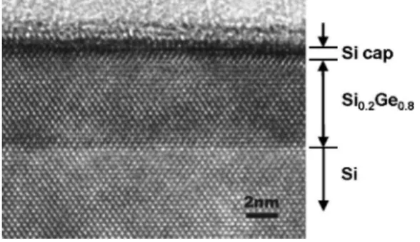
FIG. 1. TEM image of a Si0.2Ge0.8 quantum well on Si with a nominal
⬃3 nm Si cap layer. Due to consumption of the Si cap in the process, only an⬃1 nm cap layer was observed by TEM.
APPLIED PHYSICS LETTERS 90, 012114共2007兲
0003-6951/2007/90共1兲/012114/3/$23.00 90, 012114-1 © 2007 American Institute of Physics
nealing 共650 °C, 10 s兲. The one-mask process was used to fabricate PFET,7 and Pt was used as the Schottky barrier source and drain.8
The transmission electron microscope image of the Si0.2Ge0.8layer with a nominal⬃3 nm Si cap layer is shown
in Fig.1. Due to the consumption of the Si cap in the pro-cess, only an⬃1 nm cap layer was observed. It shows no apparent defect or dislocation in the image. The 5 nm SiGe layer is too thin for the regular x-ray diffraction共XRD兲. The high intensity source was available in the synchrotron radia-tion and was used to probe the lateral lattice constant using the H scan 共in-plane XRD兲. The 5 nm SiGe layer revealed the same lateral lattice constant as the Si substrate, and the Ge concentration estimated by Raman shift is about 80%. Figure 2 shows that the hole concentration of a Si0.2Ge0.8
quantum well at inversion bias is mainly located in the Si0.2Ge0.8quantum well by the simulation with a 1 nm Si cap and a 5 nm Si0.2Ge0.8 well. The ⬃5 nm Si0.2Ge0.8 layer is
sufficient for the hole conduction channel.
The 5 nm HfO2 are deposited on the Si/ Si0.2Ge0.8/ Si
quantum well to measure the capacitance-voltage 共C-V兲 characteristics. The results show that the equivalent oxide thickness is 2.5 nm and the leakage current is 7.3⫻10−5A / cm2at 1 V. Figure3 shows a shoulder on the
C-V curve measured at 100 Hz, indicating the hole con-finement in the Si0.2Ge0.8 quantum well. The existence of
this shoulder at different measurement temperatures
共−100–30 °C兲 suggests that it should not be originated from defects.9 To observe the confinement shoulder in the C-V curve, the dielectric thickness should be comparable to the Si0.2Ge0.8thickness, thus the thin HfO2is used. The centroid
of hole concentration 共inset of Fig. 3兲 extracted from the
C-V plot10 is 2.2 nm from the surface, which is consistent with the simulation result共Fig.2兲.
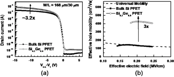
The transfer characteristics measured at the drain bias= −0.1 V for a Si0.2Ge0.8quantum well device and a con-trol Si device are shown in Fig. 4共a兲. The Ion/ Ioff ratio is
4⫻106 for the Si
0.2Ge0.8 device. The leakage current
domi-nated by electron is still larger than that of the bulk Si device due to the lower barrier height共Bn= 0.78 eV兲 for electron
injection in the off state than bulk Si device共Bn= 0.85 eV兲.
The Si0.2Ge0.8PFET shows an⬃3.2 times drain current
en-hancement in the saturation region 关Fig. 4共a兲兴. Due to the thick TEOS gate oxide needed for the one-mask process, the estimated ideal VT for the control Si device is −5.4 V. The
deviation between the ideal VT and the experimental value
共−8.3 V兲 may come from the fixed oxide charges and the interface trapped charges. The Si0.2Ge0.8 PFET has a
rela-tively smaller magnitude of VT 共−7.4 V兲 than that of the
control Si device共−8.3 V兲 due to the hole confinement in the SiGe quantum well. Figure 4共b兲 shows the hole mobility measured by the split C-V technique. The approximately FIG. 2. Hole concentration for the Si0.2Ge0.8quantum well device and the
bulk Si device by quantum mechanical simulation. The hole concentration of the Si0.2Ge0.8quantum well device is higher than that of bulk Si device due to the hole confinement in the Si0.2Ge0.8quantum well channel.
FIG. 3. C-V characteristics of Si0.2Ge0.8 quantum well
metal-oxide-semiconductor capacitor on a n-type Si substrate with a Pt/ TaN metal gate and a 5 nm HfO2insulator. The confinement shoulder in the C-V plot indi-cates the hole confinement in the Si0.2Ge0.8quantum well.
FIG. 4. Drain current characteristics of a Si0.2Ge0.8quantum well device and a bulk Si device.共b兲 The hole mobility of a Si0.2Ge0.8quantum well device and
a bulk Si device from the split C-V measurement.
012114-2 Peng et al. Appl. Phys. Lett. 90, 012114共2007兲
three times hole mobility enhancement for the Si0.2Ge0.8
PFET is obtained as compared with the bulk Si device. The Si0.2Ge0.8 device under external mechanical strain was examined共Fig.5兲.11For the control Si device, the satu-ration current has relatively smaller altesatu-rations共−2.4% and 0.8% under the 0.04% biaxial tensile and compressive strains, respectively兲 than Si0.2Ge0.8 device. Both the
com-pressive and tensile strains can enhance the relaxed Ge hole mobility.12 The Ge riched Si0.2Ge0.8 is believed to have a
similar trend. For our Si0.2Ge0.8 quantum well PFET,
how-ever, the drive current is enhanced with the biaxial compres-sive strain and degraded with the biaxial tensile strain. The scenario may be resulted from the built-in compressive strain in the Si0.2Ge0.8 quantum well. Thus, the addition of the
ex-ternal compressive strain and the built-in compressive strain in the Si0.2Ge0.8 layer will enhance the saturation current.
The biaxial tensile strain, however, degrades the on current, due to the compensation of built-in compressive strain of the Si0.2Ge0.8quantum well by the external tensile strain.
In conclusion, the high-Ge-concentration epichannel di-rectly on Si is a promising low-cost solution for the future Si technology nodes, beside the bulk Ge and the SiGe graded buffer technologies.
The National Taiwan University group is supported by the National Science Council, Taiwan, under Contract No. NSC-94-2215-E-002-040, and Taiwan Semiconductor Manu-facturing Company共TSMC兲.
1M. L. Lee and E. A. Fitzgerald, Tech. Dig. - Int. Electron Devices Meet.
2003, 429.
2H. Shang, J. O. Chu, S. Bedell, E. P. Gusev, P. Jamison, Y. Zhang, J. A.
Ott, M. Copel, D. Sadana, K. W. Guarini, and M. Ieong, Tech. Dig. - Int. Electron Devices Meet. 2004, 157.
3D. S. Yu, C. H. Huang, Albert Chin, Chunxiang Zhu, M. L. Li, Byung Jin
Cho, and Dim-Lee Kwong, IEEE Electron Device Lett. 25, 138共2005兲.
4A. Nayfeh, C. O. Chui, T. Yonehara, and K. C. Saraswat, IEEE Electron
Device Lett. 26, 311共2005兲.
5H. H. Silvestri, H. Bracht, J. Lundsgaard Hansen, A. Nylandsted Larsen,
and E. E. Haller, Semicond. Sci. Technol. 21, 758共2006兲.
6C. C. Yeo, B. J. Cho, F. Gao, S. J. Lee, M. H. Lee, C.-Y. Yu, C. W. Liu, L.
J. Tang, and T. W. Lee, IEEE Electron Device Lett. 26, 761共2005兲.
7M. T. Currie, C. W. Leitz, T. A. Langdo, G. Taraschi, E. A. Fitzgerald, and
D. A. Antoniadis, J. Vac. Sci. Technol. B 19, 2268共2001兲.
8S. Zhu, H. Y. Yu, S. J. Whang, J. H. Chen, C. Shen, C. Zhu, S. J. Lee, M.
F. Li, D. S. H. Chan, W. J. Yoo, A. Du, C. H. Tung, J. Singh, A. Chin, and D. L. Kwong, IEEE Electron Device Lett. 25, 268共2004兲.
9J. J. Welser, Ph.D. dissertation, Stanford University, 1994.
10S. Chattopadhyay, K. S. K. Kwa, S. H. Olsen, L. S. Driscoll, and A. G.
O’Neill, Semicond. Sci. Technol. 18, 738共2003兲.
11F. Yuan, S.-R. Jan, S. Maikap, Y.-H. Liu, C.-S. Liang, and C. W. Liu, IEEE
Electron Device Lett. 25, 483共2004兲.
12M. V. Fischetti and S. E. Laux, J. Appl. Phys. 80, 2234共1996兲.
FIG. 5. Output characteristics of a Si0.2Ge0.8 quantum well PFET under
external biaxial tensile/compressive mechanical strain.
012114-3 Peng et al. Appl. Phys. Lett. 90, 012114共2007兲