新式複晶矽奈米線元件製作與特性分析
Fabrication and Characterization of Novel Poly-Si
Nanowire Devices
研 究 生:劉大偉 Student: Ta-Wei Liu
指導教授:林鴻志 博士 Advisors: Dr. Horng-Chih Lin 黃調元 博士 Dr. Tiao-Yuan Huang
國立交通大學
電子工程學系 電子研究所碩士班
碩士論文
A Thesis
Submitted to Department of Electronics Engineering & Institute of Electronics College of Electrical and Computer Engineering
National Chiao-Tung University in Partial Fulfillment of the Requirements
for the Degree of Master in
Electronic Engineering June 2008
Hsinchu, Taiwan, Republic of China
新式複晶矽奈米線元件製作與特性分析
研究生:劉大偉 指導教授:林鴻志 博士 黃調元 博士國立交通大學
電子工程學系 電子研究所碩士班
摘 要
在本篇論文中,我們利用簡單、低成本而且富變化性的方法製作數種具有相 同奈米線型狀,但是不同閘極組態的複晶矽奈米線元件,這些元件有助於我們探 討多閘極對於奈米線元件的基本電性和特性變異度的影響。相較於平面結構元 件,實驗結果證明奈米線具有較好的次臨界擺幅(subthreshold swing)、較低的漏 電流,以及較大的開關電流比(on/off current ratio)。我們實驗的數據也顯示,當 奈米線的通道表面被閘極覆蓋的比例愈大時,由於具有較高的表面體積比 (surface-to-volume ratio),會展現出更好的特性。我們也藉由臨界電壓(threshold voltage)的標準差和閘極寬度、長度乘積開根號( WL )的關係來探討不同元件之 間特性的變異度,發現環繞全閘極(gate-all-around)結構的奈米線元件呈現出最穩 定的臨界電壓控制能力,而平面元件由於有較大的空乏區以及較差的電漿修補效 果,因此不同元件之間的臨界電壓差異性較大。 此外,我們也製作三閘極(tri-gate)奈米線結構的 SONOS 元件。相較於平面 結構,奈米線元件的寫入和抹除速度有很明顯的改善;在可靠度議題方面,奈米 線元件擁有不錯的電荷儲存能力(retention)和忍耐力(endurance),它可以承受超過 10000 次的重複寫入/抹除,並且在十年後仍然維持大於 0.5V 的記憶窗(memory window)。Fabrication and Characterization of Novel Poly-Si
Nanowire Devices
Student: Ta-Wei Liu Advisors: Dr. Horng-Chih Lin Dr. Tiao-Yuan Huang
Department of Electronics Engineering and Institute of Electronics National Chiao Tung University, Hsinchu, Taiwan
ABSTRACT
In this thesis, several multiple-gated (MG) poly-Si nanowire (NW) devices were
fabricated and characterized. Our fabrication process is simple, low cot, and flexible
for fabricating devices with identical NW structure but different gate configuration. It
thus allows us to investigate the impacts of MG on the basic electrical characteristics
as well as the variation of devices. The experimental results show that, as compared
with devices with planar structure, much improved device characteristics in terms of
better subthreshold swing, lower leakage, and higher on/off ratio are obtained. Among
all NW structures, superior device performance is achieved as the gated portion of
NW channel surface increases, owing to the higher surface-to-volume ratio. We also
study the device variation issue by plotting the standard deviation of VTH as a function
best control in terms of the variation. Besides, the deviation of planar devices is
evidently higher than the NW ones because of wider depletion width and worse
plasma treatment efficiency.
Tri-gated SONOS devices were also fabricated and characterized with a process
flow modified from the aforementioned one. It is confirmed that the NW devices have
higher P/E speed than planar ones. For reliability issue, NW SONOS devices possess
good retention and endurance characteristics. The memory window is larger than 0.5V
ACKNOWLEDGEMENT
終於到了寫誌謝的時候了。 很慶幸當初可以加入由林博和黃老師所帶領的研究團隊,謝謝你們這 兩年來提供我那麼好的機會,一直以來不斷地指引我方向,讓我從中累積 許多寶貴的經驗,人生中那麼重要的兩年可以留在林博和黃老師身旁學習 真的是相當幸運的一件事。 同時要感謝實驗室的其他夥伴們這兩年來給我的協助。首先非常感謝 徐博的照顧,謝謝你不厭其煩的解答我生活中任何疑難雜症,相信憑著你 高深的功力,一定可以扛起整個實驗室的;當然也要謝謝 Benson、蔡子儀、 阿森、林哲民等學長提供我做實驗的大絕招,讓我免去許多冤枉路;幾位 親密戰友們:Ally、大雄、大師、小強、樟樟、林漢仲和球神,跟你們共 事真的很快樂,大家都是好人,謝謝你們忍了我兩年,大家應該早就想揍 我了吧!另外,實驗室裡的小碩一,感謝你們不斷地散發年輕人的活力來 滋潤我們這些身處水深火熱的老人們,謝謝大家。 接下來要感謝身旁的朋友們。謝謝四驕成員:鮑伯、吉米和麗娜,雖 然我們只當過一年的同學,但是這九年來委屈你們陪在我身邊繼續跟我做 朋友,讓我的生活增添許多的情趣,感恩啦!就讓這段孽緣無止盡地延伸 下去吧!另外也謝謝我多年來的室友施伶俐和不應哲,我要畢業了,你們 兩個要繼續加油,土地公會保佑你們的。 最後要感謝最重要的家人。感謝老爸、老母,謝謝你們提供我無虞的 生活條件,讓我可以專注地安心學習,希望我的表現會讓你們感到驕傲; 也感謝阿姐、妹妹、阿仔、小蚊子,和你們同為一家人真的是很棒的一件 事,等我以後賺大錢ㄧ定會好好回報你們的;另外,也謝謝妞妞和宥宥提 供你們嬰兒本身的天真與可愛,讓我的生活處處充滿歡樂。 以上每一個人,謝謝你們給我的幫助,由衷的感謝大家。CONTENTS
CHINESE ABSTRACT………I ENGLISH ABSTRACT………..II ACKNOWLEDGMENT………...IV CONTENTS………...V LIST OF FIGURE CAPTION………....VII
CHAPTER 1 INTRODUCTION
1-1 Overview of Nanowire and Multiple-Gate Structures..………...1
1-2 Overview of Variation in Device Characteristics………...2
1-3 Overview of SONOS Flash Memory………...4
1-4 Motivation of this Study...………5
1-5 Organization of the Thesis………...6
CHAPTER 2 DEVICE FABRICATION
2-1 Fabrication and Structure of Nanowire Devices………...7
2-2 Fabrication and Structure of Planar Devices………...10
CHAPTER 3 CHARACTERISTICS OF MOS-TYPE DEVICES
3-1 Theory about the Standard Deviation of Threshold Voltag……...…………12
3-2 Comparisons of Basic Transfer Characteristics………...14
3-3 Characteristic Variation of Nanowire Devices………...15
3-3-1 Variation of Threshold Voltage………...15
3-3-2 Variation of Subthreshold Swing………...19
CHAPTER 4 CHARACYERISTICS OF SONOS-TYPE DEVICES 4-1 Program/Erase Mechanisms of SONOS Flash Memory………21
4-1-1 Channel Hot Electrons Injection………....21
4-1-2 Fowler-Nordheim Tunneling………...23
4-1-3 Band-to-Band Tunneling………...24
4-2 Reliability of SONOS Flash Memory………...25
4-2-1 Retention……….25
4-2-2 Endurance………...27
4-3 Program/Erase Characteristics………...28
4-3-1 Program/Erase Characteristics of Nanowire Devices………...…….28
4-3-2 Program/Erase Characteristics of Planar Devices………30
4-4 Reliability Characteristics of Nanowire Devices………...32
4-4-1 Retention Characteristics………32
4-4-2 Endurance Characteristics………...33
CHAPTER 5 CONCLUSION AND FUTURE WORK
5-1 Conclusion………...36 5-2 Future Work...37 REFERENCES………...39 FIGURES………...47 VITA………...77 PUBLICATION LIST………78
LIST OF FIGURE CAPTION
CHAPTER 2
Fig. 2-1 Key steps of NW devices fabrication (a) Top-view of the NW device. (b) Nitride and TEOS formed on Si-substrate capped with a buried oxide. (c) Nitride patterned by anisotropic reactive plasma etching. (d) Undercut formed by isotropic DHF wet etching. (e) a-Si deposition and annealing, and S/D implant. (f-1) Si removal with anisotropic dry etching. (f-2) Nitride removal with hot H3PO4. (f-3) Portion of TEOS removed by DHF. (g-1 to
g-3) gate oxide and poly gate deposition……….47
Fig. 2-2 Cross-sectional-view TEM picture of an S2 device along Line AB of the top layout………..48
Fig. 2-3 Cross-sectional-view TEM picture of an S3 device along Line AB of the top layout………..49
Fig. 2-4 Key steps of NW SONOS devices fabrication (a) Top-view of the NW device. (b) Nitride and TEOS formed on Si-substrate capped with a buried oxide. (c) Nitride and TEOS patterned by anisotropic reactive plasma etching. (d) Recessed cavities formed by DHF wet etching. (e) a-Si deposition and annealing, and S/D implant. (f) Si removal with anisotropic dry etching. (g) Nitride removal with hot H3PO4 and TEOS removed by
DHF. (h) ONO stacked layer and poly gate deposition.………...50
Fig. 2-5 Cross-sectional-view TEM picture of an NW SONOS device along Line
Fig. 2-6 Key steps of planar device fabrication. (a) Top view layout of the planar device. (b) a-Si formed on Si substrates capped with a buried oxide. (c) Active region definition. (d) Deposition of 20nm-thick gate oxide and n+ poly-Si gate. (e) Gate electrode formation and subsequent S/D implant. (f) Passivation layer deposition……….52
CHAPTER 3
Fig. 3-1 Surface electrical field difference caused by the insertion of a sheet charge . (a) Diagram of
DEP Q
∆ ∆QDEP within depletion region. (b) Electrical field change in depletion region induced by ∆QDEP………...53
Fig. 3-2 Transfer characteristics of MOS-type devices with channel length of 2µm (a) before (b) after normalizing to channel width………..54
Fig. 3-3 Transfer characteristics of planar devices with different channel length….55
Fig. 3-4 Transfer characteristics of NW devices with different channel length……55
Fig. 3-5 Transfer characteristics of NW devices with channel length of 0.7µm for S1 and S3 splits.………56
Fig. 3-6 ID-VG curves of thirty NW devices. (a) S1 with channel length of 0.7µm. (b)
S3 with channel length of 5µm.………57
Fig. 3-7 VTH distribution. (a) Different NW structures with channel length of 2µm.
(b) S2 devices with different channel lengths for S2………...58
Fig. 3-8 Mean values of VTH for different structures with (a) L=0.7µm, (b) L=2µm,
Fig. 3-9 Mean value of VTH versus channel length for (a) S1, (b) S2, and (c) S3 splits.
Error bars represent standard deviations………..60
Fig. 3-10 Standard deviation of VTH versus 1 WLfor planar and NW devices…...61
Fig. 3-11 Mean values of SS for different structures with (a) L=0.7µm, (b) L=2µm, and (c) L=5µm. Error bars represent standard deviations………62
Fig. 3-12 Mean value of SS versus channel length for (a) S1, (b) S2, and (c) S3. Error bars represent standard deviations………63
CHAPTER 4
Fig. 4-1 Channel Hot Electron Injection (CHEI). (a) Channel hot electrons (CHEs) caused by strong lateral electrical field in pinch-off region. (b) Hot electrons gain sufficient energy and are injected into gate………..64
Fig. 4-2 (a) Carrier with energy lower than barrier height can’t tunnel into gate in classical theory. (b) Fowler-Nordheim tunneling occurs when VOX is higher
than band-offset (q ). (c) Direct tunneling occurs when oxide is thin φ
enough………..65
Fig. 4-3 Band-to-Band Tunneling (BTBT). (a) Deep depletion appears in n+ drain region overlapped by gate. (b) Main tunneling mechanism occurs in deep depletion region………66
Fig. 4-4 Data lost paths in SONOS flash memory……….67
Fig. 4-5 Transfer characteristics for an NW SONOS-Device programmed with VTH
Fig. 4-6 Programming characteristics of NW SONOS-devices……….69
Fig. 4-7 Erasing characteristics of NW SONOS-devices………..69
Fig. 4-8 Ion/Ioff ratio of planar and NWs SONOS-devices with memory window of
2.5V………..70
Fig. 4-9 Programming characteristics of planar SONOS-devices……….71
Fig. 4-10 Erasing characteristics of planar SONOS-devices………...71
Fig. 4-11 Voltage dropped across ONO region of planar and GAA NWs devices for (a) programming (b) erasing operations………72
Fig. 4-12 ID-VG characteristics of programmed and erased states with different P/E
specifications………73
Fig. 4-13 Retention characteristics of NW SONOS-devices at room temperature…..74
Fig. 4-14 Retention characteristics of NW SONOS-devices at different temperatures……….74
Fig. 4-15 Endurance characteristics of NW SONOS devices………..75
Fig. 4-16 ID-VG characteristics of the measured points in Fig. 4-15 with P/E
specification of 13V1ms/-11V50ms……….75
Fig. 4-17 Retention characteristics of NW SONOS-devices before and after stressing with P/E specification of 13V1ms/-11V50ms………..76
CHAPTER 1
Introduction
1-1 Overview of Nanowire and Multiple-Gate Structures
Since the invention of the transistor by Bell laboratory in 1947 and the integrated
circuit (IC) in 1958, the semiconductor industry has grown explosively. Sixty years
ago, While the state-of-the-art technology is now firmly at 65 nm technology node
and rapidly moving toward 45 nm and 32 nm, it is almost impossible to imagine sixty
years ago that the size of a metal-oxide-semiconductor field-effect transistor
(MOSFET) could someday be shrunk to smaller than 1 micrometer.
As device dimensions shrink into nano-scale, gate control ability is weakened by
drain due to high lateral electrical field penetration from drain to source [1], known as
short channel effects (SCEs). To cope with this issue, multiple-gate (MG)
configurations, such as double gate [2], FinFET [3], tri-gate [4], Ω-gate [5] and
gate-all-around (GAA) [6], are very promising for 32nm node and beyond. Channel
potential of these devices is controlled by the MG configuration, and a better
capability is expected [7]-[9]. In the same planar width, MG devices have additional
current.
On the other hand, nanowires (NWs) possess high surface-to-volume ratio,
making it attractive for a number of applications, including memory [10], thin-film
transistors (TFTs) [11], light-emitting diodes (LEDs) [12], and sensors of biological or
chemical species [13][14]. However, the formation of NWs usually needs complicated
process flow or costly process and/or tools, hindering their further development. To
address the issue, we have recently developed a simple and low-cost method to
fabricate the MG NWs, which is different from conventional top-down or bottom-up
methods [15]-[17]. In our approach, we don’t need any costly and advanced
equipment to form NWs patterns, and the NW is free from metal contamination which
may occur in metal-catalytic grown NWs. In this work a modified process has been
developed to fabricate MG NW devices, and details of the process flow will be
described in Chapter 2.
1-2 Overview of Variation in Device Characteristics
For IC technology, scaling is not only in accordance with shrinkage of device
dimensions, but also the lowering of operation voltage in order to reduce power
consumption and maintain good reliability [18]. In early generations with large
was negligible. However, when the device size becomes small and the operation
voltage is reduced, variation in device parameters becomes a major issue and may
disturb normal function of circuit operation [19].
There are various fluctuation sources with regard to threshold voltage (VTH),
such as grains in poly-Si gate [20], oxide thickness [21], edge roughness [22], dopants
[23]-[25], and so forth. Random dopant placement is considered to have significant
weight to cause VTH fluctuation in small-geometry MOSFET. In general, the number
of dopants in the channel depletion region is merely a few hundreds for a 0.1µm-scale
device. For instance, a MOSFET with gate length/width (W/L) = 65/200nm and
substrate doping concentration=1°1018 cm-3, the total number of dopant is only 454.
If device shrinks into 32nm and beyond, dopant number would be less than 100. As a
result, a small variation in dopant number in the depletion region may lead to a
significant VTH difference. Unfortunately, doping profile in the channel is difficult to
control in either vertical or horizontal direction when device is scaled down.
To overcome this aggravated problem, there have been several proposals for
reducing VTH variation. One possible way is to change the gate material from poly
silicon to metal or silicide [26]. By this manner, gate depletion can be suppressed and
thus reduce one deviation origin in VTH. Another possible way is to use
appropriate work function to adjust the VTH of the device, the channel can be undoped
to avoid the aforementioned issue associated with the random dopant fluctuation.
1-3 Overview of SONOS Flash Memory
Nowadays, the market of flash memory has dramatically increased, and the
relating products, such as mobile phones, digital cameras, MP3, personal digital
assistants (PDAs), and other storage medium for personal appliances, have become
part of many persons’ life. Moreover, the technology node of flash memory has
become an authoritative index of the International Technology Roadmap for
Semiconductors (ITRS roadmap) [29] in recent years. Hence, the status of flash
memory is substantial not only in our life but also for semiconductor industry.
In contemporary market, high density and low cost are the basic requirements for
flash memory. Unfortunately, conventional floating-gate flash memory has been
facing fierce challenges in device scaling. For example, as the distance between two
floating gates is shortened, coupling inference may cause the data disturbance [30].
Floating gate also suffers from the large stress-induced leakage current (SILC) as
tunneling oxide is thinner than 8 nm, which would result in unacceptable data
retention [31][32]. With these limits, it is generally believed that the floating-gate
technology to succeed the floating-gate flash memory becomes necessary and urgent.
Among miscellaneous techniques, silicon-oxide-nitride-oxide-silicon (SONOS)
is widely viewed as the most potential one for next-generation flash memory [33]-[35].
Because the storage layer of SONOS is nitride, electrons are stored spatially isolated
within insulator, ingeniously skipping the issues of coupling effect and SILC
pertaining to the floating-gate flash memory. For an aggressively scaled structure,
excellent data retention with high programming/erasing (P/E) speed is more possible
in SONOS.
1-4 Motivation of this Study
As mentioned in previous sections, NWs, variation of devices characteristics,
and SONOS-type flash memory are hot and important topics in nano-scale devices.
Moreover, NW SONOS represents a potential device for future memory application.
This motivates us to carry out the study on the fabrication, characterization, and
investigation of parameter variations in such a device. Regarding the variation issue
of device characteristics, there were already many research works conducted on the
planar CMOS, although very few were done for the NWs-related devices. In this work
we investigate the issue on our fabricated NW structures. It will be helpful to
It had also been proved that NW devices may exhibit performance better than
planar devices, such as lower subthreshold swing and leakage current. So we also
apply MG NWs to fabricate SONOS flash memory. Because of good gate
controllability of NWs, it is believed that performance improvements such as faster
programming and erasing speed can be achieved.
1-5 Organization of the Thesis
We divide this thesis into five chapters. In Chapter 1, the related backgrounds
and motivation of this study are described briefly. Detail process flows and structures
for different kinds of MG NW devices as characterized in this thesis are depicted and
described in Chapter 2. Basic theories on the variations of device characteristics are
then discussed in Chapter 3. In Chapter 4, operation mechanisms about SONOS and
comparisons in P/E characteristics between NWs and planar devices are presented.
Finally, we summarize all findings and fruitful results in this study and suggest the
CHAPTER 2
Device Fabrication
Two structures, one with NW channels and the other with planar channel, were
fabricated and studied in this thesis. For each structure, it was further divided into two
types of devices, namely, conventional MOS type and SONOS type. In this chapter,
process flows for fabricating these devices are described.
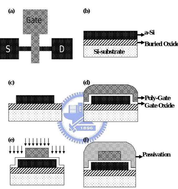
2-1 Fabrication and Structure of Nanowire Devices
Figure 2-1(a) is the top-view of NW devices. The remaining graphs in Fig. 2-1
are cross -sectional views along Line AB . All devices in this work were fabricated
on bare silicon substrate capped with a 150nm-thick wet oxide. First, a 50nm
nitride/100nm TEOS stacked layers were deposited by low pressure chemical vapor
deposition (LPCVD) [Fig. 2-1(b)]. Then, time-mode reactive plasma etching was
applied to define nitride patterns [Fig. 2-1(c)]. Because of the low etch selectivity
between nitride and TEOS in the etch recipe used, the etching time should be
carefully controlled to prevent excessive TEOS lost in this step. After nitride
patterning, wet etching was used to remove the exposed TEOS. The TEOS etch depth
2-1(d)]. Next, a 100nm undoped amorphous silicon (a-Si) was deposited [Fig. 2-1(e)].
By taking advantage of the excellent filling capacity of LPCVD process, the cavities
formed in last step could be refilled by the deposited a-Si. Afterwards, an annealing
step was performed at 600oC in N2 ambient for 24 hours to transform the a-Si into
polycrystalline phase. Subsequently, source/drain (S/D) implant was carried out by P+
implantation with an energy of 30 keV and a dose of 1x1015 cm-2. Note that the S/D
photoresist patterns were generated by a standard I-line lithography step. The main
split conditions of this work were determined by the following steps. For the first type
of structure, denoted as structure 1(S1), an anisotropic plasma etching was performed
to remove the poly-Si not protected by the nitride [Fig. 2-1(f-1)]. Poly-Si films that
filled the previously-existing cavities would be left intact since they were protected by
the nitride in the dry etching step. Hence, nanowire channels were simultaneously
formed at this step in a self-aligned manner. Note that for the S1 devices, the nitride
layer was kept after the etching step, so that only one side of the NW channel is
modulated by the gate, as shown in Fig.2-1(g-1). For the second type of structure,
denoted as structure 2 (S2), the remaining nitride hard mask was subsequently
removed by hot H3PO4 after the poly-Si etching [Fig. 2-1(f-2)]. By continuously
etching TEOS by a diluted HF (DHF) solution with controlled etching time, the third
all structures were combined and capped with a 20nm TEOS gate oxide and a 100nm
in-situ-doped poly-Si gate [Fig. 2-1(g-1) to (g-3)]. It is worth noting that the resultant
S2 and S3 devices have two and three surfaces of the NW channel, respectively,
modulated by the gate. Also note that no additional S/D dopant activation step was
necessary. This is because the depositions of TEOS and poly-Si films were performed
at temperatures higher than 700oC and the process time was sufficiently long to for
dopant activation purpose. After the n+ poly-Si gate patterning, all devices were
passivated with a 250nm-thick TEOS layer. Contact holes and test pads were formed
by standard metallization steps. Finally, the fabrication was completed by a NH3
plasma treatment for 2 hours.
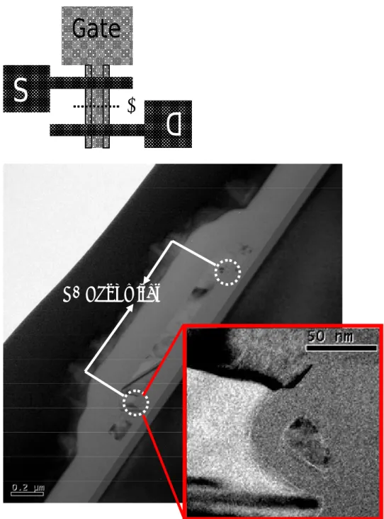
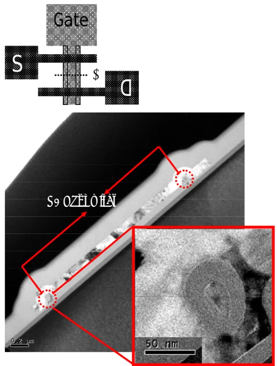
Figures 2-2 and 2-3 show the cross-sectional-view TEM picture of an S2 and S3
device along Line AB . It can be seen that the shape of NWs is nearly a quarter circle
and the dimensions and shapes of S2 and S3 are similar to each other even though
different etch steps were performed to them. The channel width of S1, or the gated
vertical edge of the nanowire, is about 35nm for each nanowire channel. For S2 and
S3 devices, the channel width is increased to 55 and 100nm, respectively, owing to
the fact that additional nanowire edges are incorporated as the conductive channel.
Since there are two NWs in one device, the effective channel width is doubled to 70,
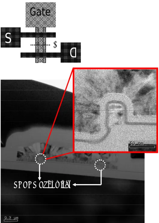
In this study, we also modified the fabrication of S3 devices to fabricate
SONOS-type devices, as shown in Fig. 2-4. First, a nitride(50nm)/TEOS(40nm)
stacked layers were capped on the thermal oxide layer [Fig. 2-4(b)]. Then we defined
dummy nitride/TEOS patterns by anisotropic plasma etching [Fig. 2-4(c)]. DHF
etching was carried out in subsequent step to remove the TEOS layer with high
selectivity to both nitride and thermal oxide, and rectangular recessed cavities were
formed at sides of the dummy patterns [Fig. 2-4(d)]. Following steps were the same as
that in the fabrication of S3 devices [Figs. 2-4(e) to (g)] except for the use of an ONO
stacked gate dielectric, instead of the single TEOS oxide layer [Fig. 2-4(h)] and the
skip of plasma treatment. The ONO layer consists of a 4nm-thick TEOS oxide as the
tunneling oxide, a 7nm-thick nitride as the charge trapping layer, and a 13nm-thick
TEOS oxide as the blocking oxide. Figure 2-5 shows the cross-sectional TEM picture
of an NW SONOS device along Line AB of the top layout shown in the same figure.
It can be seen that the shape of NWs is nearly rectangular with rounding curvature
corner and the dimensions are around 25 and 40nm for the NW width and height,
respectively.
2-2 Fabrication and Structure of Planar Devices
study. The fabrication process was similar to that of conventional TFTs, so the process
would be described only briefly. Figure 2-6(a) is the top view of a planar device.
Briefly, the fabrication began with the deposition of a 60nm-thick undoped a-Si film
on the surface of a thermal oxide capping on a Si wafer. An anneal step was
performed at 600oC in N2 ambient for 24 hours to transform the a-Si into poly-Si [Fig.
2-6(b)]. After S/D and channel region were defined [Fig. 2-6 (c)], a 20nm-thick TEOS
gate oxide and an in-situ-doped poly-gate were deposited [Fig. 2-6(d)]. Afterwards,
gate electrode formation and self-aligned S/D implant were carried out [Fig. 2-6(e)].
Finally, the deposition of passivation layer [Fig. 2-6(f)], the formation of test pads,
and NH3 plasma treatment were performed, similar to the NW devices.
For SONOS-type planar devices, the gate dielectric consists of an ONO layer of
4/7/13 nm. Other steps were nominally identical to MOS-type devices except for the
CHAPTER 3
Characteristics of MOS-Type Devices
One the most important criteria to weigh the characteristic variation of
MOSFETs is the threshold voltage (VTH). So to begin with, we will present the
fundamental notion about standard deviation of VTH in this chapter. Then our
observations on NWs fluctuation will be examined and compared with the developed
models.
3-1 Theory about the Standard Deviation of Threshold
Voltage
Just as specified in Section 1-2, dopant counts in channel region unceasingly
decrease with device scaling, and may fall less than few hundreds in nano-scale
CMOS devices. Discrete random dopant distribution in depletion region is regarded as
the primary source to induce VTH deviation especially in scaled MOSFETs [23]-[25].
To simplify the model, we assume that all parameters are kept constant in the
deduction, other than the dopant distribution. As usual, VTH can be expressed as
OX DEP S FB TH C Q V V = +φ − , (Eq. 3-1)
channel, QDEP is the charge within the depletion region, and COX is the capacitance of
gate oxide. The last term is directly related to dopant distribution in the depletion
region, which causes the essential variation in VTH. According to Takeuchi’s model
[36], VTH shift (∆VTH) can be described as
) 1 ( 0 DEP OX DEP TH W x C Q V = ∆ × − ∆ . (Eq. 3-2)
This model is based on Fig. 3-1(a), which assumes that additional charge sheet
(∆QDEP) at position “x0” within maximum depletion width (WDEP) would cause
surface potential shift and hence VTH change. In Fig. 3-1(b), solid line means original
electrical field in the depletion region induced by substrate doping (NSUB) without any
extra charge and the original surface electrical field is E0. When ∆QDEP is added, the
electrical field is converted into dash line in order to balance the voltage drop at “x0”
and the surface electrical field has an increment of ∆E. The surface potential
difference caused by electrical field variation is the cause of VTH shift.
To calculate standard deviation of VTH (σVTH ), we should consider first.
Here we suppose that in the depletion region is binomial distribution, and
appearance percentage and probability are comparatively less as compared with N DEP Q ∆ DEP Q ∆ SUB.
Thus the standard deviation of ∆QDEP (σ∆QDEP) at “x0” can be approximated by
Poisson’s statistics [37], which is approximated by
LW dx LW x N q QDEP SUB ) ( ) ( = ∆ σ , (Eq. 3-3)
where W is the gate width and L is the gate length. σVTH can be obtained by
substituting Eq. 3-3 into Eq. 3-2 and integrating all the contribution of in the
depletion region from x=0 to x= W
DEP Q
∆
DEP. The result is
LW W N C q V EFF DEP OX TH 3 × = σ , (Eq. 3-4)
where NEFF is the average substrate doping concentration inside the depletion region,
which is equal to
∫
− = DEP W DEP DEP SUB EFF dx W x W x N N 0 2 ) 1 ( ) ( 3 . (Eq. 3-5)From Eq. 3-4, we can see that σVTH is inversely proportional to the square root of
the product LW. The result shows that the variation of VTH is larger as device becomes
smaller.
3-2 Comparisons of Basic Transfer Characteristics
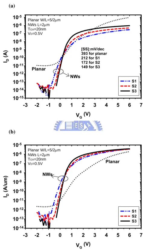
Figure 3-2(a) shows the ID-VG curves of planar and the three kinds of NW
devices. All measured devices have channel length of 2µm and gate oxide thickness of
20nm. It can be seen that all NW devices depict better subthreshold swing (SS) than
planar devices. Among the three kinds of NW devices, the S3 split which has its NW
channels surrounded by the gate exhibits the best SS and the highest on-current, while
worst SS and the lowest on-current. The improvement of SS for the S3 device can be
ascribed to the improved surface-to-volume ratio of its NW structures. S3 device also
has the highest on-current because of its largest effective channel width. Furthermore,
by normalizing the drain current to the channel width, we re-plot the ID-VG curves in
Fig. 3-2(b). Clearly the NWs devices possess higher on-current and lower off-current
than the planar one, hence the Ion/Ioff ratio is higher for NW devices.
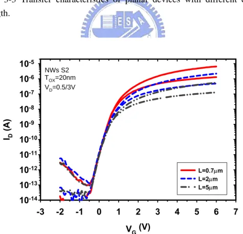
Figures 3-3 and 3-4 show the transfer characteristics of planar and S2 NW
devices, respectively, with different channel length. The ID-VG curves of planar
devices shift as channel length varies, indicating that VTH, SS, and on/off currents are
strongly related to the channel length. This condition is different for NWs as shown in
Fig. 3-4, in which only on-current significantly increases with reduced channel length.
The drain induced barrier lowing (DIBL) is obvious for planar device with channel
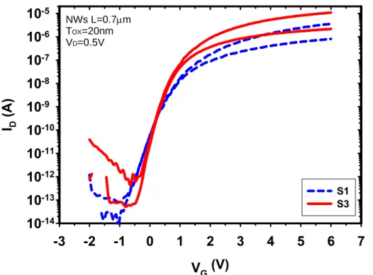
length of 0.7µm. Figure 3-5 shows the transfer curves of S1 and S3 with channel
length of 0.7µm. Unlike the planar counterpart, the DIBL phenomenon is negligible
for the NW devices, which can be attributed to their ultra-thin channel body and much
improved gate controllability.
3-3 Characteristic Variation of Nanowire Devices
Before discussing the experimental results, several important parameters used in
the coming content are revealed first. As shown in Figs. 2-2 and 2-3 and discussed in
Section 2-1, the channel widths of measured devices are 70, 110, and 200nm for S1,
S2, and S3, respectively. For every structure, the devices with three channel lengths of
0.7, 2, 5µm were characterized. In other words, we have investigated nine groups of
devices with different channel width/length in this work. For the purpose of studying
the fluctuation of device performance, we measured thirty devices for each split. Generally, we applied standard deviation (σ ) to judge the variation of samples with
the formula
∑
= − = N i i x x N 1 2 ) ( 1σ , where N is the total numbers of samples, is the
value of individual sample, and
i
x
x is the mean value of all samples. Next, we have to
settle on how to define VTH. For MOSFETs, the VTH is defined by
2
D TH A
V
V =V − ,
where VA is the gate voltage coinciding with the maximum value of transconductance
(gm). Since the max gm of poly-Si TFTs is sometimes not so easy to decide due to the
low carrier mobility, here we instead determine VTH by the constant drain current
method with the following expression:
V V L W nA I G TH D D V V 5 . 0 , 10 × = = = .
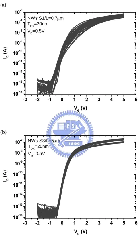
First, we select two series devices to show the ID-VG characteristics. Figures
3-6(a) and (b) are the ID-VG curves of thirty devices from S1 split with channel length
devices with the smallest width and length within our samples in Fig. 3-6(a) have
more apparent fluctuations than the ones with the largest width and length in Fig.
3-6(b). Figure 3-7(a) shows the VTH distribution of different NW structures with
channel length of 2µm. It can be seen that S3 split depicts the narrowest VTH
distribution, while S1 has the widest distribution. Figure 3-7(b) shows VTH
distribution for S2 split with different channel length. We can see that the device with
channel length of 0.7µm depicts wider distribution than devices with longer channel
length (i.e., 2 and 5µm).
Next, we show all measured results of nine groups of devices by transparent
graphic method with VTH mean value and the standard deviation of VTH (σVTH ). In
Figures 3-8(a), (b), and (c), the mean value of VTH of different structures are plotted
for channel length of 0.7, 2, and 5µm, respectively. Note that the error bar represents
TH V
σ . While in Figures 3-9(a), (b), and (c), the mean value of VTH versus channel
length is plotted for S1, S2, and S3, respectively. All of the splits in Figs. 3-8 and 3-9
show the identical trend in σVTH , i.e., when the channel width and/or length increases,
TH V
σ decreases. As described in Section 3-1, the discrete random dopant in depletion
region is regarded as the main source to induce the VTH fluctuation. In our study, no
intentional channel doping was performed to the poly-Si. Nevertheless, the trapping
in the bulk CMOS devices [38] since their charge state is affected by the gate bias and
may affect VTH. To verify this assumption, we plot σVTH versus
LW
1 in Fig.
3-10, in which the experimental data of nine groups of NW devices are fitted with one
solid line, while the data of each NW structure (i.e., S1, S2, and S3) are fitted with the
dashed lines. Note that full depletion of the channel is expected because of the
sufficiently small dimension of our NWs. Figures 2-2 and 2-3 show that the three NW
structures almost possess the same cross-sectional dimensions in the channel region,
hence S1 with only one side of its NW channels gated has the thickest effective
depletion width. On the other hand, the S3 device has a gate-all-around (GAA)
configuration, thus has the thinnest effective depletion width. Therefore, the slope of
the fitting lines for S1 is the highest, S2 falls in the middle, and S3 is the lowest. Such
trend is consistent with the theory depicted by Eq. 3-4.
Figure 3-10 also shows the σVTH of planar devices. The channel width/length
of the measured planar devices is 5/0.7, 10/2, and 20/5µm. The σVTH of planar
devices is higher than that of NWs evidently, which may be ascribed to the much
thicker depletion region of the planar device. The dashed line next to the fitting line
for planar devices is constructed based on the assumption that the planar devices have
channel thickness of 20 nm, similar to that for S1 according to TEM pictures [Figs.
result shows that the σVTH of S1 split is still much smaller than that of planar
devices with similar channel thickness. This might be caused by the insufficient
plasma treatment for planar devices. Most defects in NW channel region can be
passivated and become inactive during the two-hour NH3 plasma treatment due to
high surface-to-volume ratio of NWs. For planar devices, however, the two-hour
duration is not sufficient for plasma to penetrate into entire channel region to repair
the defects because the channel volume is relatively large. Hence the deviation of
planar devices is higher than that of NWs.
3-3-2 Variation of Subthreshold Swing
In addition to VTH, we also plot the standard deviation of SS ( SSσ ) for devices
of different channel length and width. Figures 3-11(a), (b), and (c) show the mean
value of SS and SSσ of the three NW structures for channel length of 0.7, 2, and
5µm, respectively. It can be seen that SS and SSσ decrease when effective channel
width increases from S1 to S3 for a fixed channel length. However, as we plot SS and
SS
σ versus channel length, as shown in Figs. 3-12(a), (b), (c), it can be seen that the
mean values of SS and SSσ seem not to strongly depend on the channel length. But
we can see that the discrepancy of mean value of SS and SSσ between different
channel lengths is largest for S1 [Figs. 3-12(a)] and smallest for S3 [Figs. 3-12(c)].
channel region, which promotes the control ability of gate and then reduces the
deviations of SS mean value and SSσ among different channel lengths. Hence the
CHAPTER 4
Characteristics of SONOS-Type Devices
For non-volatile semiconductor devices such as electrically erasable
programmable read only memories (EEPROMs), several important parameters
including P/E speed, data retention, and endurance need to be carefully considered. In
this chapter, we will first review the basic P/E mechanisms and reliability issues. Then
the experimental results on the fabricated NW SONOS devices will be presented and
discussed.
4-1 Program/Erase Mechanisms of SONOS Flash Memory
4-1-1 Channel Hot Electrons Injection
Several hot-carrier injection (HCI) mechanisms such as channel hot electrons
injection (CHEI) [40], drain avalanche hot carrier (DAHC) [41] and substrate hot
electrons injection (SHEI) [42] have been widely investigated for non-volatile
memory applications. Among these mechanisms, CHEI is often applied to flash
memory. Hence the fundamental theory of CHEI will be reviewed below.
As the device channel length is scaled down, the hot-carrier effects (HCE) [43]
scaled down. It was considered that HCE would be disastrous for submicron
MOSFETs when the hot-carrier effects were first discovered in the seventies.
However, it was serendipitous that, if properly utilized, HCE could turn from disaster
to asset. A case in point is that many flash memory were programmed by hot electrons
from HCE.
As illustrated in Fig. 4-1(a), HCE occurs because of high lateral electrical field
(EL) in channel. While high gate voltage (VG) and drain voltage (VD) are applied, in
generalVD ≥VDSAT =VG−VTH , pinch-off occurs close to drain region. When gate
length (L) shrinks into submicometer while maintaining the same VCC, lateral
electrical field in the pinch-off region increases dramatically for
L V V E D DSAT L − = .
High EL will accelerate transport electrons in the pinch-off region. Electrons can
obtain sufficient energy and become “hot carriers”, known as channel hot electrons
(CHE).
The CHEs with sufficient energy may cause impact ionization, and create extra
electrons named secondary electrons (2nd e-). The CHEs or 2nd e- drift into drain will
contribute to drain current. If these hot electrons overcome energy barrier and be
injected into gate dielectric [Fig. 4-1(b)], they contribute to the gate current, which is
well understood by “lucky electron model” [44]. On the other hand, holes injection is
we can cleverly employ CHEI to achieve programming purpose for non-volatile
memories.
4-1-2 Fowler-Nordheim Tunneling
In the classical theory, electrons in the channel region are forbidden to tunnel
through gate dielectrics into gate electrodes or other states such as n-region of
SONOS structures when carrier energy is lower than the barrier height [Fig. 4-2(a)].
However, as gate oxide thickness is sufficiently thin, the quantum tunneling
phenomenon will occur easily, and can be categorized into the direct tunneling mode
[45] and the Fowler-Nordheim tunneling (F-N tunneling) mode [46].
Electrical field built up across gate oxide (EOX) can be represented by
OX OX OX
t V
E = where VOX and tOX represent voltage drop in oxide region and oxide
thickness, respectively. If VOX is higher than the band-offset (q ) of Si substrate and φ
oxide, electrons in Si channel may tunnel into the conduction band of oxide through
triangular barrier as illustrated in Fig. 4-2(b). Electrons in the conduction band of
oxide will be accelerated by high field and injected into gate. This mechanism is
called F-N tunneling, which was named after Fowler and Nordheim who first reported
the phenomenon in 1928. The difference between direct tunneling and F-N tunneling
“directly” when VOX is lower than band-offset as show in Fig. 4-2(c). The damage on
dielectric caused by direct tunneling is less sever than F-N tunneling due to the fact
that the injecting electrons do not present in the conduction band of the gate dielectric.
But in general, this mechanism leads to a leakage much higher than the F-N process at
a fixed field strength and is therefore not preferred. Because direct tunneling
dominates when oxide thickness is less than 3nm, such a thin oxide is not suitable for
flash memory applications due to retention and reliability issues which will be
discussed in the following section.
4-1-3 Band-to-Band Tunneling
For nano-scale MOSFETs, gate induced drain leakage (GIDL) is a major part of
off-state leakage current. Similar to CHEI, we may take advantage of such
phenomenon and turn it into a useful technique in the operation of flash memory.
As illustrated in Fig. 4-3(a), GIDL is attributed to band-to-band tunneling (BTBT)
in n+ drain region overlapped by the gate region [47]. When a highly negative voltage
relative to n+ region is applied to the gate, deep depletion will occur within n+ area
next to the interface of oxide and silicon substrate. Deep depletion with serious band
bending will promote electron BTBT from valence band to the conduction band in the
promote BTBT. At the same time, holes will be left in the valence band and
accelerated by the strong electrical field. Portion of these accelerated holes may be
attracted by the negative gate voltage and injected into gate oxide contributing to the
gate leakage current [Fig. 4-3(b)].
4-1-4 Program/Erase Principle of the NW Devices
Just as mentioned in previous sections, there are several approaches for P/E
operation in flash memory based on the device configuration. For our devices,
channel is formed with poly-Si and electrons transporting in channel may be scattered
by grain boundaries of poly-Si. Hence it is difficult for electrons to obtain high energy
during transportation and become “hot” enough. So CHEI is not appropriate for
programming operation in the poly-Si NW devices. Hence we decide to employ the
F-N tunneling for programming in this work. For erasing, both F-N and BTBT are
employed and studied.
4-2 Reliability of SONOS Flash Memory
4-2-1 Retention
Retention is a measure of the sustained time for storage of charges in the
charge lost events. For commercial products, the standard retention time is 10 years
with window larger than 0.5 V.
All possible data loss paths mentioned in this section are shown in Fig. 4-4. In
general, two kinds of data loss mechanisms in SONOS flash memory can be
categorized. The first one is Frenkel-Poole mechanism [48]. Frenkel-Poole emission
can be explained by the movement of trapped charges from site to site with level
inside the bandgap (symbol 1 in Fig. 4-4), especially when an electric field is applied.
The injected electrons due to programming are trapped in the nitride, and will raise
the potential of the trapping site. The build-up of local field may boost the movement
of carriers toward the sites located at lower energy levels. As electrons are pushed to
the edge of the nitride layer and near the nitride/oxide interface, the barrier width
relative to the channel narrows as compared with the original position, and tunneling
process may occur (see discussion in the next paragraph). This phenomenon
frequently takes place when a material contains many defects acting as trapping and
de-trapping centers.
The other data loss mechanism is tunneling effect. Electrons in nitride trapping
states can tunnel into the conduction band of Si-substrate (trap-to-band, symbol 2 in
Fig. 4-4) or inject into the interface traps between Si-substrate and tunneling oxide
may push electrons to the edge of the nitride layer, which promotes the tunneling
probability. Not only electrons lost blur data, but also holes in the valence band of
Si-sub tunnel into trapping centers of nitride (band-to-trap, (symbol 4 in Fig. 4-4))
does. [49]
In general, the thickness and quality of tunneling oxide in SONOS devices has
evident influence on data retention. Thin tunneling oxide will lead to a fast P/E rate,
but data storage capacity will decrease due to the shorter tunneling length. With
respect of oxide quality, if there are defects contained in the tunnel oxide,
traps-assisted-tunneling will further speed up the data lost rate. These all challenge
data retention of SONOS flash memory.
4-2-2 Endurance
Another reliability topic is endurance, which is a measure of cycle times that
devices can endure will still retain acceptable P/E window to make devices work
normally. In general, the basic requirement for endurance of flash memory is 106 P/E
cycling times. Fortunately, the endurance requirement will be relaxed when devices
are scaled along with the increase in memory density [50]. For high-density memory,
every cell has less probability to receive P/E cycles because the cell in a memory
accessed. Hence, endurance standard can be lessened from 106 for 16MB to 104 for
4GB.
Programming and erasing operations of flash memory are performed with a very
high electric field. Hence tunneling oxide and trapping layers must be durable to the
operations. As described in Chapter 1 and last section [31][32], the SILC is a main
issue associated with floating-gate flash memory. There are many defects generated in
tunneling oxide region during P/E cycles. These defects act as the sites for
traps-assisted-tunneling and data lost path. So all electrons stored in a “conductive”
floating-gate will leak out through these defects. On the other hand, electrons are
stored in discrete traps in the nitride layer of SONOS, so these electrons will not lose
entirely due to the “insulating” storage layer. This is one important reason for the
SONOS to be regarded as a promising candidate for next-generation flash memory.
In order to reduce stress-induced damage in the tunneling oxide, operation
voltage must be reduced. However, there is a trade-off between P/E speed and applied
voltage, so we have to optimize all related parameters such as the thickness of each
composed layer in the ONO stack, P/E modes, tolerable operation time, etc.
4-3 Program/Erase Characteristics
As mentioned in previous section, the SONOS devices in this work are
programmed and erased by F-N tunneling. For programming, both source and drain of
the fresh device are grounded, and the gate is applied a positive voltage to induced
voltage dropped in ONO region to achieve F-N tunneling. For erasing, the device is
programmed beforehand with 3V shift of VTH relative to the fresh state [Fig. 4-5].
Then the gate of the programmed device is biased with a negative voltage, while
source and drain are both grounded. As shown in Fig. 4-5, the ID-VG curve of a
programmed NW SONOS device is nearly parallel to that of fresh state.
Figure 4-6 shows the VTH shift versus programming time of NW SONOS with
gate bias of 11V, 12V, 13V, and 14V, respectively. For simplicity, the VTH is defined as
the gate voltage at drain current of 1 nA. For a fixed period, the VTH shift increases
with increasing gate bias. It can be seen that memory window of 3V can be achieved
within 1 millisecond (ms) with applied voltage of 14V. We utilize this operation
condition to program fresh devices for investigation of erasing characteristics. Figure
4-7 is the result of VTH shift as a function of erasing time with gate bias of -9V, -10V,
-11V, respectively. The VTH shift increases with increasing gate voltage and/or
operation time. It can be seen that the rate of VTH shift slows down when erasing time
is longer than 100ms with gate bias of -11V. During the erasing process, the amount
oxide also reduces. Therefore the erasing capability weakens and erasing speed is
retarded accordingly.
4-3-2 Program/Erase Characteristics of Planar Devices
In Chapter 3, we have shown transfer characteristics of planar device and NWs.
It is obvious that NW devices possess better gate control ability and stable reliability.
Hence it is predictable that NWs will have better characteristics than planar SONOS.
Figure 4-8 shows the programmed and erased states of both NWs and planar SONOS,
which verifies our predictions. Here we define erased state as “on” state, programmed
state as “off” state, and the reading voltage is set at 2.5V. With the same memory
window of 2.5V, the Ion/Ioff ratio of NW devices is higher than that of planar SONOS.
This diversity can be attributed to better SS and less leakage current of NW devices.
Figure 4-9 compares the programming characteristics of planar and NW SONOS
devices with identical ONO thickness. To compare the programming capability, we
apply the same gate bias of 14V to both planar and NW devices. For NWs, VTH shift
is over 1V when the programming time is merely 1 microsecond (µs). On the contrary,
VTH shift of planar devices is less than 0.1V even when the programming time
increases to 10ms. In order to have the same VTH shift as the NW device at 10ms, a
in erasing characteristics, as shown in Fig. 4-10. If we apply gate voltage of -11V to
the planar device for 1s, the programmed device only exhibits negligible shift. To
attain comparable erasing speed to that of the NW device biased with gate voltage of
-11V, the gate bias of planar devices must be raised to -20V.
Irrespective of programming or erasing operation, the above results show that the
NWs devices exhibit better efficiency than planar counterparts. As shown in Fig. 2-5,
the cross-sectional shape of the tri-gated NW channel is nearly rectangular
configuration with rounding curvature corners. Here we consider the results of NW
SONOS devices with round NW channel and GAA configuration reported in a recent
publication [51]. The superiority of NW devices in P/E speed over the planar structure
is also observed in that previous work, so we refer to their deduction based on the
band diagrams shown in Fig. 4-11 to explain our experimental findings. Figure
4-11(a) shows the band diagrams of planar and NW SONOS devices with identical
ONO thickness and gate bias under programming operation. The solid line and dash
line represent the potential profile of NW and planar devices, respectively. It can be
seen that the voltage dropped across tunneling oxide in GAA NWs is higher than
planar devices due to its high curvature, hence the barrier width in tunneling oxide is
thinner with respect to planar devices. Because the tunneling probability increases as
higher than that of the planar one when the applied gate bias is the same. Similar
situation occurs for erasing operation, as shown in Fig. 4-11(b). Therefore, GAA NW
devices exhibit much better P/E efficiency than planar devices. Although the shape of
the NW cross-section characterized in this study is different from the round shape in
the previous work, we believe the rounded corner region should behave similarly as
that described in Fig. 4-11, and thus dramatically promote the P/E efficiency.
4-4 Reliability Characteristics of Nanowire Devices
4-4-1 Retention Characteristics
Before discussing the reliability topic of NW SONOS devices, we briefly explain
the procedural rules used for retention and endurance measurements in this work.
Figure 4-12 shows ID-VG curves of SONOS devices before and after a few cycles of
P/E operation. The solid line in the left is the fresh-state characteristics. We apply gate
voltage of 14 V for 1ms to perform the first-time programming to attain VTH shift of
3V. Then in the second operation, the gate is biased at -11V for 50ms to erase the
programmed device and cause the VTH shift of -2.3V. In order to reach the same
programmed state as the first operation, we apply gate bias of 13V instead of 14V for
1ms to program the device again. For the fourth and fifth operations and beyond, the
Except for the first programming, the P/E specifications of other cycles make the
SONOS in stable programmed and erased states, which are “real-life situations” in
practical products. Hence the parameters employed in this section are according to the
P/E specifications of “real-life situations.”
The data retention characteristics of fresh devices are shown in Fig. 4-13. If we
program the devices by gate bias of 13V for 1ms, and -11V with 50ms for erasing, the
memory window can be larger than 0.5V after 10 years at room temperature. Figure
4-14 is the data retention measured at 25oC, 55oC, and 85oC, respectively. No matter
in programmed or erased state, the data storage ability is stable and the temperature
dependence of memory window at 10 years is weak. This phenomenon is reasonable.
The data lost path of SONOS discussed in previous section is mainly through
Frenkel-Poole emission and tunneling effect. Hence the temperature dependence is
not evident.
4-4-2 Endurance Characteristics
There are two P/E specifications applied to endurance tests, as indicated in Fig.
4-15. The results show that the stressing cycles can be more than 104 with acceptable
memory window. Nevertheless, window opening is observed in our measurement. The
specifications. As stressing cycles increasing, the windows extend from 1.39 and
2.29V to 1.98 and 2.96V respectively.
During the stressing process, electrons tunnel through bottom oxide between
channel and nitride backwards and forwards. Hence tunneling oxide will directly
affect the P/E efficiency, if there are any changes in its properties during stressing.
Since the thickness of blocking oxide in this work is quite thick (13nm), electrons
barely tunnel into the gate and thus we ignore the influence of this particular charge
loss path.
First, we measured and inspected the evolution of subthreshold characteristics
during P/E operations. If there are interface states created during the operation, VTH
shift may mainly come from the increase in subthreshold swing (SS). Figure 4-16
show ID-VG characteristics of the device coinciding with the measured points shown
in Fig. 4-15 with P/E specification of 13V1ms/-11V50ms. It can be seen that in the
programmed state, the SS other than the first time programming becomes worse.
Because we define VTH at ID=1nA, the VTH shift in programmed state comes from SS
degradation. On the other hand, the change of SS in erased state is not significant, and
thus the SS variation has a small effect on the VTH shift in the erased state.
Next, we measured the retention characteristics again to examine the quality of
subjecting to one (fresh) and 104 P/E cycles with P/E specification of
13V1ms/-11V50ms. Here we discuss the programmed and erased state separately. For
programmed state, if the window opening is caused by additional electrons trapped in
the tunneling oxide during P/E cycles, data loss will be more severe. Because the
tunneling length of electrons trapped in tunneling oxide is shorter than that in nitride,
electrons will escape more easily. Compared with fresh devices, the VTH of stressed
devices does not show apparent change in the rate of VTH lowering in programmed
state in Fig. 4-17. Therefore, we can confirm our contention in last paragraph that VTH
shift in programming retention characteristics come from SS degradation.
For erased state, Figure 4-17 shows that the erased device after stressing has
evident positive shift in VTH in seconds and then reaches a steady state. During
stressing cycles, holes would inject into nitride to accomplish erasing operation and
some holes may stay in tunneling oxide. These holes would result in VTH decrease as
with a fresh device without holes injection. This is the origin of window opening in
erased state after stressing. When we stop applying negative bias for erasing operation,
these holes stored in the tunneling oxide may escape easily and lead to recovery of
CHAPTER 5
Conclusion and Future Work
5-1 Conclusion
In this thesis, without resorting to advanced lithographical tools like e-beam
direct writers, we propose a simple and flexible way to successfully fabricate NW
devices with three different types of MG configurations. Furthermore, we also
modified the fabrication to fabricate tri-gated SONOS devices with nearly rectangular
configuration.
Compared with planar devices, the improvements in SS, leakage, DIBL, and
on/off ratio for NWs are verified in our experimental results. These excellent NW
characteristics can retain even with shrunk channel length. Among our three NW
structures, the S3 split which has a gate-all-around configuration exhibits the best gate
controllability, hence it possesses the most prominent performance in nearly all
aspects of device characteristics. For device variation issue, the standard deviation of
VTH is shown to be inversely proportioned to WL , which is consistent with the
planar CMOS theory. Moreover, the fluctuation of planar devices is higher than that
relatively wider channel and thus larger channel volume that needs a longer time to
effectively passivate the defects.
Regarding the SONOS devices, NW structures have apparent improvement on
P/E efficiency as compared with planar devices, which can be attributed to the
increase of curvature of the NWs. Though the P/E speed of NWs is better than that of
planar devices, the erasing speed is somewhat slower owing to the rather thick
blocking oxide. The retention measurements show that the memory window can be
larger than 0.5V after 10 years at 85oC. For endurance test, the devices can sustain
P/E cycles for more than 104 times and maintain acceptable memory window in
retention test.
5-2 Future Work
When the channel length reduces, our NWs still possess good gate control
abilities. Therefore, if we can design a layout with increased NW count in a unit area
to provide sufficient current drive, it is believed that NW-TFTs will become a
promising candidate for future applications.
The fabricated S3 device is a GAA NW, but its shape is not preferred for
electrical characteristics because of the sharp corners. Hence we have to improve the
NW structure and make it close to a circle, which is suitable for the applications of
blocking oxide for our SONOS devices to reduce the operation voltage and/or to
increase the P/E speed.
. In this study, we have demonstrated many important and interesting results
about NW characteristics. Nevertheless, it is a pity that we don’t have a complete
model to explain the characteristics of the NW devices. Therefore, performing more
REFERENCES
[1] Ran-Hong Yan, Abbas Ourmazd, and Kwing F. Lee. “Scaling the Si MOSFET:
From Bulk to SOI to Bulk,” IEEE Transactionss on Electron Devices, vol. 39,
no. 7, pp. 1704-1710, 1992.
[2] Tetsu Tanaka, Hirishi Horie, Satoshi Ando, and Shinpei Hijiya. “Analysis of p
Poly Si Double-Gate Thin-Film SOI MOSFETs
+
,” IEDM, pp.683-686, 1991.
[3] Digh Hisamoto, Wen-Chin Lee, Jakub Kedzierski, Erik Anderson, Hideki Takeuchi, Kazuya Asano, Tsu-Jae King, Jeffrey Bokor, and Chenming Hu. “A
Folded-Channel MOSFET for Deep-Sub-Tenth Micron Era,” IEDM, pp. 1032-1034, 1998.
[4] B.S. Doyle, S. Datta, M. Doczy, S. Hareland, B. Jin, J. Kavalieros, T. Linton, A. Murthy, R. Rios, and R. Chau. “High Performance Fully-Depleted Tri-Gate
CMOS Transistors,” IEEE Electron Device Letters, vol. 24, no. 4, pp. 263–265, 2003.
[5] Fu-Lian Yang, Hau-Yu Chen, Fang-Cneng Chen, Cheng-Chuan Huang, Chang-Yun Chang, Hsien-Kuang Chiu, Chi-Chung Li, Chi-Chun Chen, Huan-Tsung Huang, Chih-Jian Chen, Hun-Jan Tao, Yee-Chia Yeo, Mong-Song Lian, and Chenming Hu. “25 nm CMOS Omega FETs,” IEDM, pp. 255–258, 2002.
[6] J.P. Colinge, M.H.Gao, A. Romano-Rodrigeuz, H. Maes, and C. Claeys. “Silicon-On-Insulator Gate-All-Around Device,” IEDM, pp. 595-598, 1990.
S. Deleonibus. “Multiple Gate Devices: Advantages and Challenges,”
Microelectronic Engineering, vol. 80, pp. 378-385, 2005.
[8] Jean-Pierre Raskin, Tsung Ming Chung, Valeria Kilchytska, Dimitri Ledere, and Denis Flandre. “Analog/RF Performance of Multiple Gate SOI Devices:
Wideband Simulations and Characterization,” IEEE Transactionss on
Electron Devices, vol. 53, no. 5, pp. 1088-1095, 2006.
[9] J. Saint-Martin, A. Bournel, and P. Dollfus. “Comparison of Multiple-Gate
MOSFET Architectures Using Monte Carlo Simulation,” Solid-State
Electronics, vol. 50, no. 1, pp. 94-101, 2006.
[10] Xiangfeng Duan, Yu Huang, and Charles M. Lieber. “Nonvolatile Memory and
Programmable Logic from Molecule-Gated Nanowires,” Nano letters, vol. 2, no. 5, pp. 487-490, 2002.
[11] Xiangfeng Duan, Chunming Niu, Vijendra Sahi, Jian Chen, J. Wallace Parce, Stephen Empedocles and Jay L. Goldman. “High-Performance Thin-Film
Transistors Using Semiconductor Nanowires and Nanoribbons,” Nature, vol.
425, pp. 274-278, 2003.
[12] Xiandfeng Duan, Yu Huang, Yi Cui, Jianfang Wang, and Charles M. Lieber.
“Indium Phosphide Nanowires as Building Blocks for Nanoscale Electronic and Optoelectronic Devices,” Nature, vol. 409, pp. 66-69, 2001.
[13] Fernando Patolsky and Charles M. Lieber. “Nanowire Nanosensors.” Materials
today, vol. 8, pp. 20-28, 2005.
[14] Jong-in Hahm and Charles M. Lieber. “Direct Ultrasensitive Electrical
Nanosensors,” Nano Letters, vol. 4, no. 1, pp. 51-54, 2004.
[15] D. Mijatovic, J. C. T. Eijkel and A. van den Berg. “Technologies for
Nanofluidic Systems: Top-Down vs. Bottom-Up — a review,” Lab Chip, vol.
5, pp. 492-500, 2005.
[16] O. H. Elibol, D. Morisette, D. Akin, J. P. Denton, and R. Bashir. “Integrated
Nanoscale Silicon Sensors Using Top-Down Fabrication,” Applied Physics Letters, vol. 83, no. 22, pp.4613-4615, 2003.
[17] Mingwei Li, Rustom B. Bhiladvala, Thomas J. Morrow, James A. Sioss, Kok-Keong Lew, Joan M. Redwing, Christine D. Keating and Theresa S. Mayer.
“Bottom-Up Assembly of Large-Area Nanowire Resonator Arrays,” Nature
Nanotechnology, vol. 3, pp. 88-92, 2008.
[18] W. Haensch, E. J. Nowak, R. H. Dennard, P. M. Solomon, A. Bryant, O. H. Dokumaci, A. Kumar, X. Wang, J. B. Johnson, and M. V. Fischetti. “Silicon
CMOS Devices Beyond Scaling,” IBM Journal of Research and Development, vol. 50, no. 4/5, pp.339-361, 2006.
[19] Siva G. Narendra. “Effect of MOSFET Threshold Voltage Variation on
High-Performance Circuit,” PH. D. Dissertation, Department of Electrical Engineering and Computer Science, Massachusetts Institute of Technology,
2002.
[20] Asen Asenov, and Subhash Saini. “Polysilicon Gate Enhancement of the
Random Dopant Induced Threshold Voltage Fluctuations in Sub-100 nm MOSFETs with Ultrathin Gate Oxide,” IEEE Transactionss on Electron