Characteristics of efficiency droop in GaN-based light emitting diodes with an
insertion layer between the multiple quantum wells and n -GaN layer
S. P. Chang, C. H. Wang, C. H. Chiu, J. C. Li, Y. S. Lu, Z. Y. Li, H. C. Yang, H. C. Kuo, T. C. Lu, and S. C. Wang
Citation: Applied Physics Letters 97, 251114 (2010); doi: 10.1063/1.3531957 View online: http://dx.doi.org/10.1063/1.3531957
View Table of Contents: http://scitation.aip.org/content/aip/journal/apl/97/25?ver=pdfcov Published by the AIP Publishing
Articles you may be interested in
High quality ultraviolet Al Ga N Ga N multiple quantum wells with atomic layer deposition grown AlGaN barriers
Appl. Phys. Lett. 93, 131116 (2008); 10.1063/1.2996566
Enhanced emission efficiency of Ga N In Ga N multiple quantum well light-emitting diode with an embedded photonic crystal
Appl. Phys. Lett. 92, 251110 (2008); 10.1063/1.2948851
Effect of dislocation density on efficiency droop in Ga In N Ga N light-emitting diodes Appl. Phys. Lett. 91, 231114 (2007); 10.1063/1.2822442
Effect of threading defects on InGaN GaN multiple quantum well light emitting diodes Appl. Phys. Lett. 91, 231107 (2007); 10.1063/1.2822395
Efficiency droop behaviors of In Ga N Ga N multiple-quantum-well light-emitting diodes with varying quantum well thickness
Appl. Phys. Lett. 91, 181113 (2007); 10.1063/1.2805197
This article is copyrighted as indicated in the article. Reuse of AIP content is subject to the terms at: http://scitation.aip.org/termsconditions. Downloaded to IP: 140.113.38.11 On: Wed, 30 Apr 2014 07:55:43
Characteristics of efficiency droop in GaN-based light emitting diodes
with an insertion layer between the multiple quantum wells and n-GaN layer
S. P. Chang,1,2C. H. Wang,1C. H. Chiu,1J. C. Li,1,a兲 Y. S. Lu,1Z. Y. Li,1H. C. Yang,2 H. C. Kuo,1,b兲 T. C. Lu,1and S. C. Wang1
1
Department of Photonics and Institute of Electro-Optical Engineering, National Chiao-Tung University, 1001 University Road, Hsinchu 300, Taiwan
2
R and D Division, Epistar Co. Ltd., Science-based Industrial Park, Hsinchu 300, Taiwan
共Received 19 September 2010; accepted 7 December 2010; published online 23 December 2010兲 We have studied the characteristics of efficiency droop in GaN-based light emitting diodes共LEDs兲 with different kinds of insertion layers共ILs兲 between the multiple quantum wells 共MQWs兲 layer and
n-GaN layer. By using low-temperature共LT兲 共780 °C兲 n-GaN as IL, the efficiency droop behavior
can be alleviated from 54% in reference LED to 36% from the maximum value at low injection current to 200 mA, which is much smaller than that of 49% in LED with InGaN/GaN short-period superlattices layer. The polarization field in MQWs is found to be smallest in LED with InGaN/GaN SPS layer. However, the V-shape defect density, about 5.3⫻108 cm−2, in its MQWs region is much higher than that value of 2.9⫻108 cm−2 in LED with LT n-GaN layer, which will lead to higher defect-related tunneling leakage of carriers. Therefore, we can mainly assign this alleviation of efficiency droop to the reduction of dislocation density in MQWs region rather than the decrease of polarization field. © 2010 American Institute of Physics. 关doi:10.1063/1.3531957兴
In recent years, great efforts have been made to improve the performance of GaN-based light emitting diodes共LEDs兲 due to their widespread application in solid-sate lighting, dis-play technology, color printing, and optical storage.1One of the promising approaches is to introduce an additional layer, such as InGaN/GaN short-period superlattices 共SPS兲,2,3 InGaN layer,4,5 or low-temperature 共LT兲 n-GaN layer,6 be-tween the n-type GaN and the multiple quantum wells 共MQWs兲 layers. Several studies have been revealed that such insertion layers 共ILs兲 can release the residual strain in MQWs layer, reduce the V-pits density in MQWs, or im-prove the current spreading in LED.2–6As a result, the quan-tum efficiency and the output power of LED can be en-hanced. However, as the efficiency of LEDs increases, the upcoming challenge is that the quantum efficiency substan-tially decreases with increasing drive current, so-called effi-ciency droop.7 Over the past year, several different mecha-nisms for the efficiency droop have been suggested, including carrier leakage from the active region,8 the effect of the polarization field in the MQWs,9nonuniform distribu-tion of holes,10defect-related tunneling leakage of carriers,11 Auger recombination,12and carrier delocalization.13 Consid-ering the advantages of using the ILs mentioned above, one can expect that the efficiency droop behavior can be allevi-ated in such LEDs with the ILs. But which kind of IL can reduce the efficiency droop more effectively? And what is the major mechanism for this reduction? More detailed in-vestigations are necessary. In this work, we studied the char-acteristics of efficiency droop in GaN-based LEDs with dif-ferent kinds of ILs by performing the electroluminescence, photoluminescence 共PL兲, cathodoluminescence 共CL兲, scan-ning electron microscope, and transmission electron micros-copy共TEM兲 measurements.
The samples in this study were grown on c-plane共0001兲 sapphire substrates by metalorganic chemical vapor deposi-tion. After depositing a 20-nm-thick LT 共550 °C兲 GaN nucleation layer on the sapphire substrate, a 2-m undoped GaN and a 2-m Si-doped 共5⫻1019 cm−3兲 n-type GaN were grown at 980 ° C, followed by an IL and the MQWs active region. Two kinds of ILs were used in this study. One is InGaN/GaN SPS layer, which consisted of 10 pairs of In0.06Ga0.94N layer 共⬃0.9 nm兲 and GaN layer 共⬃1.7 nm兲. The other is 60-nm LT n-GaN layer. Note that both of the ILs are doped with Si共5⫻1018 cm−3兲 and deposited at 780 °C. The MQWs active region consisted of six pairs of GaN bar-rier 共⬃14.2 nm, deposited at 860 °C兲 and unintentionally doped In0.15Ga0.85N well 共⬃3.9 nm, deposited at 780 °C兲. Finally, a 20-nm electron blocking layer with Mg-doped
p-type Al0.15Ga0.85N and a 200-nm Mg-doped p-type GaN layer were grown at 880 ° C. The Mg-dopant concentration is about 1⫻1019 cm−3. For comparison, the same LED structure without the IL was also prepared. After growth, the LED chips were fabricated by regular chip process with in-dium tin oxide current spreading layer and Ni/Au contact metal, and the size of mesa is 300⫻300 m2. Throughout this work, for convenience, we shall refer to LED structures without and with InGaN/GaN SPS and LT n-GaN ILs as reference, type I, and type II LEDs. In addition, in order to investigate the surface morphology of MQWs, three samples without the electron blocking layer and the p-type GaN layer were also grown, denoted as reference, type I, and type II MQWs.
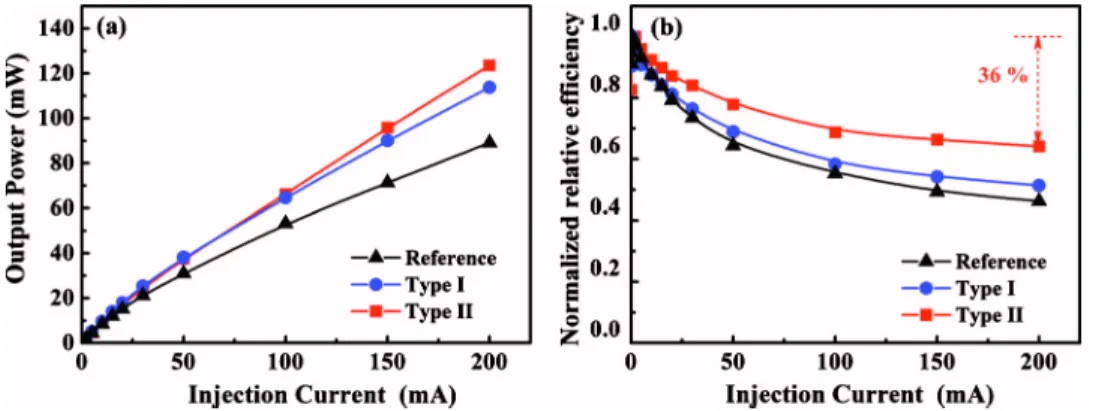
The electrical and luminescence characteristics of the LEDs were measured at room temperature 共RT兲 with a cali-brated integrating sphere. To prevent the self-heating effect, the devices were driven in pulsed mode with 1 KHz fre-quency and 0.1% duty cycle. Figure 1共a兲 shows the output power of the three types of LEDs as a function of injection current. With 20-mA injection current, the output power of type I and type II LEDs are 18.0 and 17.0 mW, respectively,
a兲Electronic mail: [email protected]. b兲Electronic mail: [email protected].
APPLIED PHYSICS LETTERS 97, 251114共2010兲
0003-6951/2010/97共25兲/251114/3/$30.00 97, 251114-1 © 2010 American Institute of Physics
This article is copyrighted as indicated in the article. Reuse of AIP content is subject to the terms at: http://scitation.aip.org/termsconditions. Downloaded to IP: 140.113.38.11 On: Wed, 30 Apr 2014 07:55:43
which are increased by 18% and 11%, as compared with the value of 15.3 mW for reference LED, while the enhance-ments at 200 mA are approximately 28% and 39% for type I and type II LEDs, respectively. These results indicate that not only the light output power has been improved but also the efficiency droop behavior has been changed by using the ILs. To illustrate the droop behavior more clearly, the normalized relative efficiencies of the three types of LEDs are plotted as a function of injection current in Fig.
1共b兲. Then, the efficiency droop can be defined as 共peak −200 mA兲/peak, where peak is the maximum efficiency at low injection current. It is interesting that the efficiency droop in type II LED is only about 36%, which is much smaller than that in type I LED 共49%兲 and reference LED 共54%兲. That is, the efficiency droop behavior can be allevi-ated more effectively by using the LT n-GaN IL.
To figure out the origins of the alleviation in efficiency droop for LEDs with ILs, the power-dependent PL measure-ments excited with a frequency-doubled Ti: sapphire laser at wavelength of 385 nm were first carried out at RT. The laser pulse width was 200 fs and the repetition rate was 76 MHz. The laser beam was focused to a spot with diameter of 50 m. The luminescence spectrum was dispersed by a 0.5 m monochromator and detected by a photomultiplier tube. Figure2 illustrates the emission energy and full width at half maximum共FWHM兲 as a function of excitation power. At an excitation power of 0.02 mW, the emission energies for type I and type II LEDs are 2.819 and 2.815 eV, respec-tively, which is much higher than that of 2.774 eV for refer-ence LED. Meanwhile, the emission energies blueshift with increasing the excitation power in all of the three types of LEDs. Such blueshift can be attributed to two mechanisms: one is the photoinduced carriers screening effect of the po-larization field accompanied by shrinkage of FWHM, the other is the band filling effect with a broadening of FWHM.14,15 As can be seen from Fig. 2共b兲, the FWHM
changes slightly in the low excitation power range 共⬍10 mW兲, indicating the screening effect is dominated in this region. As the excitation power is further increased, the band filling effect becomes dominated because of the signifi-cant broadening of FWHM. Therefore, we analyzed semi-quantitatively the polarization field by fitting the emission energy of PL spectrum 共h兲 in the low excitation power range with a triangular well model14
h= Eg共n兲 − dF共n兲 +
冋
冉
1 me冊 1/3 +冉
1 mh冊
1/3册
⫻冋
9ប 8冑
2F共n兲册
2/3 , 共1兲where the band-gap renormalization and the screening of the polarization field due to nonequilibrium carriers共n兲 are taken into account as Eg共n兲=Eg共0兲−n1/3, and F共n兲=F共0兲
− ned/0, respectively. Here, Eg共0兲 and F共0兲 are the energy
band-gap and polarization field in the unexcited sample 共n = 0兲, respectively, while d, , and me,h are the well width, dielectric constant, and electron- or hole-effective mass. In the calculation, the material parameters are obtained from the literature,16and the excitation power is converted into carrier density using the similar method in Ref. 14. The fitting re-sults are illustrated in Fig.2共a兲by the dashed line. The F0in the reference LED is found to be about 1.21 MV/cm, which is lower than the value 共1.87 MV/cm兲 obtained in similar MQW structure.14 It can be attributed to that our MQWs were grown on thicker n-GaN layer with lower residual strain.17 But for type I and type II LEDs, smaller values are obtained to be 0.62 and 0.66 MV/cm, respectively, implying both two kinds of ILs can release the residual strain for a certainty. The strain reduction effect by ILs has been studied and can be attributed to the suppression of the epiwafer bowing.18 In addition, the InGaN/GaN SPS IL was
demon-FIG. 1.共Color online兲 共a兲 The output powers and共b兲 the normalized relative efficiencies for the three types of LEDs as a function of injection current.
FIG. 2. 共Color online兲 共a兲 The emis-sion energy and 共b兲 FWHM for the three types of LEDs as a function of excitation power.
251114-2 Chang et al. Appl. Phys. Lett. 97, 251114共2010兲
This article is copyrighted as indicated in the article. Reuse of AIP content is subject to the terms at: http://scitation.aip.org/termsconditions. Downloaded to IP: 140.113.38.11 On: Wed, 30 Apr 2014 07:55:43
strated to decrease the epiwafer bowing more effectively, re-sulting in larger a-axis lattice constant of GaN and lower compressive strain in MQW. This agrees with our experi-mental results.
It is well known that the reduction of polarization field in InGaN/GaN MQWs causes less band bending, which in turn, results in higher emission energy, higher radiative recombi-nation, and less electron leakage from the active region.9,15,19 Therefore, it is reasonable that type I LED has the highest light output power at 20 mA and the largest emission energy, due to the smallest polarization field in it. However, it is still difficult to understand why the type II LED, instead of type I LED, does have a rather small efficiency droop.
Further insight investigations were performed by CL and TEM measurements. Although dark spots can be observed on the surface of all three samples from the monochromatic spa-tially resolved CL images 共not shown here兲, the density is found to be decreased from 5.9 to 7.5⫻108 cm−2 in refer-ence MQWs to 5.3⫻108and 2.9⫻108 cm−2, for type I and type II MQWs, respectively. The fluctuation of the value for reference MQWs is due to that some of the dark spots over-lap each other and difficult to figure out. Such dark spots are related to nonradiative centers in the V-defects confirmed by SEM morphology, which is commonly believed to consist of a threading dislocation terminated by a pit in the shape of an inverted hexagonal pyramid.20,21 In this sense, the lower dark-spot density suggests the reduction of dislocation den-sity in the MQWs region of both LEDs with ILs.
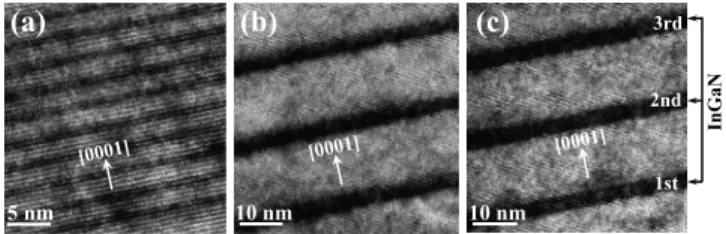
It has been reported that strain in the MQWs and In distribution inhomogeneities in the InGaN well are the main factors responsible for the V-defect occurrence and propagation.20,21 As discussed above, for type I LED, the strain in the MQWs is relatively small. However, from the cross-section high resolution TEM 共HRTEM兲 image in Fig.
3共a兲, one can clearly see slight well width and composition fluctuations in SPS layer. These may not only induce addi-tional V-defects but also influence the subsequent growth of the MQWs layer. It is practical that type I MQWs exhibit rather rough interfaces and apparent nonuniformity of In dis-tribution, as shown in Fig.3共b兲. While for the type II MQWs 关Fig.3共c兲兴, since the LT n-GaN IL dose not contain In, clear
and sharp interfaces can be observed. In addition, the In dis-tribution is more homogeneous especially for the first and the second wells. Therefore, the dislocation density is much lower in the MQWs region of type II LED. Accordingly, the tunneling leakage of carriers from the QW to defect states in barriers is expected to be much smaller in type II LED than that in type I LED, which is considered to be one of the major reasons for the efficiency droop.11 As a result, the
efficiency droop behavior is alleviated more effectively by inserting LT n-GaN layer.
In summary, the efficiency droop behaviors in two types of GaN-based LEDs with InGaN/GaN SPS and LT n-GaN ILs, respectively, were investigated in this work. The power-dependent PL reveals that the polarization field in MQWs is smallest in LED with InGaN/GaN SPS IL. Therefore, the output power at 20 mA共18.0 mW兲 is a little higher than that in LED with LT n-GaN IL 共17.0 mW兲. However, the CL images indicate that the dislocation density in MQWs is much lower in the latter LED. This might be due to that the In distribution is more homogeneous and the interface in the MQWs is extremely sharp after inserting LT n-GaN layer, which is verified by the TEM image. Accordingly, the tun-neling leakage of carriers from the QW to defect states in barriers is expected to be much smaller in LED with LT
n-GaN IL. As a result, the efficiency only drops about 36%
from the maximum value at low injection current to 200 mA, which is much smaller than that of 49% in LED with InGaN/ GaN SPS IL and 54% in reference LED.
The authors would like to thank Dr. T. C. Hsu and M. H. Shieh of Epistar Corporation for their technical support. This work was founded by the National Science Council in Tai-wan under Grant Nos. 3114-M-009-001 and NSC98-3114-E-009-002.
1S. Nakamura, S. Pearton, and G. Fasol, The Blue Laser Diode: GaN Based
Light Emitters and Lasers, 2nd ed.共Springer, New York, 2000兲, pp. 1–9.
2P. C. Tsai, Y. K. Su, W. R. Chen, and C. Y. Huang,Jpn. J. Appl. Phys. 49,
04DG07共2010兲.
3S. J. Leem, Y. C. Shin, K. C. Kim, E. H. Kim, Y. M. Sung, Y. Moon, S. M.
Hwang, and T. G. Kim,J. Cryst. Growth 311, 103共2008兲.
4T. Akasaka, H. Gotoh, T. Saito, and T. Makimoto,Appl. Phys. Lett. 85,
3089共2004兲.
5C. H. Jang, J. K. Shey, C. M. Tsai, S. J. Chang, W. C. Lai, M. L. Lee, T.
K. Ko, C. F. Shen, and S. C. Shei,IEEE J. Quantum Electron. 46, 513
共2010兲.
6R. M. Lin, Y. H. Lin, C. H. Chiang, M. J. Lai, Y. L. Chou, Y. C. Lu, S. Y.
Kuo, B. R. Fang, and M. C. Wu,Microelectron. Reliab. 50, 679共2010兲.
7M. H. Crawford,IEEE J. Sel. Top. Quantum Electron. 15, 1028共2009兲. 8K. J. Vampola, M. Iza, S. Keller, S. P. DenBars, and S. Nakamura,Appl.
Phys. Lett. 94, 061116共2009兲.
9M. H. Kim, M. F. Schubert, Q. Dai, J. K. Kim, E. F. Schubert, J. Piprek,
and Y. Park,Appl. Phys. Lett. 91, 183507共2007兲.
10A. David, M. J. Grundmann, J. F. Kaeding, N. F. Gardner, T. G.
Mihopou-los, and M. R. Krmes,Appl. Phys. Lett. 92, 053502共2008兲.
11N. I. Bochkareva, V. V. Voronenkov, R. I. Gorbunov, A. S. Zubrilov, Y. S.
Lelikov, P. E. Latyshev, Y. T. Rebane, A. I. Tsyuk, and Y. G. Shreter, Appl. Phys. Lett. 96, 133502共2010兲.
12Y. C. Shen, G. O. Mueller, S. Watanabe, N. F. Gardner, A. Munkholm, and
M. R. Krames,Appl. Phys. Lett. 91, 141101共2007兲.
13B. Monemar and B. E. Sernelius,Appl. Phys. Lett. 91, 181103共2007兲. 14E. Kuokstis, J. W. Yang, G. Simin, M. A. Khan, R. Gaska, and M. S. Shur,
Appl. Phys. Lett. 80, 977共2002兲.
15T. Wang, D. Nakagawa, J. Wang, T. Sugahara, and S. Sakai,Appl. Phys. Lett. 73, 3571共1998兲.
16U. M. E. Christmas, A. D. Andreev, and D. A. Faux,J. Appl. Phys. 98,
073522共2005兲.
17L. T. Romano, C. G. Van de Walle, J. W. Ager III, W. Götz, and R. S.
Kern,J. Appl. Phys. 87, 7745共2000兲.
18M. Sakai, T. Egawa, M. Hao, and H. Ishikawa,Jpn. J. Appl. Phys., Part 1
43, 8019共2004兲.
19F. D. Sala, A. D. Carlo, P. Lugli, F. Bernardini, V. Fiorentini, R. Scholz,
and J. M. Jancu,Appl. Phys. Lett. 74, 2002共1999兲.
20I. H. Kim, H. S. Park, Y. J. Park, and T. Kim,Appl. Phys. Lett. 73, 1634
共1998兲.
21D. I. Florescu, S. M. Ting, J. C. Ramer, D. S. Lee, V. N. Merai, A. Parkeh,
D. Lu, E. A. Armour, and L. Chernyak,Appl. Phys. Lett. 83, 33共2003兲.
10 nm 10 nm 5 nm (a) (b) (c) In G aN 1st 2nd 3rd [0001] [0001] [0001]
FIG. 3. Cross-section HRTEM images for共a兲 the SPS layer in type I LEDs, 共b兲 MQWs structures in type I LEDs, and 共c兲 MQWs structures in type II LEDs.
251114-3 Chang et al. Appl. Phys. Lett. 97, 251114共2010兲
This article is copyrighted as indicated in the article. Reuse of AIP content is subject to the terms at: http://scitation.aip.org/termsconditions. Downloaded to IP: 140.113.38.11 On: Wed, 30 Apr 2014 07:55:43