Bistable Resistive Switching in Al
2O
3Memory Thin Films
Chih-Yang Lin,aChen-Yu Wu,a Chung-Yi Wu,aChenming Hu,band
Tseung-Yuen Tsenga,z a
Department of Electronics Engineering and Institute of Electronics, National Chiao Tung University, Hsinchu 300, Taiwan
b
Department of Electrical Engineering and Computer Sciences, University of California at Berkeley, Berkeley, California, USA
In this study, we investigate the resistive switching behavior of radio frequency共rf兲-sputtered Al2O3thin films. It is observed that both high-conducting state共ON state兲 and low-conducting state 共OFF state兲 are stable and reproducible during successive resistive switchings by dc voltage sweeping. The ratio of resistance of the ON and OFF state is over 103. Such a reproducible resistive switching can be performed at 150°C, and the resistance of the ON state can be altered by various current compliances. The conduction mechanisms of the ON and OFF states are demonstrated as ohmic conduction and Frenkel-Poole emission, respec-tively. Both states, performed by dc voltage sweeping and applying short pulse, are stable over 104s at a read voltage of 0.3 V and the electrical-pulse-induced resistance change共EPIR兲 phenomenon is demonstrated, which are all important properties for further resistive random access memory application.
© 2007 The Electrochemical Society. 关DOI: 10.1149/1.2750450兴 All rights reserved.
Manuscript submitted January 19, 2007; revised manuscript received April 22, 2007. Available electronically July 9, 2007.
The next-generation nonvolatile memory 共NVM兲 has attracted extensive attention due to the conventional flash memory approach-ing its scalapproach-ing limits. When the tunnelapproach-ing oxide thickness is below 10 nm, the charge stored in the floating gate is lost due to direct tunneling current or defects formed in the tunneling oxide during long-term operation. Therefore, several types of NVMs such as ferroelectric random access memory, magnetic random access memory, and resistive random access memory共RRAM兲 are being investigated. Many different material systems such as perovskite-type oxides,1-3organic materials,4and binary metal oxides exhibit bistable switching of resistance by applying voltage bias, and both states can maintain their own resistance values for a long time. Such a memory application should have the merits of low power con-sumption, compatibility of the current complementary metal oxide semiconductor 共CMOS兲 process, high-speed operation, high scal-ability, and simple metal-insulator-metal 共MIM兲 trilayer structure. Among the materials used for RRAM, simple binary metal oxides such as NiO,5-7TiO2,8 HfO2,9ZrO2,10Nb2O5,11and CuxO12have also been extensively investigated due to their simple compositions which are easily controlled during device fabrications. As for Al2O3, the negative resistance phenomenon was observed in anodic Al2O3 under vacuum condition by Hickmott several decades ago.13-15 Re-cently, it was demonstrated that the reversible switching of local conductivity in thin Al2O3film, used for magnetic tunnel junctions, was studied in situ by scanning tunneling microscopy共STM兲 under vacuum condition.16 The resistive switching phenomenon in the Al2O3thin film seems to be easily observed under vacuum condi-tion, indicating that the phenomenon under vacuum might be more stable in comparison with that under the atmosphere condition. Kim et al. deposited Al2O3 resistive switching films by atomic layer deposition共ALD兲 between a Pt top electrode and a Ru bottom elec-trode to complete a MIM structure and performed the resistive switching behavior in a Pt/Al2O3/Ru device under atmosphere.17 However, the resistive switching behavior in the Pt/Al2O3/Ru de-vice showed large variations in both memory states due to more random formation and rupture of conducting filaments. Moreover, the conducting filaments inside the Pt/Al2O3/Ru device are more difficult to rupture, leading to a lower resistance ratio between high and low resistance states. In this study, we report the reproducible and stable resistive switching phenomenon in a Ti/Al2O3/Pt device under atmosphere conditions with a large resistance ratio above 103, demonstrating that Al2O3 thin films have promising potential for NVM applications.
Experimental
The boron-doped p-type silicon共100兲 wafer was adopted as sub-strate for device fabrication. After the standard RCA cleaning, the 200 nm thick SiO2film was thermally grown by a furnace to insu-late the leakage current from the Si substrate. A 20 nm thick Ti layer and then an 80 nm thick Pt layer were deposited on SiO2 by electron-beam evaporation at room temperature. Subsequently, a 40 nm thick Al2O3film was deposited on Pt/Ti/SiO2/Si substrates by rf magnetron sputtering. During the deposition process, the sub-strate temperature was kept at 250°C and the working pressure was maintained at 10 mTorr by a mixture of Ar and O2at a mixing ratio of 1:1 with a total flow rate of 20 sccm. According to X-ray diffrac-tion analysis, the low-temperature 共250°C兲 deposited Al2O3 thin film on the Pt bottom electrode was amorphous. Finally, different top electrodes, including the 300 nm thick Ti and Al, and 80 nm thick Pt with 250m diameter were deposited by electron-beam evaporation at room temperature to perform electrical measurement with Agilent 4155C and 81110A. All the current-voltage共I-V兲 char-acteristics were measured by the Agilent 4155C. While performing the electrical-pulse-induced resistance change共EPIR兲 phenomenon, the Agilent 81110A was employed to generate voltage pulses to switching the resistance of the device and then the resistance states were verified by the Agilent 4155C. The measurement system is depicted schematically in Fig. 1. The bias voltage is applied on the Ti top electrode with Pt bottom electrode common. All the measure-ments were performed under atmospheric conditions.
Results and Discussion
Before any resistive switching is performed, a forming process, achieved by applying +11 V dc voltage bias on Ti top electrode with a current compliance of 5 mA, is necessary. After the forming pro-cess, the Ti/Al2O3/Pt device reaches its high conductive state共ON
z
E-mail: [email protected] Figure 1. Schematic view of electrical measurement system. Journal of The Electrochemical Society, 154共9兲 G189-G192 共2007兲
0013-4651/2007/154共9兲/G189/4/$20.00 © The Electrochemical Society G189
) unless CC License in place (see abstract). ecsdl.org/site/terms_use
address. Redistribution subject to ECS terms of use (see 140.113.38.11
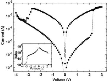
state兲. By sweeping voltage bias to negative over a certain voltage of about −1.7 V, the device is switched from high conductive state to low conductive state共OFF state兲. An abrupt increase in current is present and the device is switched back to ON state again by sweep-ing toward positive voltage bias above a value of about 1.4 V. The typical I-V curve of Ti/Al2O3/Pt device under atmosphere at room temperature is shown in Fig. 2a, and the forming curve is not shown here. Both ON and OFF states are nonvolatile and reversible, quite stable, and the ratio of resistance in both polarities is above three orders of magnitude at low voltage, shown in the inset of Fig. 2a. The bistable memory switching is entirely reversible and reproduc-ible during successive voltage sweeping as shown in Fig. 2b.
The Ti/Al2O3/Pt device exhibits good resistive switching behav-ior and has low forming voltage of about 11 V. It might be attrib-uted to the Ti top electrode extracting a large amount of oxygen ions from the Al2O3film共Al2O3+ Ti→ TiOx+ Al2O3−x兲 and then in-ducing a large amount of oxygen vacancies at the metal-insulator interface共XOo→ XVo
⬙
+ XO2−兲, or modifying the oxygen distribu-tion within Al2O3memory film. As a result, the oxygen content and oxygen-related defects presented in Al2O3films have a great influ-ence on their forming voltage and resistive switching properties.1,3,5 When using Al and Pt as top electrodes in our devices, their forming voltages are so large共over 25 V兲 that they cause permanent damage on the devices, resulting in complete dielectric breakdown. Althoughthe Pt electrode共work function ⬃5.8 eV兲 shows a catalytic adsorp-tion and desorpadsorp-tion effect for oxygen ions, or Al electrode with a similar work function to Ti, their ability of extracting oxygen ions from Al2O3films is worse than that of Ti, leading to higher forming voltages. In Fig. 3 the resistive switching in the Ti/Al2O3/Pt device is also performed at 150°C. However, the resistance ratio, shown in inset of Fig. 3, is obviously lower than that at room temperature, and the ratio of resistance remains 2 orders of magnitude, indicating that the device still can be operated under high temperature. The charac-teristics of ON state under various magnitudes and current compli-ances from 1 to 20 mA were measured and are shown in Fig. 4. The current level of ON state has a linear relation to the compliance current as shown in the inset of Fig. 4. The current values of ON state increase as the current compliances increase, implying the pos-sibility for multibit memory storage.
The I-V characteristics indicated in Fig. 2a were obtained from a typical I-V curve within ±1 V in a double logarithmic plot. Because the slope in the low-field region is very close to 1, the conduction mechanisms of OFF state under low electric field is believed to be satisfied with ohmic conduction. At higher voltage bias, the conduc-tion mechanism of ON state still obeys ohmic conducconduc-tion, implying that ohmic conduction dominates the carrier transport in the ON Figure 2.共a兲 Typical I-V curve of a Ti/Al2O3/Pt structure. Arrows indicate
the sweep direction of the applied dc voltage. The current compliance is set to 5 mA. The inset shows the variation of the resistance ratio with the bias voltage.共b兲 Evolution of ON state and OFF state during sequent voltage sweeping.
Figure 3. Resistive switching phenomenon also can be performed at 150°C with a resistance ratio of two orders of magnitude.
Figure 4. I-V curves obtained by different current compliances. The inset shows the ON state current is in linear relation to value of current compli-ance.
G190 Journal of The Electrochemical Society, 154共9兲 G189-G192 共2007兲
G190
) unless CC License in place (see abstract). ecsdl.org/site/terms_use
address. Redistribution subject to ECS terms of use (see 140.113.38.11
state as shown in Fig. 5a, but it is not suitable for the OFF state. Figure 5b depicts the conduction mechanisms of the OFF state in both positive and negative regions under high electric field as Frenkel-Poole emission by curve fitting. Therefore, the conduction mechanisms dominating in the ON state and OFF state are ohmic
conduction and Frenkel-Poole emission, respectively. The I-V curves of the OFF state are also measured and collected at various temperatures from 30 to 150°C as shown in Fig. 5c. The increasing OFF-state current is observed as the temperature increases. The ac-tivation energy obtained from the slope of the Arrhenius plot as shown in the inset of Fig. 5c is 0.11 eV. Therefore, we believe that the conduction mechanism in the OFF state is Poole-Frenkel emis-sion.
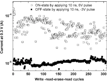
By sweeping dc voltage bias and applying short voltage pulses, both ON state and OFF state can be achieved and are stable over 104s at a read voltage of 0.3 V, as shown in Fig. 6. The EPIR property shown in Fig. 7 is investigated as well, which is important for future nonvolatile memory applications. The asymmetric bipolar switchings are shown in Fig. 6 and 7 in which short pulses applied are 10 ns, 6 V, and 10 ns, and −3 V to switch the device to ON state and OFF state, respectively. In the previous reports, the bipolar resistive switching suggested in Pt/共Ba,Sr兲共Zr,Ti兲O3/Pt might be due to charging and discharging of traps.18Besides, they proposed a model in which the trap can be illustrated as a potential well with different sidewall heights, which might originate from the lattice distortion, tilting, and even the nanopolar regions in paraelectric state. The asymmetrical bipolar resistive switching was also reported
Figure 5. 共a兲 I-V characteristics, obtained from a typical I-V curve within ±1 V, in a double logarithmic plot.共b兲 The conduction mechanisms of OFF state in both positive and negative regions under high electric field are Frenkel-Poole emission by curve fitting.共c兲 The I-V curves of the OFF state measured and collected at various temperatures from 30 to 150°C and the inset shows the Arrhenius plot.
Figure 6. Both ON and OFF state, obtained by dc voltage sweeping and by applying short voltage pulses, stable over 104s at 0.3 V stress.
Figure 7. Write-read-erase-read cycles demonstrated over 300 times by suc-cessively applying a 10 ns, 6 V pulse to switch into ON state and back to OFF state by 10 ns, −3 V pulse.
G191
Journal of The Electrochemical Society, 154共9兲 G189-G192 共2007兲 G191
) unless CC License in place (see abstract). ecsdl.org/site/terms_use
address. Redistribution subject to ECS terms of use (see 140.113.38.11
in Ti/Cu2O/Cu due to the interface reaction that caused asymmetric trap levels to both electrodes.12Based on the above previous works, the asymmetrical bipolar resistive switching in our Ti/Al2O3/Pt de-vice is more likely due to the interface reaction between Ti/Al2O3. Moreover, such a high-speed resistive switching behavior was also demonstrated in the top-electrode/TiON/TiN device,19 the Pt/TiO2/TiN/Pt device,8and a device composed of a Ti layer con-fined by an insulating self-assembly nanogap oxide.20The nanoscle conducting paths are supposed to be formed7 in our Ti/Al2O3/Pt device after the forming process. The resistive switching phenom-enon is believed to occur in certain tiny segments in narrow con-ducting paths while the local Joule heating and electric field are expected to be reinforced in those tiny regions, leading to the high-speed resistive switching.20However, Fujimoto et al. suggested that a nanosecond pulse was quite enough for the sudden increase or decrease of donor concentration by O2−migration in the TiO
2layer of 2.5 nm thickness, which triggered the Mott transition.8The Mott transition cannot be ruled out for the resistive switching phenom-enon. Hence, both the local Joule heating and Mott transition mechanisms might be the reasons for the high-speed resistive switching in our Ti/Al2O3/Pt device. It is going to make the Ti/Al2O3/Pt devices more suitable for NVM applications by modi-fying the device fabrication parameters to improve the ratio of ON/ OFF state resistance and write-read-erase-read cycle number in fu-ture works.
Conclusions
We have demonstrated reproducible and stable resistive switch-ing behavior in a Ti/Al2O3/Pt device. The ratio of resistance of ON and OFF states in both polarities was above 3 orders of magnitude at low voltage. The device also can be operated at 150°C and the resistance value of the ON state can be altered by current compli-ance for possible multibit applications. The dominated conduction mechanisms of both ON state and OFF state are demonstrated as ohmic conduction and Frenkel-Poole emission, respectively. On the basis of our experimental results, which are obtained by dc voltage sweeping and applying short pulse共10 ns + 6 V pulse to switch the device to ON state and 10 ns − 3 V pulse to OFF state兲, both states were stable over 104s and write-read-erase-read cycles were over 100 times. The Ti/Al2O3/Pt devices may be a candidate for further NVM applications.
Acknowledgments
This work was supported by the Taiwan Semiconductor Manu-facturing Company, Limited, and by the National Science Council, Taiwan, under project NSC 95-2212-E-009-120.
National Chiao Tung University assisted in meeting the publication costs of this article.
References
1. A. Sawa, T. Fujii, M. Kawasakai, and Y. Tokura, Appl. Phys. Lett., 85, 4073 共2004兲.
2. C. Y. Liu, P. H. Wu, A. Wang, W. Y. Jang, J. C. Young, K. Y. Chiu, and T. Y. Tseng,
IEEE Electron Device Lett., 26, 351共2005兲.
3. C. C. Lin, B. C. Tu, C. C. Lin, C. H. Lin, and T. Y. Tseng, IEEE Electron Device
Lett., 27, 725共2006兲.
4. L. P. Ma, S. M. Pyo, Q. F. Xu, and Y. Yang, Appl. Phys. Lett., 82, 1419共2003兲. 5. S. Seo, M. J. Lee, D. H. Seo, E. J. Jeoung, D.-S. Suh, Y. S. Joung, I. K. Yoo, I. R.
Hwang, S. H. Kim, I. S. Byun, I.-S. Kim, J. S. Choi, and B. H. Park, Appl. Phys.
Lett., 85, 5655共2004兲.
6. D. C. Kim, S. Seo, S. E. Ahn, D.-S. Suh, M. J. Lee, B.-H. Park, I. K. Yoo, I. G. Baek, H.-J. Kim, E. K. Yim, et al., Appl. Phys. Lett., 88, 202102共2006兲. 7. K. Kinoshita, T. Tamura, M. Aoki, Y. Sugiyama, and H. Tanaka, Appl. Phys. Lett.,
89, 103509共2006兲.
8. M. Fujimoto, H. Koyama, M. Konagai, Y. Hosoi, K. Ishihara, S. Ohnishi, and N. Awaya, Appl. Phys. Lett., 89, 223509共2006兲.
9. I. G. Baek, M. S. Lee, S. Seo, M. J. Lee, D. H. Seo, D.-S. Suh, J. C. Park, S. O. Park, H. S. Kim, I. K. Yoo, et al., Tech. Dig. - Int. Electron Devices Meet., 2004, 587.
10. D. Lee, H. Choi, H. Sim, D. Choi, H. Hwang, M.-J. Lee, S.-A. Seo, and I. K. Yoo,
IEEE Electron Device Lett., 26, 719共2005兲.
11. H. Sim, D. Choi, D. Lee, S. Seo, M.-J. Lee, I. K. Yoo, and H. Hwang, IEEE
Electron Device Lett., 26, 292共2005兲.
12. T.-N. Fang, S. Kaza, S. Haddad, A. Chen, Y.-C. Wu, Z. Lan, S. Avanzino, D. Liao, C. Gopalan, S. Choi, et al., Tech. Dig. - Int. Electron Devices Meet., 2006, 789. 13. T. W. Hickmott, J. Appl. Phys., 33, 2669共1962兲.
14. T. W. Hickmott, J. Appl. Phys., 34, 1569共1963兲. 15. T. W. Hickmott, J. Appl. Phys., 35, 2118共1964兲.
16. O. Kurnosilkov, F. C. de Nooij, P. LeClair, J. T. Kohlhepp, B. Koopmans, H. J. M. Swagten, and W. J. M. de Jonge, Phys. Rev. B, 64, 153407共2001兲.
17. K. M. Kim, B. J. Choi, B. W. Koo, S. Choi, D. S. Jeong, and C. S. Hwang,
Electrochem. Solid-State Lett., 9, G343共2006兲.
18. Y. Xia, W. He, L. Chen, X. Meng, and Z. Liu, Appl. Phys. Lett., 90, 022907 共2007兲.
19. T. Hosio, Y. Tamai, T. Ohnishi, K. Ishihara, T. Shibuya, Y. Inoue, S. Yamazaki, T. Nakano, S. Ohnishi, N. Awaya, et al., Tech. Dig. - Int. Electron Devices Meet.,
2006, 793.
20. Y. Ogimoto,Y. Tamai, M. Kawasaki, and Y. Tokura, Appl. Phys. Lett., 90, 143515 共2007兲.
G192 Journal of The Electrochemical Society, 154共9兲 G189-G192 共2007兲
G192
) unless CC License in place (see abstract). ecsdl.org/site/terms_use
address. Redistribution subject to ECS terms of use (see 140.113.38.11