國 立 交 通 大 學
電機學院光電顯示科技產業研發碩士班
碩 士 論 文
配向層表面極性對 FLC 排列之影響
Alignment Layer Polarity Effects on Ferroelectric
Liquid Crystals
研 究 生 : 黃耀慶
指 導 教 授 : 陳皇銘
配向層表面極性對 FLC 排列之影響
Alignment Layer Polarity Effects on Ferroelectric Liquid
Crystals
研 究 生 : 黃耀慶
Student : Yao-Ching Huang
指 導 教 授 : 陳 皇 銘
Advisor : Huang-Ming Philip Chen
國 立 交 通 大 學
電機學院光電顯示科技產業研發碩士班
碩 士 論 文
A Thesis
Submitted to College of Electrical and Computer Engineering National Chiao Tung University
in partial Fulfillment of the Requirements for the Degree of
Master in
Industrial Technology R & D Master Program on Photonics and Display Technologies
July 2007
Hsinchu, Taiwan, Republic of China.
i
配向層表面極性對鐵電性液晶排列之影響
研究生: 黃耀慶 指導教授: 陳皇銘 博士
電機學院光電顯示科技產業研發碩士班
摘要
鐵電型液晶具有快速反應的特性,使得其成為下一世代高品質顯示器的候選人之一。 然而不易達成良好排列特性阻礙了在商業上的量產。在本文中,我們從基本原理上來探 討表面穩定鐵電型液晶的主要排列缺陷之一形成的原因和解決方案:Horizontal Defect。 我們提出利用上下層具有不同極性的配向材料,將能有效的消除 Horizontal Defect;因此 HMDS 和 Nylon 6 兩種具有正極性材料以及 PI 具有負極性的材料使用來做 成 Hybrid Cell 。 從 結 果 中 發 現 此 兩 種 配 向 材 料 在 鐵 電 性 液 晶 中 可 以 成 功 壓 抑 Horizontal Defect 形成,使得整體排列缺陷減少,進而提高顯示器對比,解決鐵電型 液晶排列的問題。ii
Alignment Layer Polarity Effects on
Ferroelectric Liquid Crystals
Student: Yao-Ching Huang Advisor: Dr. Huang-Ming Philip Chen
Display Institute
National Chiao Tung University
Abstract
A method solving horizontal defect of FLCs was proposed based on elastic-continuum theory. According to the theory, FLCs of the uniform state in the cell had two stable states (azimuthal angle φ=0 or π) which possessed the same minimum free energy and horizontal defect would always appear. Only one stable state had the minimum free energy so that horizontal defect no more observed in the cell, by using hybrid cell configurations which adopted two different alignment layers with opposite polarity,
Our results showed that horizontal defect-free state was successfully achieved by using three different kinds of hybrid cells. Our breakthrough produced satisfied dark state, solved the alignment problem of FLCs and made FLCs application in displays become hopeful.
誌謝
本篇論文能夠完成,首先要感謝的是在這兩年中,給予我殷殷教誨的指導教 授陳皇銘老師,老師的豐富學識以及對學術探索精神,使我能在科學研究上受益 良多,而在做人處事上,老師風範也讓我體會一位學者該有的研究態度與要求, 我期勉未來自己能秉持老師的指導,在未來開創自己的人生。 其次我要感謝是友達光電願意支持我就讀於交通大學顯示光電產專,在經費 上予以協助,使我得以減輕經濟的負擔。 再來我要感謝實驗室的學長淇文、昀諺、世民和宜揚在實驗上的指導,讓我 的實驗得以順利進行,若沒有他們過去經驗傳承,我的研究並沒有辦法順利進行。 此外,我也要感謝實驗室的同學,沒有你們的鼓勵以及在多少個深夜與凌晨陪伴, 我將無法持續下去完成我的實驗;而在實驗遭遇挫折時,也多虧有你們的幫助, 我才能順利找到解決方法,感謝威慶、耿睿、昆展、佳恬、俊民、佑儒、鴻杰你 們的協助;另外,學弟謹瑋在過去一年給予的協助,也是我深深感激的。 最後,感謝在背後一直默默支持我的家人們,因為有你們的陪伴與鼓勵,讓 我能夠堅持下去,完成學業,成功的邁向未來旅程。 在此,謹將這份喜悅分享與所有關心我的人,這份恩情我將會永遠銘記在心! iiiiv
Table of contents
Chinese abstract ……….. i English abstract ………... ii Acknowledgement ………... iii Table of contents ……….………... iv List of Figures ……… vi List of Tables ……… ixChapter 1 Introduction and Background 1.1 Liquid Crystal displays Market and Technology ……….. 1
1.2 Liquid Crystals ……..………. 2
1.2.1 Liquid Crystal Phases………. 3
1.3 Ferroelectric Liquid Crystal Displays (FLCDs)………. 8
1.4 Motivation and Objectives……...………...…………... 9
1.5 Contents of This Thesis……..……… 9
Chapter 2 Literature Review 2.1 SSFLC Structure ………... 10
2.2 Zigzag Defect in SSFLC………. 11
2.2.1 Chevron Structure and Zigzag Defect………... 11
2.2.2 Methods to Erase Zigzag Defect……….. 15
2.3 Horizontal Defect in SSFLC………...……….……... 17
Chapter 3 Measurement Instruments and Cells Fabrication Process 3.1 Measurement Systems………..………. 24
3.1.1 Introduction………..……… 24
3.1.2 Atomic Force Microscope (AFM)…..……….. 24
3.1.3 Cell Gap Measurement System………. 27
3.2 Cells Fabrication………...……….. 30
Chapter 4 Experiment Results 4.1 Polarity Test…...………. 33
v
4.2 Hybrid Cell………..………… 37
4.2.1 HMDS Hybrid Cell Test………...………. 37
4.2.2 Nylon 6 Hybrid Cell Test………...………... 39
Chapter 5 Conclusions
5.1 Summary………... 42
5.2 Future Work……… 43
vi
List of Figures
Figure 1-1. Phase and molecular order for crystalline solid, liquid crystal, and liquid... 3 Figure 1-2. (a) Nematic phase with high orientational order but lower positional order
(b) Smectic Phase with high orientational and positional order……… 4
Figure 1-3. Molecules arranged in (a) Smectic A phase and (b) Smectic C phase……….. 5 Figure 1-4.Chiral nematic A liquid crystal and selective reflection principle. The nematic
molecules only make a π radians rotation along the helix axis and the pitch is p/2………... 6
Figure 1-5. The helix in a layer structure of the SmC* liquid crystal……….. 7 Figure 1-6. Operation principle of a SSFLC switching. The applied field switched the
structure between two stable states, resulting in (a) a dark state and (b) a bright state………. 8
Figure 2-1.Two stable states in surface stabilized FLC configuration SSFLC). The
helical structure was unwound by the surface action and both molecular states are equally stable………. 11
Figure 2-2. Bookshelf structure of (a) SmA and (b) ideal transition from SmA to SmC or
SmC*………. 12
Figure 2-3. C1 and C2 bookshelf structure……….. 13 Figure 2-4. (A) The upper figure showed the chevron structure of C1 and C2 states, and
the lower one showed the shape of zigzag. (B) Picture of zigzag defects under POM……….... 13
Figure 2-5.Schematic illustration of the geometrical conditions for C1, C2 states. α, θc,
and δ are pretilt angle, cone angle, and layer tilt angle………. 14
Figure 2-6.Schematic illustration of the horizontal defects, as a top view of the cell, in
the SSFLC………. 17
Figure 2-7.Microscopic textures of multi-domain cell when an electric field was applied.
Area B only responds to negative field while area A only responded to a
vii
Figure 2-8.Illustration of coordinate system. θ was the cone angle, φ was the azimuthal
angle of the cˆ director, and the nˆ was molecular director…….. 19
Figure 2-9. (a) The coordinate system of FLC molecules in the cell. (b) FLC molecules
aligned in a uniform stable state with the minimum energy at Φ=0. (c) FLC molecules aligned in the other uniform stable state with the same minimum energy at Φ=π……… 22
Figure 3-1. Concepts of AFM and the optical lever………. 25 Figure 3-2. Two reflecting surfaces separated by a layer causing a light interference. The
dotted line indicated the first internal reflection……… 27
Figure 3-3. The reflection as a function of wavelength using an air gap of 5.0μm……….. 29 Figure 3-4. Experiment process of cells fabrication………. 30 Figure 4-1. Sign of surface polarity and the direction of the dipole moment……….. 34 Figure 4-2.The relationship between layer direction and the polarity direction of the
alignment layers in twisted FLC mode when the sign of the spontaneous polarization was negative……….. 35
Figure 4-3. Pictures of the cross-rubbing cells taken by POM. Pictures at the right were
the magnified layer structures. (a) Layer structure in PI cell. (b)Layer structure in PVA cell………. 36
Figure 4-4. Pictures of the cross-rubbing cells taken by POM. Pictures at the right ware
the magnified layer structures. (a) Layer structure in PI cell. (b)Layer structure in Nylon 6 cell……….... 36
Figure 4-5. (a) HMDS hybrid cell injected with R2301. (b) HMDS hybrid cell injected
with 50% R3206. (c) Cell with only one side coated with PI and injected with 50% R3206……… 37
viii
Figure 4-6. Normally white TN configuration of (a) PI alignment layer. (b) HMDS
alignment layer baked at 90 for 0.5 hour. (c) HMDS alignment layer ℃
baked at 110 for 0.5 hour………..℃ 38
Figure 4-7. Nylon 6 hybrid cells with single rubbing (a) 50% R3206 (b) R2301………… 39 Figure 4-8. (a) The cell coated with Nylon 6 on both sides and injected with 50% R3206.
(b) (a) The cell coated with PVA on both sides and injected with 50% R3206. (c) and (d) are hybrid cells coated with Nylon 6 and PI……….………. 40
Figure 4-9. (a) The cell coated with Nylon 6 on both sides and injected with R2301. (b)
The cell coated with PVA on both sides and injected with R2301.
ix
List of Tables
Table 3-1. Coating parameters and baking temperatures for PI (polyimide, Chisso
PIA-X201-G01), PVA (polyvinylalchol), HMDS (Hexamethyldisilazane), and Nylon 6. Nylon 6 was baked and rubbed twice……… 31
Table 3-2. Rubbing parameters of alignment materials. Pile impression meant the gap
between the substrate and the roller……… 31
Table 4-1. The sign of the polarity of different alignment layer………...
1
Chapter 1
Introduction and Background
1.1 Liquid Crystal Displays Market and Technology
Liquid crystal displays (LCDs) play an important role in the development of flat panel displays (FPDs) which are essential components in information electronics products today. Compared with the cathode ray tube (CRT) used in traditional televisions, LCDs are thin, lightweight, and power efficient devices that present images with high quality performance. As a result, LCDs represent a large and rapidly growing industry worldwide, and are expanding into an increasingly diverse set of systems. Liquid crystal displays are used everywhere. The small applications include portable devices, such as portable DVD players, mobile phones, digital cameras, handheld games, pictures viewers and many others, which did not even exist a few years ago. And there appears to be no end to the applications requiring small sized displays. In the area of large screens (Active Matrix AM or Thin Film Transistor TFT technology), liquid crystals fit into all branches including video, TV and HDTV applications along with high resolution laptop screens and desktop monitors.
Today’s TFT-LCD market is dominated by the nematic technology. Mainly two types of panels significantly penetrated the market: VA-LCD (Vertically Aligned) and IPS-LCD (In Plane Switching) which achieve high contrast ration and enhance viewing angle fitting well into today’s requests. Future displays, however, based on new device concepts (e.g. Field Sequential Display FSD), have much higher requirements, for
2
which nematic liquid crystals inherently limit of response speed are not appropriate.
In addition to nematic materials, smectic liquid crystals play a special role in LCD’s because of an intrinsic fast response in the microsecond range which is easily 1000 times faster than that of nematic liquid crystals. Unfortunately, manufacturing smectic based devices is very challenging since it requires a small cell gap less than 2 micrometers. Although smectic materials look promising from a material point of view, unreliable production, and lower contrast ratio are important issues. Therefore, improving contrast ration is the main subject of this thesis.
1.2 Liquid Crystals
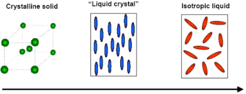
Liquid crystals (LCs) possess characteristics of fluidity, observed in liquids, but anisotropic physical properties, observed in crystalline states. They represent thermodynamically stable phases situated between isotropic liquids and the crystalline solids, as shown in Figure 1-1. The liquid crystal phase, also known as the mesophase, can be further subdivided into several various phases, depending on the amount of order they possess. There are two main liquid crystal phases: the nematic phase which exhibits orientational order and no positional order and the smectic phase, which exhibits both orientational and partial positional order [1].
3
Figure 1-1. Phases and molecular order for crystalline solid, liquid crystal, and
liquid.
1.2.1 Liquid Crystal Phases
Nematic A Phase
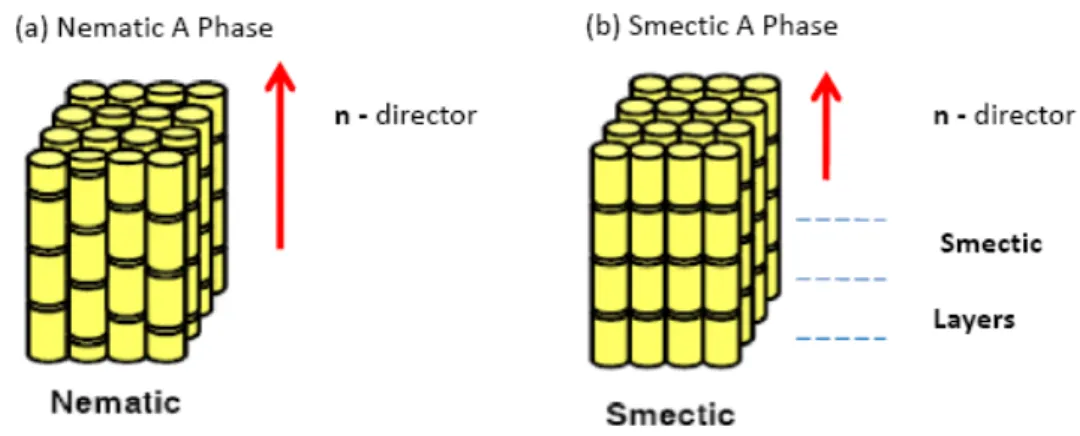
In the Nematic A phase (See Figure 1-2a), a unit vector n, named director, is used to represent the long axes direction of molecules. Liquid crystal molecules are averagely aligned and parallel to n which represents the direction of the optic axis of the system. The nematic phase possesses an orientational order. Only the long axis of the molecules is more or less oriented, but there is a random distribution between the heads and the tails of the molecules. As a result, the nematic phase is optically uniaxial. The measure of the degree of order in nematic phase is given by the so-called order parameter:
,where ω is the deviation angle of each molecule from the director. If S=0, the substance is in isotropic phase (randomly ordered); S=1, the substance is in solid state (perfectly ordered). Typically, liquid crystal has 0.5<S<0.7.
(1.1) 2 1 cos 2 3 2 − 〉−−−−−−−−−− 〈 = ω S
4
Smectic A phase
In Smectic A (SmA) phase, molecules’ position is ordered in layers except for having orientational order. The layer spacing is approximately equal to the length of the molecules as shown in Figure 1-2b. We call this as positional order and the director in the SmA phase is normal to the smectic layers and determines the optic axis of the system. Motion of molecules is restricted within these layers, and adjacent layers are observed to flow past each other. To the conclusions, molecules in SmA phase are much ordered than those in Nematic A phase and optically uniaxial which is similar to Nematic A phase.
Figure 1-2. (a) Nematic phase with high orientational order but lower positional
5
Smectic C Phase
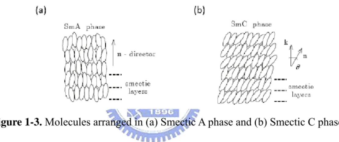
In Smectic C phase, molecules are arranged like Smectic A phase but the lone axes are tilted in a preferred direction with respect to the layer normal (see Figure 1-3). The tilt direction of the molecules in neighboring layers is correlated and it is denoted by a unit vector c, called c-director. The angle between the director and the layer normal k defines the tilt angle of the material and is denoted as θ. The plane in which the tilt angle is defined, thus the plane spanned by k and n is usually called tilt plane.
6
Chiral Nematic A phase – N*
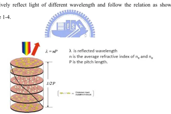
If we mix a chiral dopant with a nematic liquid crystal, a nematic phase with twisted structure known as chiral nematic N* (or cholesteric) is formed (Figure 1-4). As a result the director in the N* phase, instead of being uniformly oriented, rotates in space about an axis that is perpendicular to it. Macroscopically the helical superstructure develops with a twist axis perpendicular to the local director. If the director makes a full 2π radians rotation along the helix axis, the distance needed to form the rotation is called helical pitch P. The pitch strongly depends on the concentration of the dopant in the mixture and varies typically between a few hundred nanometers to many micrometers. In additions, the helical structure of N* phase can selectively reflect light of different wavelength and follow the relation as shown in Figure 1-4.
Figure 1-4. Chiral nematic A liquid crystal and selective reflection principle. The nematic molecules only make a π radians rotation along the helix axis and the pitch is p/2.
7
Chiral Smectic C Phase – SmC*
Just like N*, chiral smectic C (SmC*) can be formed if chiral dopants are mixed with achiral molecules in smectic C phase. When the molecules of mixture become chiral, successive smectic C layer shows a gradual change in the direction of tilt, so that the director rotates around the z-axis from layer to layer. Besides, chirality also induces the spontaneous polarization and the spontaneous polarization is tangent to the smectic
cone and the director. What causes the chirality is the symmetry degrading from C2h in
SmC to C2 in SmC* [2]. The distance that the director rotates 2π radians along the
smectic cone is called a pitch. Figure 1-5 illustrates the basic structure of SmC*.
8
1.3 Ferroelectric Liquid Crystal Displays (FLCDs)
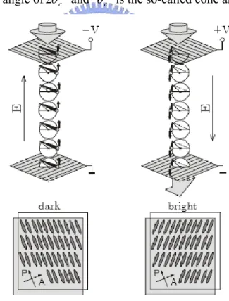
Clark and Langerwall (1980) proposed the SSFLC structure and this type was the mainstream of FLC displays. In SSFLC device, the FLC was sandwiched between two closely spaced solid substrates (d << 1 pitch). In this configuration, the helix structure is unwound and molecules align along the rubbing direction. As shown in Figure 1-6, two stable states existed and the dark state is got when the director of one stable state was set to be parallel to the polarizer and the analyzer is crossed with the polarizer. When electric field is applied, the polarization Ps aligns with along the electric field E and the molecules will change so that the bright state appeared. These two stable states differ from an azimuthal angle of2 and θc θc is the so-called cone angle.
Figure 1-6. Operation principle of a SSFLC switching. The applied field switches
the structure between two stable states, resulting in (a) a dark state and (b) a bright state.
9
The SSFLCs have many technical advantages: the switching time is very short (in sub-millisecond range) due to the direct coupling between the Ps and an electric field. An analog gray scale is possible by utilizing a small Ps material. The in-plane like switching provides a naturally wide viewing angle. However, the main challenge of FLC devices is the alignment defect, such as zigzag defect and horizontal chevrons, which causes light leakage and degrades the contrast ratio.
1.4 Motivations and Objectives
FLC has the potential application in future field-sequential-display, but the defects hindered the commercialization development. How to get a good mono-domain and defect-free alignment are very important issues. In our study, we want to discuss what causes the defects to occur and the methods to solve the problem so that real commercialized FLCS displays can enter into the market, soon.
1.5 Contents of This Thesis
In following sections, two major defects, zigzag defects and methods to solve them would be discussed and introduced in Chapter 2. Chapter 3 describes the measurement systems and cells fabrication process adopted in this thesis. The experimental results and discussions are presented in chapter 4. Chapter points out the conclusions and future work.
10
Chapter 2
Literature Review
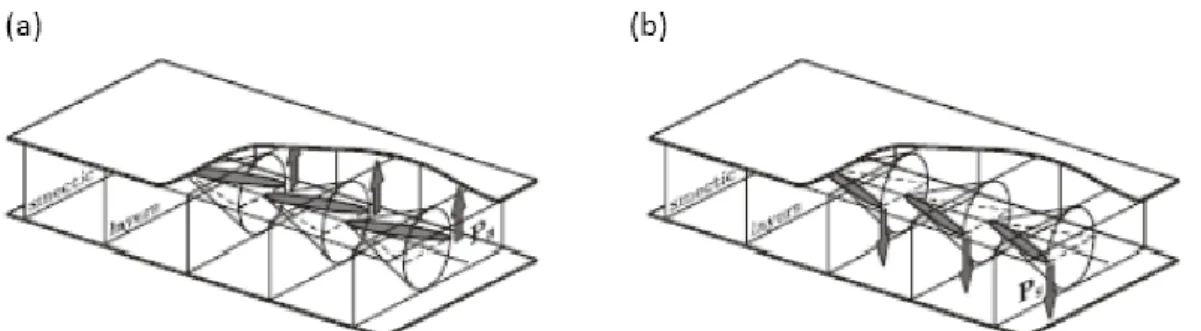
2.1 SSFLC Structure
In 1980 Clark and Lagerwall [3, 4] proposed a new device structure which can unwind the helix of a SmC* material if the cell gap between two plates was much smaller than the helical pitch ( << 1 pitch), as shown in Figure 2-1. In addition to having sub-microsecond switching, two symmetric stable states existed so that the device was
bistable. The spontaneous polarization vector, Ps, was tangential to the molecule and
perpendicular to the alignment surface. Molecules of two stable states aligned in
different direction accompanying with upward and downward Ps, respectively. We
called this as surface stabilized ferroelectric liquid crystals (SSFLC).
Besides, the LC molecules motion under applied electric field was similar to in-plane-switching mode (IPS mode) so that SSFLCs had wide viewing angle merit. Fast response time and wide viewing angle characteristics were suitable for field sequential displays, which attracted many researchers. Although SSFLC had superior advantages in field sequential displays, its inherent poor alignment causes serious light leakage and hindered the commercialization development. In this section, the reasons and theories of poor alignment would be reviewed. Also solving method would be proposed from theories.
11
Figure 2-1. Two stable states in surface stabilized FLC configuration SSFLC). The
helical structure was unwound by the surface action and both molecular states are equally stable.
2.2 Zigzag Defect in SSFLC
Achieving satisfying alignment in SSFLC was a very difficult task because of two dominant defects, zigzag defect and horizontal defect. The former was from chevron structure formation of SmC* in SSFLC configuration while the latter was from that two stable states had the same minimum energy. These alignment problems and possible solutions would be reviewed step by step in this section.
2.2.1 Chevron Structure and Zigzag Defect
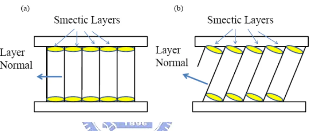
Zigzag defect was often appeared in SSFLC cells, causing serious light leakage that lowers the contrast ratio. What causes the defect was the formation of chevron structure in SSFLC. The origin of chevron layer formation, found by X-ray measurements from Rieker [5], was explained by discrepancy between the layer spacing of the SmC* phase and SmA phase. In smectic A phase, the LC molecules aligned along the rubbing direction and form the parallel bookshelf structure, as shown in Figure 2-2.
12
When the homogeneous aligning cell cooled down from SmA phase to SmC* phase, the molecules tended to tilt an angle. The layer spacing between the two substrates would shrink from dA to dC but the layer spacing still fixed at dA. Thus the layer was tilted from the top and the bottom substrates and the relation between dA and
dC was shown as equation (2-1).
, where δC was the layer tilted angle in SmC* phase.
Figure 2-2. Bookshelf structure of (a) SmA and (b) ideal transition from SmA to
SmC or SmC*
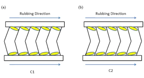
But the situation mentioned above was ideal. In reality, the molecules at the top and bottom substrates would tilt differently so that the chevron structure appeared, as shown in Figure 2-3. There were two different chevron structures, named C1 and C2, existing in SSFLC cells [6]. If the tilting direction of chevron was toward to the rubbing direction, we called this as the C2 state. On the contrary, if the tilting direction of chevron was opposite to the rubbing direction, it was the C1 state.
1) --(2 -cos C A C d d = δ
13
Figure 2-3. C1 and C2 bookshelf structure
These two chevron structures often coexisted in SSFLC cells and the zigzag defect was caused by discontinues in the chevron layer structures, as shown in Figure 2-4. The C1 and C2 states were easily distinguished because the tilting direction of the chevron layer structure, confirmed by the direction of the zigzag defect [7] and the rubbing direction surface pretilt was consistent with the rubbing direction [8].
Figure 2-4. (A) The upper figure showed the chevron structure of C1 and C2
states, and the lower one showed the shape of zigzag. (B) Picture of zigzag defects under POM.
14
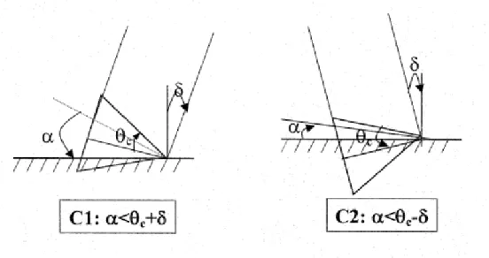
Kanbe [9] found the essential criteria to fulfill of the formation of C1, C2 states substructure, as shown in Figure 2-5. At lower pretilt angle alignment layer, C1 and C2 states could exist at the same time. However, at higher pretilt angle alignment layer, only C1 state could survive because the director cannot lie on the switching cone in C2 state. Based on this criteria, if at high temperature just below the transition temperature between SmA and SmC*, C1 state appeared only because the cone angle and layer tilt
angle were still very small. Upon cooling down to lower temperature, θc−δ increased
gradually and the transition from C1 to C2 state started. Finally, C1 state and C2 state coexisted in the cell and form the zigzag defects.
Figure 2-5. Schematic illustration of the geometrical conditions for C1, C2 states. α,
15
2.2.2 Methods to Erase Zigzag Defect
There were three methods to get no zigzag defect cells. The first two methods were to get C1 or C2 uniform orientation only within one cell. Kanbe et al. [9] reported that a combination of the high pretilt aligning film and a low tilt angle for the FLC material was required to obtain the C1U state and prevented the appearance of the C2 state. In the application of display, Koden et al. [10] and Tsuboyama et al. [11] showed good display performance with a uniform C1U orientation by using a high pretilt alignment layer with a low tilt FLC material.
About C2 uniform orientation, two useful approaches to realize the formation of a C2U orientation had been reported. One approach involved an investigation of the method of alignment. The C2 orientation was possible in the low pretilt angle condition, but it was impossible in the high pretilt angle condition [12]. Strong rubbing had also been reported as being favorable to producing the C2 orientation [13] because the direction of molecules on a surface in the C2 orientation became almost the same as the direction of rubbing and that was insensitive to variations in alignment, surface polarity, memory effects, and surface switching. The other approach was to investigate the relationship between the properties of materials and the formation of C2 orientation. To obtain the C2 orientation, a material must be in the SmA phase over a wide range of temperatures [13]. This was because the FLC materials were in SmA phase over a wide range of temperature tended to have small tilt angles near the SmC to SmA transition point. This small tilt angle could reduce the energy barrier for transition from the C1 to the C2 state near the SmC to SmA transition point because the small tilt angle leaded to chevron layers leaning at a small angle. Besides, Furue et al. adopted polymer-stabilized method to obtain defect free C2U orientation [14].
16
The last approach to get zigzag defect was quasi-bookshelf structure. Three major approaches had been investigated to obtain a bookshelf layer structure. First approach was AC-field treatment [15]. An initial chevron layer structure is turned into a bookshelf layer structure by applying a strong low frequency AC field. High Ps of FLC material was required because the interaction between the electric field and Ps induces a torque that changed the layer structure from chevron to bookshelf.
Second approach was utilizing a unique class of materials with tilt angles that were weakly dependent on temperature. In the previous section, the chevron layer structure was the reduction of layer spacing brought about by cooling. The reduction of layer spacing was usually observed in FLC materials with an INAC (Iso – N – A – C) phase sequence; because the tilt angles of such FLC materials were usually strongly dependent on temperatures. However, there was unique of FLC materials with an INC (Iso – N – C) phase sequence which the tilt angles were weakly dependent on temperature [16]. It was possible to realize a bookshelf layer structure without electrical field.
Third approach utilized FLC materials with an INC phase sequence, and the DC voltage applied during the material cooled and changed from the N to SmC phase. The quasi-bookshelf orientation was suitable for active matrix drive method, because it exhibited mono-stable and a smooth V-T characteristic. This mode was called CDR (continuous director rotation) or Half-V shaped FLC [17-18].
17
2.3 Horizontal Defect in SSFLC
In common LCD production, the rubbing process was often adopted to align the liquid crystal molecules so that the LC molecules would fix at the surface of alignment layer and force the bulk LC to orient toward rubbing direction. In SSFLC, molecules would also align along the rubbing direction but lie on two different cones so that a folding of smectic layer took place, as shown in Figure 2-7. Multi-domains were forming with spontaneous polarization pointing upward or downward into the substrate. The reason why two kinds of directors were generated was explained as following. When the cell entered the SmC* phase, two directions of smectic layers were formed and tilted respect to the rubbing direction.
Figure 2-6. Schematic illustration of the horizontal defects, as a top view of the cell,
in the SSFLC.
When an electric filed was applied to the cell with multi-domain, the adjacent domains switched in different ways [19], as shown in Figure 2-8. The type A domain
18
only responding to a positive field turned to the bright state when a positive voltage was applied. On the other hand, when a negative voltage was applied, only the type B domain switched to bright. Multi-domains resulted in light leakage and reduced the contrast ratio.
Figure 2-7. Microscopic textures of multi-domain cell when an electric field was
applied. Area B only responded to negative field while area A only responded to a positive electric filed.
What caused the horizontal defect could be conducted from Chieu [20] calculation of elastic-continuum theory. In elastic-continuum theory, the elastic distortion free energy density of a SmC* materials would be written in the Oseen-Frank form, as shown in equation 2-1. bend. s spontaneou of vector wave the is twist. s spontaneou of vector wave the is director. the is ly. respective constants, elastic bend and twist, splay, the are and , , Where 1) --(2 -2 2 2 3 2 1 2 3 2 2 2 1 b t ^ b ^ ^ t ^ ^ ^ d q q n K K K ) q n rot n ) ( / +(K ) -q n rot n )( / +(K ) n ) (div / = (K W • × −
19
Figure 2-8. Illustration of coordinate system. θ is the cone angle, φ is the
azimuthal angle of the cˆ director, and the nˆ is molecular director.
As shown in Figure 2-9, the nˆ director is expressed equation 2-2.
The wave vectors q and t q were given by b
Where qo = 2π / p, p was the pitch length, and the sign of q specifies the o
handedness of the LC helicoids.
Under the condition of constant cone angle, the simplest surface-stabilized structures were those where the variation of φ is restricted to the y direction normal to the bounding surfaces. The elastic distortion energy density could be expressed as
Where φy was the partial derivative of φ with respect to y axis. 2) --(2 -cos sin sin cos sinθ , θ , θ) ( n^ = φ φ 4) --(2 -cos 3) --(2 -sin 0 2 0 ) z n θ( q q θ q q ^ ^ b t × = − = 5) --(2 -cos sin sin 2 sin cos sin sin sin cos cos sin 2 2 3 2 2 2 2 0 3 3 2 0 2 2 3 2 2 2 1 2 2 θ) K θ θ(K ) / (q θ θ ) K (K q ] θ) K θ (K θ[K ) ( W y y d + + − + + + = φ φ φ φ φ
20
The surface energy per unit area arising from the molecular interactions with the bounding surfaces was given by
Where the summation summed the contributions from both top and bottom surfaces ( i = t, b), sˆ, pˆwere the unit vectors of the surface normal and the polarization, and ()
1 i r and () 2 i
r were the non-polar and polar surface-interaction coefficients, respectively.
Keeping the lowest order terms, it could be expressed as
Where φt and φb were azimuthal angles at the upper surface y = d / 2 and at the
lower surface y = -d / 2, and d was the thickness of the cell. The total free energy per unit area was thus given by
To minimize the total free energy to obtain the surface-stabilized states, we solved the Euler-Lagrange equation,
, and the surface torque-balance equations,
, and
Where φyy was the second derivative of φ with respect to y. 6) --(2 -] ˆ ˆ ˆ ˆ [r1 (n s) r2 (p s) F (i) i (i) s =
∑
• + • 7) --(2 -cos cos sin sin sin 2 2 2 1 2 1 2 b (b) t (t) b (b) t (t) s θ(γ γ ) r γ F = φ + φ − φ + φ 8) --(2 -2 2 s d/ d/ Wddy F F =∫
+ − 9) --(2 -0 2 sin )] sin cos ( [ 2 1 ] sin sin cos cos [ 2 3 2 2 1 2 2 2 3 2 2 2 1 = + − − + + φ φ φ φ φ θ K θ K K θ) K θ (K K y (t) yy 10) --(2 -0 sin ] cos sin ) ( [ 2 sin sin ] sin ) sin cos ( cos [ sin t ) ( 2 3 3 2 2 ) ( 1 2 2 3 2 2 2 1 2 ) ( = + − + + + + φ θ θ φ θ φ θ θ φ θ φ t o t t t t t y r K K q r K K K 11) --(2 -0 sin ] cos sin ) ( [ 2 sin sin ] sin ) sin cos ( cos [ sin ) ( 2 3 3 2 2 ) ( 1 2 2 3 2 2 2 1 2 ) ( = + − + + + + b b o b b b b b y r K K q r K K K φ θ θ φ θ φ θ θ φ θ φ21
The orientation structures were given by solutions from equation 2-9 to 2-11 including three non-equal elastic constants. The simplest solution was φy =0 or
.
const
=
φ , which gave the uniform up (φt =φb =0) and down (φt =φb =π ) state.
After complicated calculation, Chieu proposed FLC molecules within the cell have three different states: uniform, splayed, and helical state. Each state had different total distortion energy per unit area and could be represented as equation 2-12, 2-13, and 2-14, respectively.
z Uniform State:
Where the – and + signs corresponded to up and down states, respectively.
z Splay State: z Helical State: 12) --(2 -) ( ) cos sin ( sin 2 ) ( 2 ) ( 2 2 3 2 2 2 2 0 t b u K K r r dq F = θ θ + θ m − 12) --(2 -cos cos ) sin sin ( sin ) cos (cos cos sin ) ( ) cos sin ( sin 2 sin 2 ) ( 2 ) ( 2 2 ) ( 1 2 ) ( 1 2 3 3 2 2 3 2 2 2 2 2 b b t t b b t t b t o o spl r r r r K K q K K dq C d F φ φ φ φ θ φ φ θ θ θ θ θ θ + − + + − − − + + = 13) --(2 -sin ) ( 2 1 ( ) 2 1 ) ( 1 θ b t u r r F = −
22
For getting ideal alignment, FLC molecules within the cell must be kept in the uniform state. And the parameters which affected were the critical cell thickness, cone angle, the helical pitch, the elastic constants of FLC materials, and the surface interaction between substrates and liquid crystals.
However, even if the proper parameters were taken to make the FLC molecules stay in uniform state, horizontal defect would not be erased because two stable states in the uniform type had the same minimum energy, as shown in Figure 2-10. In equation
2-12, γ2 is the polar surface-interaction coefficient and was related to the surface
alignment layer polarity. Therefore, if the alignment layers were the same for top and bottom substrates, FLC molecules would align along the rubbing direction with its polarization direction upward or downward into the substrates which caused the horizontal defect to occur.
Figure 2-9. (a) The coordinate system of FLC molecules in the cell. (b) FLC
molecules aligned in a uniform stable state with the minimum energy at Φ=0. (c) FLC molecules aligned in the other uniform stable state with the same minimum energy at Φ=π.
23
Some methods were proposed to solve horizontal defect, too. A DC voltage applied to the liquid crystal only near the transition temperature from N* to SmC* phase to form one type of domain with the Ps in either upward or downward direction had been proposed [21]. However, by applying the DC voltage for more than several minutes, residual charge generated in the cell, which may reduce the contrast of LCD. Applying the AC field was another way to eliminate the horizontal defect, a triangular wave [22],
square wave [23], or asymmetric rectangular waveform [24]was used.
In our study, a new concept without applying an electric field would be proposed from equation 2-12 conduction. This will be explained gradually in the upcoming chapter.
24
Chapter 3
Measurement Instruments and Cells Fabrication
Process
3.1 Measurement Systems
3.1.1 Introduction
In this chapter, the measurement setups used in the experiments were described in the following sections. The surface morphology was inspected by AFM. After making an empty cell, the cell gap was measured by interferometric method, which was described in detail in section 3.1.2.
3.1.2 Atomic Force Microscope (AFM)
AFM had a number of advantages that it provided easily achievable high-resolution and three-dimensional information in real space with little sample preparation for low-cost. It consisted of a scanning sharp tip at the end of a flexible cantilever across a sample surface while maintaining a small, constant force. The tip typically had an end radius of 2 nm to 20 nm, depending on its type. The scanning motion is conducted by a piezoelectric tube scanner which scans the tip in a raster pattern with respect to the sample (or scans to the sample with respect to the tip). The tip-sample interaction was monitored by reflecting a laser off the back of the cantilever into a split photodiode detector. By detecting the difference in the photo detector output
25
voltages, changed in the cantilever deflection or oscillation amplitude were determined. A schematic diagram of this mechanism was depicted in Fig. 3.1.
Figure 3-1. Concepts of AFM and the optical lever.
The two most commonly used modes of operation were contact mode AFM and
TappingModeTM AFM, which were conducted in air or liquid environments. Contact
mode AFM consisted of scanning the probe across a sample surface while monitoring the change in cantilever deflection with the split photodiode detector. A feedback loop maintained a constant cantilever deflection by vertically moving the scanner to maintain a constant photo detector difference signal. The distance the scanner moves vertically at each x, y data point was stored by the computer to form the topographic image of the sample surface. This feedback loop maintained a constant force during imaging, which typically ranged between 0.1 to 100 nN.
TappingMode AFM consisted of oscillating the cantilever at its resonance frequency (typically ~300 kHz) and lightly “tapping” on the surface during scanning. The laser deflection method was used to detect the root-mean-square (RMS) amplitude
26
of cantilever oscillation. A feedback loop maintained the constant oscillation amplitude by moving the scanner vertically at every x, y data point. Recording this movement formed the topographical image. The advantage of TappingMode over contact mode was that it eliminated the lateral, shear forces present in contact mode, enabling TappingMode to image soft, fragile, and adhesive surfaces without damaging them, which can be a drawback of contact mode AFM.
27
3.1.3 Cell Gap Measurement System
For liquid crystal display, the thickness of cell gap usually affected the optical performance. Especially for SSFLC, the suppressing of helical structure needed a very small cell gap and, in addition, the gap between the two alignment layers would also influence the orientation of FLC. Thus, every time before the infection of FLC we needed to measure the empty cell gap, and interferometric method [25] is what we use. The measurement instrument used was UV/Vis spectrometer LAMBDA 650 from Perkin Elmer, and the principle of this method was introduced as below.
The basic concept of the measurement method was based on the interference of light reflected by the two reflecting surfaces. The illustration was as Figure 3.2. R1, a coefficient of reflection, was defined as ratio of the light reflected by surface 1 to the incident light. R2 is the reflection coefficient of surface 2.
Figure 3-2. Two reflecting surfaces separated by a layer causing a light interference.
28
If the total incident light was I = cosαχ and we assume there was no any absorption of light in surface 1and 2, then we can write the total reflected light R as
The cosine factor in Eq. (3-1) for k>1 were caused by internal reflections. Since R1<1 and R2<1, the magnitude of the cosine factors for k>1 was much smaller than for
k=1. Therefore the internal reflection was chosen to be neglected, so
The periodic term in Eq. 3-3 caused an interference pattern. The periodicity of the reflected interference spectrum determined the optical thickness of the cell gap, ngapdgap.
If λ1 and λ2 were the two wavelengths showing extrema in Eq. 3-3, then
(
)
(
)
layer. the of index refractive the was n and layer, the of thickness the was d h; wavelengt the was and vacuum, in the light of speed the was c ; / 2 and / 2 1) -3 -(Eq. -cos 1 cos gap gap 2 1 0 2 1 1 1 1 2 1 1 1 λ λ π ω ω ω c n d t cn where kt t R R R t R R gap gap gap k k k k = = − − + = + ∞ = −∑
(
)
( )
[
(
1)
]
2(
1)
cos(
4 /)
---(Eq.3-3) is spectrum reflected the Thus 2) -3 -(Eq. -4 cos 1 cos 2 2 1 1 2 2 2 1 2 1 2 2 2 1 1 λ π λ λ π ω ω gap gap gap gap d n R R R R R R R d n t R R t R R × − + − + = ⎟⎟ ⎠ ⎞ ⎜⎜ ⎝ ⎛ − − + =(
4
/
)
1
for
and
.
cos
π
n
gapd
gapλ
=
±
λ
=
λ
1λ
=
λ
229 Therefore,
Based on Eq. 3-4, Eq.3-5, and Eq. 3-6, we can write
The value of x-1 indicated the number of extrema in R
( )
λ 2 between thewavelengths λ1 and λ2. It was better to choose the distance x between the two extrema as
large as possible for improving the accuracy of the calculation ofngapdgap. The sample
data was shown in Figure 3-3 for a 5.0 μm cell.
Figure 3-3. The reflection as a function of wavelength using a air gap of 5.0μm.
number. natural a x was where 6) -3 -(Eq. -x k k then , Suppose numbers. natural were k and k where 5) -3 -(Eq. -2 / 2 4) -3 -(Eq. -2 / 2 1 2 2 1 2 1 2 2 1 1 + = > = = λ λ λ λ k d n k d n gap gap gap gap
(
)
(Eq.3-7) 4 1 2 2 1 −−−−−−−−−− − = λ λ λ λ x d ngap gap30
3.2 Cells Fabrication
Figure 3-4 showed the fabrication process of samples:
Figure 3-4. Experiment process of cells fabrication.
Step 1. Glasses with ITO coated onto one side are used and each piece was cleaned with 5wt% detergent by hands and flushed with DI water. Second, all substrates were put into a holder and rinsed within DI water in the beaker. Then the container was put into the ultra-sonic vibration machine and vibrated for 30 minutes. The substrates were flushed with DI water again and
dried by the nitrogen air gun. Finally, they were baked at 110 for 30 ℃
minutes to evaporate the surface water of the glass.
Step 2. The glass substrates were exposed to UV-ozone for 30 minutes for better adhesion of alignment layer. Later, the clean glass was put into the spin coating machine and coated with the ITO side. The solvent of PI or PVA was used to wet the substrate surface to enhance the attachment of alignment layer and the substrates first. Then PI or PVA was coated. But for HMDS and Nylon 6, the solvent was not needed and only the alignment material was coated once. The coating and baking parameters were shown as Table 4-1.
31
Table 3-1. Coating parameters and baking temperatures for PI (polyimide, Chisso
PIA-X201-G01), PVA (polyvinylalchol), HMDS (Hexamethyldisilazane), and Nylon 6. Nylon 6 was baked and rubbed twice.
Parameters Solvent Coating Alignment Coating Baking
Material 1st Coating 2nd Coating 1st Coating 2nd Coating Setup
PI 800 rpm/30s 5,000 rpm/60s 800 rpm/30s 5,000 rpm/60s 210 / 1 hr℃
PVA 500 rpm/30s 1,500 rpm/60s 800 rpm/30s 800 rpm/60s 110 / 0.5 hr℃
HMDS NA NA 800 rpm/30s 4,000 rpm/30s 90 / 1 hr℃
Nylon 6 NA NA 800 rpm/30s 4,000 rpm/30s 90 / 0.5 hr℃ s
160 / 4 hrs℃
Step 3. The samples were rubbed by the velvet cloth of a metal cylinder of a rubbing machine. The rubbing strength was adjusted depending on the LC material and controlled by changing the gap between the cylinder and the substrate and the relative speed of stage advancing speed. Each substrate was rubbed once in one direction except those coated with Nylon 6. Nylon 6 alignment layer was rubbed first after baking at 90℃ for 0.5 hours and rubbed again
after baking at 160 for 4 h℃ ours. The rubbing parameters were listed as
Table 4-2.
Table 3-2. Rubbing parameters of alignment materials. Pile impression meant the
gap between the substrate and the roller.
Parameters Pile impression Rotation speed Advancing speed
Material PI 0.2mm 500 rpm 7.3mm/s PVA 0.23mm 300 rpm 7.3mm/s HMDS 0.2mm 500 rpm 7.3mm/s Nylon 6 1st 0.22mm 600 rpm 7.3mm/s Nylon 6 2nd 0.22mm 600 rpm 7.3mm/s
32
Step 4. The cells were sealed with 1.6 μm spacers mixed with the UV glues (NOA-65, from Norland). Later, the sealed cells were exposed for 5 minutes under the UV light of the UV lamp. Uniformity and value of the cell gap would affect the final results and should be carefully controlled.
Step 5. The cell gap was measured by spectrometer UV-Vis 650 (from Perkin Elmer ) by interferometric method as shown in section 3.1.2.
Step 6. LC materials were heated up to the isotropic phase and injected by capillary force. In our study, R2301 (from Clariant) and R3206 (from AZ Electronic Materials) were the FLC materials used here. R2301 had phase sequence, I 86.8-84.8 N* 64.7 SmC* and R3206 had phase sequence, I 107-105.4 N* 78.4 SmC* -12(-6) Cr.
Step 7. The cells were annealed carefully with programmable hot plate from high temperature to room temperature. The annealing process depended on the phase sequence of the LC material.
33
Chapter 4
Experiment Results
4.1 Polarity Test
According to equation 2-12, if the alignment layer of top and bottom substrate was the same. FLC molecules in the uniform state would have two stable states, Φ= 0 or Φ= π, because the minimum energy of each state was the same so that the horizontal defect would appear easily without further treatment. Fortunately, the last term of this equation, γ coefficient, was related to the polarity of alignment layer. Consequently, if two different alignment layers with opposite polarity were used, only one of these two stable states had the same minimum energy so that LC molecules would align along the rubbing direction with spontaneous polarization vector only pointing to one specific direction, upward or downward into the substrate.
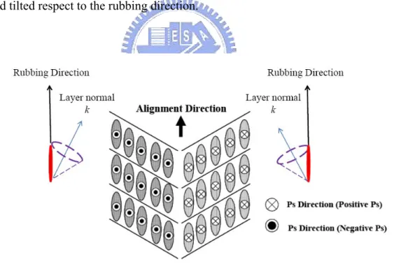
Dijion [26] studied alignment effect of different materials, defined and disclosed the sign of polarity as shown in Figure 4-1 and Table 4-1. The sign of the polarity was positive when the dipole on the surface was directed outward from the surface to the liquid crystal material and vice versa. PVA, Nylon 6, and HMDS were chosen.
34
Figure 4-1. Sign of surface polarity and the direction of the dipole moment.
Table 4-1. The sign of the polarity of different alignment layer.
Surface showing + polarity Surface showing – polarity
(CH3)3SiNHSi(CH3)3, HMDS CH3SiCl3
CH3NH(CH2)3Si(OCH3)3, MAP CH3(CH3O)3Si
Polyamide, PA6 or Nylon 6 (CH3)2ClSi(CH2)8SiCl(CH3)2
Polyvinylalchol, PVA Polyimide, PIX from Hitachi
In order to confirm of the polarity of the alignment layers, we adopted twisted FLC mode [27]. In this configuration, two crossed-rubbing cells were made. One was coated with positive polarity alignment materials we adopted and the other was coated with PI (Chisso, PIA-X201-G01). The FLC material used was R3206, with Ps~20
nC/cm2. As shown in Figure 4-2, if two alignment materials had different opposite
polarity, two specific layer directions should be observed in the cross-rubbing cell and layer normal of each cell was also different. Cells coated with PI, PVA, Nylon 6 were shown in Figure 4-3 and Figure 4-4. Because PVA and Nylon 6 had positive polarity while PI had negative polarity, the SmC* layers of the two former materials had opposite layer normal direction to that of PI.
35
HMDS was also tested. The layer structure was not appeared and demonstrated here because of its low boiling point, 125℃. R3206 had a high isotropic temperature and annealing process must be done or the layer structure will not appeared under POM’s observation. Changing another FLC material with a low isotropic temperature may solve this problem. R2301, a FLC material with spontaneous polarization around 9 nC/cm2 and low isotropic temperature of 88.6 ℃, was also tested. Unfortunately, layer
normal structure would only appear when the injected FLC material had high spontaneous polarization. Therefore, no layer structure was appeared even on nylon 6, PVA, and PI.
Figure 4-2. The relationship between layer direction and the polarity direction of the
alignment layers in twisted FLC mode when the sign of the spontaneous polarization was negative.
36
Figure 4-3. Pictures of the cross-rubbing cells taken by POM. Pictures at the right
were the magnified layer structures. (a) Layer structure in PI cell. (b)Layer structure in PVA cell.
Figure 4-4. Pictures of the cross-rubbing cells taken by POM. Pictures at the right
were the magnified layer structures. (a) Layer structure in PI cell. (b)Layer structure in Nylon 6 cell.
37
4.2 Hybrid cell
4.2.1 HMDS Hybrid Cell Test
Although HMDS did not show layer structure under twisted FLC configuration, it still worked in R2301, as shown in Figure 4-5. No horizontal defect appeared in the HMDS hybrid cell and the dark state was very good as shown in Figure 4-5 (a). However, the alignment was very bad in 50% R3206. We assumed HMDS was evaporated during the annealing process if 50% R3206 was injected into the cell. Figure 4-5 (c) was the hybrid cell only coating PI on one side. The texture was very similar to Figure 4-5 (b).
Figure 4-5. (a) HMDS hybrid cell injected with R2301. (b) HMDS hybrid cell
injected with 50% R3206. (c) Cell with only one side coated with PI and injected with 50% R3206.
38
In order to further to confirm if HMDS was evaporated because of its low boiling point, TN configuration for PI and HMDS was used. As shown in Figure 4-6, substrates coated with PI had great normally white state. HMDS cell baked at 90℃ had acceptable normally white state but that baked at 110℃ showed bad alignment. The results approved our assumption that HMDS was evaporated in 50% R3206 because we had to anneal FLC cells and 50% R3206 had high isotropic temperature over 110 ℃.
Figure 4-6. Normally white TN configuration of (a) PI alignment layer. (b) HMDS
alignment layer baked at 90℃ for 0.5 hour. (c) HMDS alignment layer baked at 110℃ for 0.5 hour.
39
4.2.2 Nylon 6 Hybrid Cell Test
Nylon 6 had verified to have opposite polarity with the PI we used here. Because Nylon 6 was a solid substance, meta-creosol [28] was used to solve it. Besides, unlike the general coating method, the alignment film uniformity would be bad if the solvent was dropped onto the substrate first and Nylon 6 was coating later. Figure 4-7 showed the results of 1 wt% Nylon 6 hybrid cells with single rubbing. Horizontal defect was not disappearing and distributing over the whole cell area in 50% R3206 and R2301. Because SSFLC alignment was a very difficult task even if the right material was found, several parameters, such as rubbing strength or baking time, had been modified but all fail. Finally, double rubbing method [29] was used.
Figure 4-7. 1 wt% Nylon 6 hybrid cells with single rubbing (a) 50% R3206 (b) R2301
Microscopic pictures of 50%R3206 injected into the Nylon 6 cells with double rubbing configuration were shown in Figure 4-8. Comparing with the cells coated with PVA or Nylon 6 on top and bottom substrates, the horizontal defect was successfully suppressed. The dark state was significantly improved as our expectations from elastic-continuum theory.
40
Figure 4-8. (a) The cell coated with Nylon 6 on both sides and injected with 50%
R3206. (b) (a) The cell coated with PVA on both sides and injected with 50% R3206. (c) and (d) are hybrid cells coated with Nylon 6 and PI.
As shown in Figure 4-8 (a) and (b), horizontal defect appeared if only Nylon 6 or PVA was coated onto the substrates. In hybrid cell A and B, better dark state without horizontal defect was achieved.
Also the results of R2301 with the same experiment setup were shown in Figure 4-9. Horizontal defect was also appeared in cells which were only coated with Nylon 6 or PVA and injected with R2301. In cell C and D, horizontal defect was suppressed so that better dark state was realized. Although some domains cell D still had extremely small horizontal defect, the effect of hybrid cell was obvious.
41
Figure 4-9. (a) The cell coated with Nylon 6 on both sides and injected with R2301.
(b) The cell coated with PVA on both sides and injected with R2301. (c) and (d) are hybrid cells coated with Nylon 6 and PI.
Besides, some very small silk-like white lines were appeared in 50% R3206 and R2301. The possible reason of the silk-like lines and small horizontal defect domain appearing of R2301 was that the substrates can not be located perfectly at the same place for the first and second rubbing. Slightly rubbing direction deviation may cause the molecules to align along two different directions which are almost parallel, resulting in the imperfection of Nylon 6 alignment.
42
Chapter 5
Conclusions
5.1 Summary
If the top and bottom alignment layers in SSFLC configuration were the same, FLC molecules, staying in uniform state mentioned in chapter 2, would have equal minimum free energy of two stable states so that horizontal defect appeared. We found that using two different alignment layers with opposite polarity made the free energy of one stable state be minimum so that LC molecules preferred to stay at that state. Consequently, horizontal defect no longer existed and light leakage problem from it could be improved greatly.
In the past, PVA and PI, which had opposite polarity, had been tested in our laboratory and the horizontal defect was successfully suppressed by the hybrid cell made from these two materials. Now two new materials, HMDS and Nylon 6, which had the same polarity as that of PVA were used to verify this again.
HMDS achieved mono-domain with R2301 but failed in R3206 because of low boiling point problem. Nylon 6 achieved horizontal defect-free state in R2301 and R3206. From the past research and our study, adopting hybrid cells with two different alignment materials having opposite polarity indeed solved horizontal defect. Only one state in the uniform state of SSFLC had the minimum energy if we adopted hybrid cell configuration.
43
5.2 Future Work
Polarity of alignment layer was related to the horizontal defect existence in SSFLC and PVA, HMDS, and Nylon 6 approved this. Testing more alignment materials with the same polarity is one of our targets. Besides, HMDS and Nylon 6 were not suitable materials for mass production application but PI and PVA were. To find out more alignment materials for mass production in SSFLC displays is the second target.
Equation 2-12 theoretically explained the reason and solution of horizontal defect. Now only the polarity sign of the materials can be known but the detailed mathematic numbers of the polarity value can not be measured precisely. How to measure the value is our target, too. Also if there is a critical value existing in the last part of equation 2-12 to make horizontal defect to disappear under the uniform state of SSFLC is also very interesting and deserved more study in the future.
44
References
1. P.J. Collings, “Liquid Crystals”, IOP Publishing Ltd,, 1990
2. J. P. F. Lagerwall and F. Giesselmann, Chem Phys Chem., 7, 20 (2006)
3. N.A. Clark and S.T. Lagerwall, Appl.Phys.Lett, 36, 899 (1980)
4. N. A. Clark and S. T. Langerwall, Jpn. J. Appl. Phys. Part 2, 27, 276 (1988)
5. T. P. Rieker, N. A. Clark, G. S. Smith, D. S. Parmar, E. B. Sirota, C. R. Safinya,
Phys. Rev. Lett., 59, 2658 (1987)
6. B.O. Myrvold, Liq. Cryst., 3 (9), 1255 (1989)
7. B.O. Myrvold, Liq. Cryst., 4 (6), 637 (1989)
8. B.O. Myrvold, Liq. Cryst., 7 (6), 261 (1990)
9. J. Kanbe, H. Inoue, A. Mizutome, Y. Hanyuu, K. Katagiri, S. Yoshihara,
Ferroelectrics, 114, 3 (1991)
10. M. Koden, T. Numao, N. Itoh, M. Shiomi, S. Miyoshi and T. Wada, Proc. Japan
Display’92, 519 (1992)
11. A. Tsuboyama, Y. Hanyuu, S. Yoshihara and J. Kanbe, Proc. Japan Display’92, 53 (1992)
12. M. Koden, H. Katsuse, N. Itoh, T. Kaneko, K. Tamai, H. Takeda, M. Kido, M. Matsuki, S. Miyoshi and T. Wada, Ferroelectrics, 149, 183 (1993)
13. M. Koden, T. Furukawa, M. Kabe, S. Okamoto, A. Sakaigawa, T. Sako, M. Sugino and A. Tagawa, J. C. Jones, M. H. Anderson, P.E. Dunn, J. R. Hughes, K.P. Lymer, V. Minter, K. G. Russell and A.J. Slanet, SID 98 Digest, 778 (1998)
14. H. Furue, Y. Iimura, H. Hasebe, H. Takatsu and S. Kobayashi, Proc. IDW’98, 209 (1998)
15. Y. Sato, T. Tanaks, H. Kobayashi, K. Aoki, H. Watanable, T. Takeshita, T. Ouchi, H. Takezoe and A. Fukuda, Jpn. J. Appl. Phys., 28, 483 (1989)
45
16. A. Mochizuki, K. Motoyoshi and M. Nakatsuka, Ferroelectrics, 122, 37 (1991) 17. T. Nonaka, J. Li, A. Ogawa, B. Hornung, W. Schmidt, R. Wingen and H.R. Duebal,
Liq. Cryst., 26, 1599 (1999)
18. T. Furukawa, M. Shigeta, H. Uchida and M. Koden, Proc. IDW’00, 251 (2000) 19. Y. Asao, T. Togano, M. Terada, T. Moriyama, S. Nakamura, J. Iba, Jpn. J. Appl.
Phys., 38, 5977 (1999)
20. T.C. Chieu, J.Appl. Phys. 64, 4680 (1988)
21. N. Manabe, M. Inoue, J. Akanowatari, AM-LCD’96/IDW’96, 237 (1996)
22. K. Myojin, H. Moritake, M. Ozaki, K. Yoshino, T. Tani, K. Fujisawa, Jpn. J. Appl.
Phys., 33, 5491 (1994)
23. J. S. Patel, J. W. Goodby, J. Appl. Phys., 59, 2355 (1986)
24. A. Hotta, R. Hasegawa, K. Takatoh, Jpn. J. Appl. Phys., 43, 6243 (2004)
25. F. Bruyneel, H.D. Smet, J. Vanfleteren, A. V. Calster, Opt. Eng., 40 (2), 259 (2001)
26. J. Dijon, Ferroelectric, 85, p.47 (1988)
27. K. Takatoh, H. Nagata and T. Saishu, Ferroelectrics, 179, 173 (1996) 28. D. Williams and L.E. Davis, J. Phys. D: Appl. Phys, 19, 37 (1986)
29. G. Padeletti, S. Pergolini, G. Montesperelli, A. D’Alessandro, F. Campoli, P. Maltese, Appl. Phys. A, 71, 571 (2000).