C.-L.Chen C.-J.Tseng
Indexing terms: Passive lossless snuhbers, Converters
Abstract: A general passive lossless snubber cell is proposed for use in DC/DC converters. The snubber is to suppress the turn-on loss of a MOSFET resulting from the reverse recovery current of the freewheeling diode. Energy recovery is achieved since the energy absorbed by the snubber during turn-on can be delivered to the output during turn-off. The simple structure and the absence of active components and resistors make this snubber a good alternative to a conventional RCD snubber or an active snubber. As an example, a boost converter equipped with the snubber is analysed. A IkW, IOOkHz prototype is implemented in the laboratory, and efficiency of 97% has been measured. Six basic non-isolated DC/DC converters equipped with the proposed snubber cell are also illustrated.
1 Introduction
Pulse width modulated (PWM) DC/DC converters have been widely used as switched mode power sup- plies in industry. The PWM technique is praised for its high power capability and ease of control. High power density and faster transient response of PWM DCIDC converters can be achieved by increasing the switching frequency. However, as the switching frequency increases, so do the switching losses and EM1 noises. High switching losses reduce the power capabilities of PWM DCiDC converters, and serious EM1 noises dis- turb control circuits.
Switching losses and EM1 noises are mainIy gener- ated during turn-on and turn-off switching transitions of PWM DC/DC converters. According to Pietkiewicz and Tollik [l], there are three different non-ideal com- mutation phenomena behind this problem. The domi- nant phenomenon is the turn-on transient caused by the reverse recovery current of the freewheeling diode.
During the turn-on process of a MOSFET in a boost circuit, the reverse recovery phenomenon makes the diode conducting reversely discharge itself. The drain current contains input current and the reverse recovery current increases instantaneously, and full output volt- age is applied between the drain and source because the
0 IEE, 1998
IEE Proceedings online no. 19981877 Paper received 23rd April 1997
The authors are with the Power Electronics Laboratory, Department of Electrical Engineering, National Taiwan University, Taipei, Taiwan
396
diode is still conducting. Multiplication of the drain current and drain-source voltage during the turn-on transient causes serious thermal problems. Fast dildt of the drain current also generates serious EM1 noises.
Several kinds of snubbers heve been presented to reduce switching losses. Active snubbers [2] need auxil- iary switches, and hence complex control strategies.
RCD snubbers [3] dissipate power through the resist- ances, and thus reduce efficiency. A passive lossless snubber can effectively restrict switching losses by using no active and no power dissipative components. The circuit structure is simplified, and circuit efficiency is also effectively improved.
In this paper, a passive lossless snubber for boost PFC is investigated in depth. Snubber circuit opera- tions are analysed, and component parameters can be mathematically determined. Experimental results from a 1 kW, IOOkHz boost PFC are used to verify the anal- ysis. The general snubber cell for the boost converter is
generalised to support the common non-isolated DC/ DC converters.
V
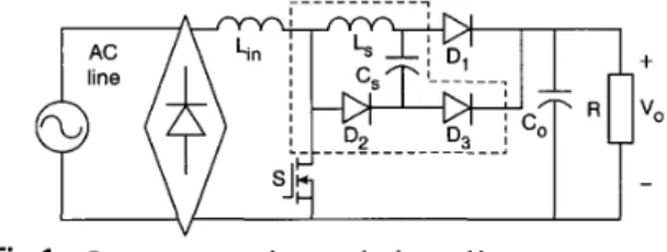
Fig. 1 Boost converter with passive lossless snubber
2 Boost PFC with a passive lossless snubber 2.1 Principle of operation
Fig. 1 shows a boost PFC with the studied snubber, which is encircled by dotted lines. During the turn-on process, diode D , conducts reversely to discharge itself. Growth rate of the reverse recovery current is restricted by the snubber inductor L,, which is placed in series with diode D1. After the reverse recovery of
D,,
it isturned off and the first resonance path is formed by L,, D2 and C,. The energy of L, in current form is trans- ferred to the snubber capacitor Cs in voltage form through diode D,. After switch S turns off and the first resonance is stopped, the reverse recovery energy is delivered back to the output through the second reso- nance path Vs-Lifl-L.r-Cs-D3- V,. This snubber absorbs the switching loss resulting from the reverse recovery current of diode D , and delivers it back to the output.
The circuit structure is simplified, and there are fewer components than with other energy recoverable snubbers.
2.2 Equivalent circuit analysis
T o analyse the steady-state operations in one switching cycle of the circuit shown in Fig. 1, the following assumptions are made:
(i) the output capacitor C, is large enough to assume that the output voltage Vu is constant and ripple-free. (ii) input voltage V, rectified from the AC voltage source is approximated to be constant in one switching cycle.
(iii) all semiconductor devices are assumed ideal, except the main diode D I .
(iv) the input inductor L,, is much greater than the snubber inductor L,.
to = S turns on t I = D , is turned off t2 =
Z,,
becomes zero and D, is turned offt3 = S turns off 0, and D3 are turned on t4 = D2 is turned off
t5 = Vc, becomes zero, D l is turned on and D , is turned off
Two cases are analysed according to different duty ratios:
Case
1 (long duty) : t0-tl-t2-t3-t4-ts-t0,Case 2 (short duty) : to-tl-t2
-t3-t&-t0,
In addition, the following six time steps are used:S turns off after I L ~ becomes zero.
S
turns off before I L ~ becomes zero. Based on these assumptions and classifications, the circuit operations of two cases in one switching cycle can be divided into six stages and are shown in Figs. 2-4, respectively. a b Fig. 2 N Stage 1 b Stage 2Equivalent circuits during one switching cycle
Stage 1 (Fig. 2a; to < t < t , )
Switch S turns on at to. The reverse recovery process makes diode D , conduct reversely to discharge itself. The inductor currents of
Li,
and L,, are given bywhere I d t o ) is the forward current through L,, and L , at to.
Stage
2
(Fig.2h;
Case 1: t l < t < t,, Case 2: t l < t < t,) The reverse recovery finishes and diode D 1 is off at t l . SinceD ,
is off, the reverse recovery current in L , cre- ates the first resonance path L,-D2-C, to charge C,, through D2. L , and C, create a one-way resonance because of diode D2. The current through L , and the voltage across C, are given byvc3(t)
=6 1 . .
sin(w(t -t l ) )
(3)(4)
ILLs(t) = I., cos(w(t -
h))
(6) 1
w=-
vmz
where
Z,.,.
is the peak value of the reverse recovery cur- rent through L, and D,. 0 < w(t - t , ) <nI2
since diodeD2 makes L,, and Cl, resonate in one direction.
Case 1 (long duty, t l < t < t,): L, and C, stop resonat- ing at t2 before switch S turns off at 1,. Time t2 is given by
(7)
At t2, I,, is equal to zero and Vc, is given by
Ir
Case 2 (short duty, t , < t < t,): the duty is too short so
that switch S turns off at t3 before the resonance stops at t2.
I
I I r r .
b
Equivulent circuits during one switchiug cycle for stuge 3 Fig. 3
( I Case I
h Case 2
Stage
3
(Fig.3a,
Case 1: t, < t < t,; Fig.3h,
Case 2: t 3Case 1 (long duty, t2 < t < t,): the current through L , is zero and the voltage across C, is constant after the first resonance is stopped by diode D2 at t2. The energy absorbed in L,, is completely delivered to C,. Before switch S turns off at t3, V,, is constant and I,, is zero, respectively.
< t < t 2 )
Case 2 (short duty, t3 < t < t2): diode D3 is turned on by the input inductor current Zdt3) when switch S turns off at t3. L,s and C, keep resonating through the path L,y-D2-C,s until the first resonance is stopped by diode D, at t Z . The input inductor current flows through diodes D2 and D3 to the output.
t
l
fVS
b C Fig. 4 u Stage 4 h Stage 5 c Stage 6Equivulent circuits during one switching cycle
Stage 4 (Fig. 4a; Case 1: t 3 < t < t4, Case 2 : t2 < t < t4)
Case 1 (duty cycle is long, t 3 < t < t4): diodes D2 and D3 are turned on by the input inductor current I d t 3 )
when switch S turns off at t3.
Case 2 (Duty cycle is short, t2 < t < t4): the first reso- nance is stopped and
Z
,
,
is equal to zero at t,. Time t2and the voltage V,, at t2 are also given by eqns. 7 and 8, respectively.
Cases 1 and 2: since diode D2 is on, the voltage across L,s is equal to Vc,y and makes ILs increase reversely to discharge C, to the output. When I,, increases to the input inductor current ZF(t4) at t4, diode D2 is turned off automatically. Assuming that the input inductor current is constant at this stage, time t4 when D, is automatically turned off and the voltage across C, at t4
are given by
where t, = t 3 in Case 1 and t,, = t2 in Case 2. Stage 5 (Fig. 4h; t4 < t < t,)
The second resonance is formed by Vs-Lj,-L,\-C,5-D3- Vu when diode D, is turned off at t4. In the second resonance, L,, L, and C, are discharging to the output. All of the reverse recovery energy is completely transferred back to the output when V,, is discharged
39x
to zero through diode D3 at t5. Assuming that the input inductor current is constant at this stage, time t5 when
V,, becomes zero is given by
Stage 6 (Fig. 4c; t5 < t < to)
The energy recovery of the snubber finishes when diode D , is turned on at t5. After that, the current ZF(t5) flows through diode D , instead of diode D3 to prevent C, from being charged reversely. Diode D , is turned on and D3 is turned off at t j . The input voltage source and the input inductor keep discharging to the output through diode D,. The circuit operation is the same as in Stage 1 when switch S turns on again at to in the next switching cycle.
I
i
:
I
I
I
\ to t l t 2 t3 t4 t5 to time Fig. 5ber for case 1 Key (lorig wnvefornis ~ I u y cycle long)
of the boost converter with pussivr losslrss snub-
ID2
I
ID3
to t i t3 t2 t4 t0
time
Fig. 6
ber for ruse 2 (short duty cycle) Key wuveforms of the boost converter with pussiw lossless snub- 3 General snubber cell for DC/DC converters
The general passive lossless snubber cell is designed to suppress the turn-on switching loss resulting from the reverse recovery process of the freewheeling diode. It IEE Pror.-Circuits, Devires Syst., Vol. 145. Nu. 6 . Deceinher 1998
follows that the proposed snubber can be generalised to support other basic DC/DC converters which suffer from the same switching
loss. A
general snubber cell isdefined and shown in Fig. 7. Nodes A and K are con- nected to the anode and the cathode of the converter freewheeling diode
D,,
respectively. Node A' is con- nected to the component that was connected to the anode of D1 in the original circuit.I I
IT-Fig. 7 Generd .snubber cell for D U D C convertet
J
a
b Fi .8
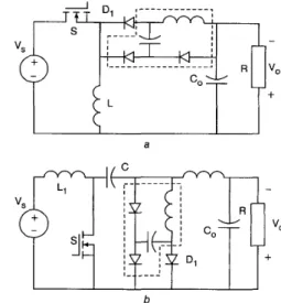
ii Buck converter with snubber h Boost converter with snubber
Bmic DC/DC converters ~ Y t l i the proposed snubher cells enihecl-
de7
The general snubber cell consists of one inductor L,s,
one capacitor C., and two diodes D2 and
D,.
The snub- ber inductor L,\ is placed in series with the freewheeling diode D , to restrict the growth rate of the reverse recovery current when the switch turns on. After the turn-on transient, L,, D2 and C, form a resonance path to transfer the absorbed energy from L, to C,. Energy stored in C,, is delivered to the output through D3 after the switch turns off. D3is
turned off and D , is turned on after Vcs is discharged to zero.Snubber operation principles discussed in the boost converter example can be extended to other topologies. Six basic DCIDC converters are shown in Figs. 8-10 with the proposed snubber cells embedded.
4 Experimental results
4.
I
Design exampleThe snubber inductor L, and snubber capacitor C,, are the two main elements to be designed. In Stage 4, diode D2 should be automatically turned off before the voltage of C, is discharged to zero, or the residual current through D2 will turn on D , and D3 for the whole switching period. In other words, I,, should be greater than IF according to eqn. 9. Snubber inductor L, should be as large as possible to decrease the reverse
recovery loss, but I,., should be kept larger than IF. L, can be determined by the following procedures.
a
b Fi .9
N Buck-Boost converter with snubber h Cuk convcrter with snubber
Basic D U D C converters with tlie proposed snubber c,ells cvnhcd de!
a
b
Fi . I O
( I Sepic convcrtcr with snubber
h Zeta converter with snubber
Basic DC/DC converters with the proposwt snubber cells etnhed- de7
Step 1: determine reverse recovery current peuk value I,., The drain current of the MOSFET will have a transi- tional peak value equal to I F
+
I,.,.. I,, can be deter- mined by setting the peak value of the drain current and then subtracting I FStep 2: culculute reverse current slope dIRldt I,.,. has the following relationship [4]:
I,., for specified I F and dIRidt can be found in a data book. The reverse current slope dIRldt can be obtained by using IF and I,, calculated in Step 1 in eqn. 12.
Step 3: determine snubber inductor L,\
The equation V = L,s(dItl,/dt) is used to determine L,, where V is the output voltage and I R is the current through D , as well as L,. L,? can be determined by
Ti
V d t
L - -
s - &
The voltage rating of
D ,
is equal to the output volt- age plus Vcs. The snubber capacitor C, should be as small as possible to reduce the resonant period and to prevent an excessively high voltage rating ofD,.
The recommended value of Vc, is 50-
lOOV and C, can be determined by eqn. 8.Table 1: Part list of the implemented prototype power circuit
Part TY Pe Part Value
s
IRFP460 L, 21rH D, HFAI 5TB60 c s IOOnF D* H FA 1 5TB60 L 180 KH D3 HFAl5TB60 C 940yF I I I I1
;
i
control circuitI.
I
using L4981A I - tFig. 11 Simplified circuit of implementedprorotype
145 150 160 170
time, ps
b
Fi .I2 Waveforms of snubber inductor current and snubber capacitor voiiage
a Experimental results h Simulation results
4.2 Experimental waveforms
To experimentally verify the principle of operation and the theoretical analysis, a prototype of 1 kW, lOOkHz boost converter with the passive lossless snubber is implemented. Control strategy is implemented with a L4981A. This prototype is regulated at 400V D C out- put with 220V AC input. A simplified circuit of the
400
implemented prototype is shown in Fig. 11, with the components specifications listed in Table 1.
The snubber inductor current and snubber capacitor voltage waveforms are shown in Fig. 12a, and PSPICE simulation results are shown in Fig. 12b. The wave-
forms in Fig. 12 can be collated with those of Vc, and
Z
,
,
in Fig. 6a.f
600_____
__ ________________________a
_______________ _____
__________
I ! -200______
--.---T-__________--
~,~_____________
______________
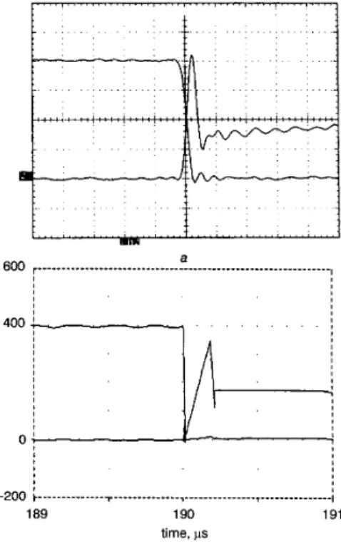
i 189 190 191 time, ps b Fig. 13 ber a Experimental results b Simulation resultsWaveforms of MOSFET commutation with the proposed snub-
The commutation waveforms of the MOSFET with the proposed snubber are shown in Fig. 13a, and
PSPICE simulation results are shown in Fig. 136.
Counterparts without the snubber are shown in Fig. 14a and b, respectively, to contrast with Fig. 13. It is easily seen that the turn-on loss is apparently reduced and the MOSFET commutates near the ZCS (zero-current-switch). The reason for the ZCS is the discharge of the parasitic drain-source capacitance of
the MOSFET during the turn-on process. This
switching loss can only be removed by resonant converter techniques or active snubbers. It can also be seen that the growth rate of the drain current is effectively eliminated. EM1 noises are reduced due to the slower dildt of drain current. Efficiency of 97% at 1kW loading has been measured by the Voltech PM3000A.
5 Conclusion
A general passive lossless snubber cell for DC/DC converters has been proposed. The general snubber cell is composed of only one inductor, one capacitor and
two diodes. The cell is designed to suppress turn-on switching losses caused by the reverse recovery current
of
the freewheeling diode. Steady-state circuit operations of a boost circuit with the proposed snubber have been analysed. Experimental waveforms of the MOSFET commutation show that the snubber can effectively suppress the reverse recovery loss and eliminate the dildt of the drain current. The snubber inductor and capacitor for the boost topology can be precisely determined by the presented design. The circuit operation analysis and design rules are also valid when applying the snubber to other topologies.References
PIETKIEWICZ, A., and TOLLIK, D.: ‘Snubber circuit and Mosfet paralleling considerations for high power boost-based power-factor correctors’. INTELEC ’95, pp. 4 1 4 5
LIN, R.L., and LEE, F.C.: ‘Novel zero-current-switching-zero-
voltage-switching converters’. PESC ’96, pp. 438442
FINNEY, S.J., WILLIAMS, B.W., and GREEN, T.C.: ‘The RCD snubber revisited’. IAS ’93, pp. 1267-1273
MOHAN, N., UNDELAND, T., and ROBBINS, W.: ‘Power electronics: converters, applications and design’ (Wiley, 1989), pp. 462467