Study of quantum confinement effects on hole mobility in silicon and germanium
double gate metal-oxide-semiconductor field-effect transistors
Chun-Jung Tang, Tahui Wang, and Chih-Sheng Chang
Citation: Applied Physics Letters 95, 142103 (2009); doi: 10.1063/1.3244205 View online: http://dx.doi.org/10.1063/1.3244205
View Table of Contents: http://scitation.aip.org/content/aip/journal/apl/95/14?ver=pdfcov
Published by the AIP Publishing
Articles you may be interested in
Dramatic enhancement of low electric-field hole mobility in metal source/drain Ge p-channel metal-oxide-semiconductor field-effect transistors by introduction of Al and Hf into SiO2/GeO2 gate stack
Appl. Phys. Lett. 103, 122106 (2013); 10.1063/1.4821546
Channel direction, effective field, and temperature dependencies of hole mobility in (110)-oriented Ge-on-insulator p-channel metal-oxide-semiconductor field-effect transistors fabricated by Ge condensation technique
J. Appl. Phys. 109, 033709 (2011); 10.1063/1.3537919
Physics of strain effects in semiconductors and metal-oxide-semiconductor field-effect transistors
J. Appl. Phys. 101, 104503 (2007); 10.1063/1.2730561
Valence band structure of ultrathin silicon and germanium channels in metal-oxide-semiconductor field-effect transistors
J. Appl. Phys. 98, 024504 (2005); 10.1063/1.1948528
Hole confinement and mobility in heterostructure Si/Ge/Si p -channel metal–oxide–semiconductor field effect transistors
J. Appl. Phys. 81, 8079 (1997); 10.1063/1.365415
This article is copyrighted as indicated in the article. Reuse of AIP content is subject to the terms at: http://scitation.aip.org/termsconditions. Downloaded to IP: 140.113.38.11 On: Wed, 30 Apr 2014 14:49:57
Study of quantum confinement effects on hole mobility in silicon
and germanium double gate metal-oxide-semiconductor
field-effect transistors
Chun-Jung Tang,1Tahui Wang,1,a兲and Chih-Sheng Chang2
1Department of Electronics Engineering, National Chiao-Tung University, Hsinchu 30050, Taiwan 2Taiwan Semiconductor Manufacturing Company, Hsinchu 30077, Taiwan
共Received 22 July 2009; accepted 15 September 2009; published online 5 October 2009兲
Quantum confinement effects on hole mobility in silicon and germanium double gate p-channel metal-oxide-semiconductor field-effect transistors共MOSFETs兲 are studied by using a Monte Carlo method. Uniaxial stress and channel/substrate orientation effects are considered. Our result shows that the hole mobility in a共100兲/关110兴 silicon well decreases with a decreasing well thickness, which is in agreement with the experimental result. The hole mobility in a germanium channel MOSFET, however, exhibits a peak in a sub-20 nm well because of the interplay between intrasubband and intersubband scatterings. © 2009 American Institute of Physics.关doi:10.1063/1.3244205兴
Double-gate 共DG兲 metal-oxide-semiconductor field-effect transistors 共MOSFETs兲 and fin field-effect transistor have been considered as promising alternatives to bulk MOSFETs in 22 nm technology node and beyond1–3 due to their immunity to short channel effects. Recently, advanced channel materials with higher carrier mobility than bulk Si, such as Ge共Ref.4兲 and III-V materials,5have attracted much attention. Experimental works have shown the possibility that the inversion carrier mobility can be further improved in quantum structure MOSFETs by a subband modulation.6,7 However, there has been little work on Ge-channel DG-pMOSFETs addressing valence subband and substrate/ channel orientation effects on hole mobility.
In this paper, we analyze quantum confinement effects on hole mobility as a function of a body thickness in Si- and Ge-channel DG-pMOSFETs. The low-field hole mobility is calculated by a Monte Carlo method.8 The impact of sub-strate orientation on hole mobility is also evaluated. Further-more, the effect of uniaxial compressive stress is discussed. Instead of the effective-mass approximation, the valence subband structures for two-dimensional holes in Si- and Ge-channel DG-pMOSFETs are calculated self-consistently from the coupled Poisson and Schrödinger equations with a six-band Luttinger–Kohn Hamiltonian including spin-orbit coupling.9 The Bir–Pikus deformation potentials10 are also included to take into account the stress effect. In addition, an appropriate rotation matrix is employed when dealing with substrate orientations other than the共100兲 direction.11,12 Ma-terial parameters, including Luttinger parameters, deforma-tion potentials, and elastic constants used in the simuladeforma-tion, are given in Refs. 13–15. Relevant scattering mechanisms, including acoustic phonon scattering, optical phonon scatter-ing, and surface roughness scatterscatter-ing, are considered in the Monte Carlo simulation.16–19The scattering parameters of Si and Ge are calibrated from a conventional Si MOSFET and from a SiGe-on-insulator device, respectively.18
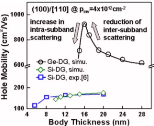
Figure1 compares the hole mobility as a function of a body thickness in 共100兲/关110兴 Si- and Ge-channel DG-pMOSFETs, where 共兲 and 关兴 are the notations of substrate
orientation and channel direction, respectively. The choice of the关110兴 channel in Si is because it has a larger stress effect. The inversion hole density, pinv, is set to be 4⫻1012 cm−2. The simulated hole mobility in a Si-channel decreases mono-tonically with a body thickness, which is consistent with the experimental data.6Unlike a Si channel, the hole mobility in a Ge channel shows a turn-around characteristic with a body thickness. When a body thickness reduces, the hole mobility increases gradually to a maximum around TGe= 16 nm, and then decreases drastically. In the window of inversion hole density and body thickness considered in this work, where the transverse effective electric field is about 0.12 MV/cm in a Ge channel, the surface roughness scattering has a minor effect on the hole mobility in a Ge channel. The same con-clusion can be found in Ref. 20. Therefore, surface rough-ness scattering should not affect the existence of a mobility peak in a Ge channel. Moreover, the calculated hole mobility at TGe= 28 nm is about 617 cm2/V s, which deviates from the bulk value of Ge. This is due to larger phonon deforma-tion potentials in a MOSFET than in a bulk material, result-ing from stress at gate dielectric and semiconductor interface.21
The turn-around behavior of the mobility in a Ge-channel can be explained in the two following aspects: over-lap integral and energy separation between subbands. As a
a兲Electronic mail: [email protected].
FIG. 1. 共Color online兲 Simulated hole mobility as a function of a body thickness in共100兲/关110兴 Si- and Ge-channel DG-pMOSFETs. The experi-mental result for Si channels is plotted for comparison.
APPLIED PHYSICS LETTERS 95, 142103共2009兲
0003-6951/2009/95共14兲/142103/3/$25.00 95, 142103-1 © 2009 American Institute of Physics
This article is copyrighted as indicated in the article. Reuse of AIP content is subject to the terms at: http://scitation.aip.org/termsconditions. Downloaded to IP: 140.113.38.11 On: Wed, 30 Apr 2014 14:49:57
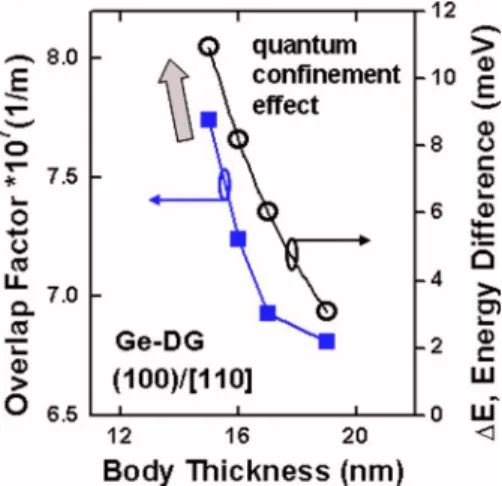
body thickness decreases, the energy difference, ⌬E, be-tween the first subband 共heavy hole band兲 and the second subband共heavy hole band兲 increases owing to quantum con-finement effects, as shown in Fig.2. Because of less chance to be scattered to the second subband, inversion holes have a larger mobility owing to a smaller intersubband scattering rate. On the other side, the intrasubband scattering rate in-creases due to an increase of an overlap integral. The con-finement effect on the overlap integral can be understood from the illustration in Fig.3. When a smaller body thickness is considered, the wave function has a wider distribution in momentum space due to the uncertainty principle. For a fixed phonon momentum in the quantized direction qz, only
the shaded region in Fig. 3 contributes to the overlap inte-gral. A broader distribution in momentum space results in a larger overlap factor 共Fig.2兲 and thus a larger intrasubband
scattering rate. The interplay between intersubband and in-trasubband scatterings opens a window of a body thickness where the scattering rates can be minimized, giving rise to a peak in hole mobility, as shown in Fig.1. Unlike a Ge chan-nel, the lowest two subbands in a共100兲/关110兴 Si channel are heavy-hole and light-hole bands, respectively, due to the high degree of degeneracy of heavy and light holes in Si.7 For a decreasing well thickness, the larger energy separation re-duces hole population in the light-hole subband and leads to a decrease of hole mobility.
Moreover, the substrate orientation effect in Ge channels is evaluated in Fig. 4. The same scattering parameters of
surface roughness scattering for 共100兲 and 共110兲 substrates are assumed. Three points are worth noting. First, quantum confinement induced mobility enhancement is again ob-served in共110兲 substrate. Second, the 共110兲 substrate shows an anisotropy of energy dispersion, such that the共110兲/关1¯10兴 channel direction exhibits a highest mobility, and then the 共110兲/关001¯兴 共result not shown in Fig.4兲. The higher mobility
in 共110兲/关1¯10兴 than in 共100兲/关110兴 is attributed to a lower conductivity effective mass. Third, the peak mobility in 共110兲/关1¯10兴 occurs at a smaller body thickness. This reason is that a smaller energy difference between the lowest two subbands is obtained in Ge 共110兲 substrate.
Finally, the effect of 0.3 GPa uniaxial compressive stress on normalized hole mobility is shown in Fig.5. Note that the channel direction is also the uniaxial stress direction. Gener-ally, the uniaxial compressive stress removes the heavy hole and light hole degeneracy and alters the warping of the va-lence bands. Thus, the effective mass becomes anisotropic with applied stress. The constant energy contours of the first subband for 共100兲 and 共110兲 substrates are depicted in the figure. In Fig.5, at a large body thickness, the stress induced hole mobility enhancement in 共100兲/关110兴 and 共110兲/关1¯10兴 channel directions is comparable due to the same bulk pi-ezoresistance coefficients.22 For a smaller body thickness, the quantum confinement effect plays a role and the energy difference from the uniaxial compressive stress and surface
FIG. 2. 共Color online兲 The body thickness dependence of an overlap factor and an energy difference between the lowest two subbands in共100兲/关110兴 Ge-channel DG-pMOSFETs.
FIG. 3. Illustration of the body thickness dependence of valence subband energy and overlap factor. The shaded region corresponds to an overlap integral. A narrower quantum well has a larger energy separation between subbands and a larger overlap factor.
FIG. 4. 共Color online兲 Comparisons of the hole mobility and subband en-ergy difference in共100兲/关110兴 and 共110兲/关1¯10兴 Ge-channels.
FIG. 5.共Color online兲 Ge hole mobility as a function of a body thickness in 共100兲/关110兴 and 共110兲/关1¯10兴 channel directions with and without an uniaxial compressive stress of 0.3 GPa. The mobility is normalized to the one with-out stress effect. The constant energy contours in共100兲 and 共110兲 substrates are also plotted.
142103-2 Tang, Wang, and Chang Appl. Phys. Lett. 95, 142103共2009兲
This article is copyrighted as indicated in the article. Reuse of AIP content is subject to the terms at: http://scitation.aip.org/termsconditions. Downloaded to IP: 140.113.38.11 On: Wed, 30 Apr 2014 14:49:57
field is additive, which is responsible for the slight shift of the peak mobility.
In conclusion, the effects of channel/substrate orientation and uniaxial compressive stress on hole mobility versus body thickness in Ge-channel DG-pMOSFETs are investigated. The peak mobility in both共100兲/关110兴 and 共110兲/关1¯10兴 chan-nel directions can be achieved at a certain body thickness due to the interplay between intersubband and intrasubband scat-terings. Furthermore, the hole mobility can be further im-proved when the uniaxial compressive stress is applied to 共100兲/关110兴 or 共110兲/关1¯10兴 channel direction.
The authors共C.J.T., T.W., and C.S.C.兲 would like to ac-knowledge financial support from National Science Council, Taiwan, under Contract No. NSC-96-2628-E-009-165-MY3 and from Taiwan Semiconductor Manufacturing Co.
1F. Balestra, S. Cristoloveanu, M. Benachir, J. Brini, and T. Elewa,IEEE
Electron Device Lett. 8, 410共1987兲.
2H. Kawasaki, M. Khater, M. Guillorn, N. Fuller, J. Chang, S. Kanakasa-bapathy, L. Chang, R. Muralidhar, K. Babich, Q. Yang, J. Ott, D. Klaus, E. Kratschmer, E. Sikorski, R. Miller, R. Viswanathan, Y. Zhang, J. Silver-man, Q. Ouyang, A. Yagishita, M. Takayanagi, W. Haensch, and K. Ishi-maru, Tech. Dig. - Int. Electron Devices Meet. 2008, 237.
3T. Mérelle, G. Curatola, A. Nackaerts, N. Collaert, M. J. H. van Dal, G. Doornbos, T. S. Doorn, P. Christie, G. Vellianitis, B. Duriez, R. Duffy, B. J. Pawlak, F. C. Voogt, R. Rooyackers, L. Witters, M. Jurczak, and R. J. P. Lander, Tech. Dig. - Int. Electron Devices Meet. 2008, 241.
4R. Xie, T. H. Phung, W. He, Z. Sun, M. Yu, Z. Cheng, and C. Zhu, Tech. Dig. - Int. Electron Devices Meet. 2008, 393.
5N. Goel, D. Heh, S. Koveshnikov, I. Ok, S. Oktyabrsky, V. Tokranov, R.
Kambhampati, M. Yakimov, Y. Sun, P. Pianetta, C. K. Gaspe, M. B. San-tos, J. Lee, S. Datta, P. Majhi, and W. Tsai, Tech. Dig. - Int. Electron Devices Meet. 2008, 363.
6S. Kobayashi, M. Saitoh, and K. Uchida, Tech. Dig. - Int. Electron De-vices Meet. 2007, 707.
7G. Tsutsui, M. Saitoh, and T. Hiramoto, Dig. Tech. Pap. - Symp. VLSI Technol. 2005, 76.
8C. Jacoboni and L. Reggiani,Rev. Mod. Phys. 55, 645共1983兲. 9J. M. Luttinger and W. Kohn,Phys. Rev. 97, 869共1955兲.
10G. L. Bir and G. E. Pikus, Symmetry and Strain-Induced Effects in
Semi-conductors共Wiley, New York, 1974兲.
11A. T. Pham, C. Jungemann, and B. Meinerzhagen,Solid-State Electron. 52, 1437共2008兲.
12S. Rodríguez, J. A. López-Villanueva, I. Melchor, and J. E. Carceller,J.
Appl. Phys. 86, 438共1999兲.
13T. Low, M. F. Li, Y. C. Yeo, W. J. Fan, S. T. Ng, and D. L. Kwong,J.
Appl. Phys. 98, 024504共2005兲.
14J. D. Wiley,Solid State Commun. 8, 1865共1970兲.
15M. V. Fischetti and S. E. Laux,J. Appl. Phys. 80, 2234共1996兲. 16M. V. Fischetti, Z. Ren, P. M. Solomon, M. Yang, and K. Rim,J. Appl.
Phys. 94, 1079共2003兲.
17M. De Michielis, D. Esseni, Y. L. Tsang, P. Palestri, L. Selmi, A. G. O’Neill, and S. Chattopadhyay,IEEE Trans. Electron Devices 54, 2164 共2007兲.
18A.-T. Pham, C. Jungemann, and B. Meinerzhagen,IEEE Trans. Electron
Devices 54, 2174共2007兲.
19S. E. Thompson, G. Sun, Y. S. Choi, and T. Nishida,IEEE Trans. Electron
Devices 53, 1010共2006兲.
20L. Donetti, F. Gamiz, F. G. Ruiz, N. Rodriguez, and A. Godoy Proceeding of the Meeting Abstracts of the Journal of the Electrochemical Society, 2009共unpublished兲, Vol. 901, p. 959.
21M. Lundstrom, Fundamentals of Carrier Transport, 2nd ed.共Cambridge University Press, Cambridge, 2000兲.
22C. S. Smith,Phys. Rev. 94, 42共1954兲.
142103-3 Tang, Wang, and Chang Appl. Phys. Lett. 95, 142103共2009兲
This article is copyrighted as indicated in the article. Reuse of AIP content is subject to the terms at: http://scitation.aip.org/termsconditions. Downloaded to IP: 140.113.38.11 On: Wed, 30 Apr 2014 14:49:57